ELECTROCHEMICALLY SWITHABLE
PLASMONIC SURFACES
A THESIS
SUBMITTED TO THE MATERIALS SCIENCE AND
NANOTECHNOLOGY PROGRAM
OF THE GRADUATE SCHOOL OF ENGINEERING AND SCIENCE
OF BILKENT UNIVERSITY
IN PARTIAL FULLFILMENT OF THE REQUIREMENTS
FOR THE DEGREE OF
MASTER OF SCIENCE
By
Nihat Serkan KARAYALÇIN
January , 2014
i
I certify that I have read this thesis and that in my opinion it is fully adequate, in scope and in quality, as a thesis for the degree of Master of Science.
___________________________________ Asst. Prof. Dr. Aykutlu Dana (supervisor)
I certify that I have read this thesis and that in my opinion it is fully adequate, in scope and in quality, as a thesis for the degree of Master of Science.
__________________________________ Assoc. Prof. Dr. Cengiz Koçum
I certify that I have read this thesis and that in my opinion it is fully adequate, in scope and in quality, as a thesis for the degree of Master of Science.
___________________________________ Assist. Prof. Dr. Bülend Ortaç
Approved for the Graduate School of Engineering and Science:
___________________________________ Prof. Dr. Levent Onural
ii
ABSTRACT
ELECTROCHEMICALLY
SWITHABLE PLASMONIC
SURFACES
Nihat Serkan KARAYALÇIN
M.S. in Materials Science and Nanotechnology
Supervisor: Assist. Prof. Dr. Aykutlu Dana
January 2014
In this study, we design and produce grating coupled surface plasmon surfaces which are switched by electrochemistry. Grating structures are fabricated using digital versatile discs (DVDs) which are commercially available. According to atomic force microscopy (AFM) results, we categorize the different grating structures in two groups, namely shallow and deep gratings. Plasmonic properties of the surfaces are investigated using numerical simulations. Gold and silver are used as plasmon supporting metallic layers on gratings. Refractive index sensitivity of the plasmon resonances are studied using deionized water, air and glycerol solutions as the dielectric media and results are compared with simulations. Experimental results are coherent with the simulations in terms of reflection spectra.
Electrochemical switching of plasmonic properties may have applications in tunable and switchable filters, as well as enhanced colorimetric sensing. We deposit ultrathin films of copper on plasmonic surfaces and investigate reversible changes in the plasmonic properties. Copper sulfate is selected as the electrolyte. Cyclic voltammetry is performed on plasmonic surfaces while monitoring optical reflectance. Copper is observed to deposit in the form of nanoislands on silver and gold films rather than uniform thin films. The effect of copper deposition on the plasmonic properties of the grating structure is simulated by Lumerical software and
iii
is seen to be two fold. For small effective thickness of copper nanoislands, the plasmon resonance condition shifts, whereas for thicker copper deposition plasmonic resonances are eliminated.
Finally, copper's oxidation and reduction reactions are controlled by changing applied voltage thus shifting the resonance wavelength. Resonances are switched reversibly multiple times not only for different molarities but also for different grating sructures and plasmon supporting metallic layers . In summary, we demonstrate that plasmonic properties of nanostructured metallic surfaces can be controlled by electrochemistry. Switchable resonance surfaces can be used as dynamic filters or may enhanced contrast in plasmon resonance imaging applications.
Keywords: Plasmonics, Grating Coupled Surface Plasmon Resonance,
iv
ÖZET
ELEKTROKİMYASAL OLARAK
DEĞİŞTİRİLEBİLEN
PLAZMONİK YÜZEYLER
Nihat Serkan KARAYALÇIN
Yüksek Lisans, Malzeme Bilimi ve Nanoteknoloji Bölümü Tez Yöneticisi: Yrd. Doç. Dr. Aykutlu Dana
Ocak 2014
Bu çalışmada , elektrokimyasal olarak değiştirilebilen kırınım ağı kuplajlı yüzey plazmon yüzeylerinin tasarımı ve üretimini gerçekleştirdik. kırınım ağı yapılarını , ticari olarak temin edilebilen çok amaçlı sayısal diskler(DVDs) kullanılarak ürettik. Atomik kuvvet mikroskobu sonuçlarına göre, kırınım ağı yapılarını sığ ve derin olarak 2 kategoriye ayırdık. Numerik simülasyonlar kullanılarak yüzeylerin plazmonik özellikleri inceledik. Altın ve gümüşü, kırınım ağı yapıları üzerinde plazmon destekleyici metalik katman olarak kullandık. Plazmon rezonanslarının kırılma indisi hassasiyetini , deiyonize su ,hava ve gliserol solüsyonunu dielektrik ortam olarak kullanarak araştırdık. Deneysel sonuçların yansıma spektumu cinsinden numerik simülasyonlarla uyumlu olduğunu gözlemledik.
Plazmonik özelliklerin elektrokimyasal olarak değiştirilebilirliği, ayarlanabilir ve değiştirilebilir filtreler ayrıca artırılmış kolorimetrik algılama uygulamalarında kullanılabilir. Plazmonik yüzeylerin üzerine çok ince bakır tabaka indirgedik ve plazmonik özelliklerde geri çevrilebilir değişiklikleri araştırdık. Elektrolit olarak bakır sülfat seçtik. Plazmonik yüzeylere periyodik voltmetri uygularken optik yansımayı takip ettik. Bakırın, altın ve gümüş filmlere düzgün ince tabakalar yerine nanoadalar şeklinde indirgendiğini gözledik. Bakır indirgenmesinin kırınım ağı yapılarının plazmonik özellikleri üzerindeki etkileri Lumerical yazılımını kullanarak
v
simüle ettik ve etkinin 2 katı olduğunu gözledik. Bakır nanoadaların küçük efektif kalınlığı için plazmon rezonans durumunun kaydığı , kalın bakır indirgenmesinde plazmonik rezonansın yok olduğunu gözlemledik.
Sonunda, bakır yükseltgenme ve indirgenme reaksiyonlarını uygulanan voltaj değiştirilerek kontrol ettik ve bu sayede rezonans noktasını kaydırdık. Rezonansları sadece değişik molarite için değil ayrıca değişik kırınım ağı yapıları ve değişik plazmon destekleyici metalik katmanlar içinde birçok kez geri çevrilebilir şekilde değiştirdik. Özetlemek gerekirse , nanoyapılı metalik yüzeylerin plazmonik özelliklerinin elektrokimya yardımıyla kontrol edilebileceğini kanıtladık. Değiştirilebilir rezonans yüzeyler, dinamik filtreler yada plazmon rezonans görüntülemede kontrast artırma uygulamalarında kullanılabilir.
Anahtar Kelimeler: Plazmonik , Kırınım Ağı Kuplajlı Yüzey Plazmon Rezonans,
vi
Acknowledgement
I would like to thanks to my supervisor Dr. Aykutlu Dana for his valuable guidance.
I would also like to thank my group members; Sencer Ayaş, Öner Ekiz, Hasan Güner, Burak Türker and Mustafa Ürel.
I owe thanks to my parents and friends for their support and patience.
vii
viii
Table of Contest
1.Introduction
1
2.Theoretical Background
5
2.1 Surface Plasmon ... 5
2.1.2 Excitation Methods of Surface Plasmons ... 9
2.1.2.1 Prism Coupling ... 10
2.1.2.2 Grating Coupling ... 11
2.2 Electrochemistry ... 12
3.
Characterization of Grating Structures
153.1 Surface Topography of Grating Structures... 15
3.2 Numerical Simulations ... 18
4.Production
24 4.1 Plasmonic Gratings ... 24 4.2 Electrochemical Cell ... 26 4.3 Experimental Setup ... 29 4.4 Electrolites... 29
5.
SPR and Electrochemical Experiments,
Lumerical Simulations
305.1. SPR Experiments ... 30
5.2 Cyclic Voltagram ... 36
5.3 Lumerical Simulations ... 39
6.
Electrochemically Switchable Plasmonic
Surfaces
42ix
6.1 Shallow Grating Experiments... 42
6.2 Deep Grating Experiments ... 45
7.
SPR Colorimetric Sensing and Imaging
48
7.1 SPR Colorimetric Imaging ... 48
7.2 SPR Colorimetric Sensing ... 50
x
List of Figures
Figure 2.1 : Surface plasmons between metal ,dielectric media ... 5 Figure 2.2 : Geometry for wave propagation at metal-dielectric interface ... 6 Figure 2.3 : Dispersion relations between wavevector of light in air and wavevector of plasmon ... 9 Figure 2.4: Prism coupling geometry : (a) Kretschmann configuration , (b) Otto configuration ... 10 Figure 2.5: The plasmonic dispersion relation for grating coupling ... 12 Figure 2.6: Electrochemical reaction process ... 13 Figure 3.1: AFM image of Verbatim Blueray Disc ; (a) 3d surface topography, (b) Period and depth ... 16 Figure 3.2: AFM image of Maxell Pro-x DVD ; (a) 3d surface topography, (b) Period and depth ... 17 Figure 3.3: AFM image of Maxell R+DVD; (a) 3d surface topography, (b) Period and depth ... 17 Figure 3.4: (a)Numeric aperture of experimental setup , (b) Diffraction Angle v.s Wavelength of Reflected Orders ... 18 Figure 3.5: Wavelength interrogation simulation of blueray grating structure when
DI water as dielectric media and Al, Au, Ag as plasmon supporting metallic layer ... 19 Figure 3.6: Wavelength interrogation simulation of Shallow grating structure when DI water as dielectric media and Al,Au,g as plasmon supporting metallic layer ... 20 Figure 3.7: Wavelength interrogation simulation of Deep grating structure when DI water as dielectric media and Al, Au, Ag as plasmon supporting metallic layer ... 20 Figure 3.8: Wavelength interrogation simulation for different thicknesses of copper
layer on Ag deposited surface when DI water as dielectric media ... 21 Figure 3.9: Wavelength interrogation simulation for different thicknesses of copper
xi
Figure 3.10: Angle interrogation simulation of Deep grating structure with different incident ligth angle; DI water as dielectric media and Au as plasmon
supporting metalic layer ... 22
Figure 4.1 :Sample preparation steps : (a)splitting it into 2 parts, (b) nitric acid threatment ... 24
Figure 4.2: (a) AFM image of gratings after metal deposition (b) Sem image of coated sample ... 25
Figure 4.3: Xps image of sample : survey analysis ... 26
Figure 4.4: First version of electrochemical cell ... 27
Figure 4.5: Final version of channel ... 28
Figure 4.6: Optical experimental setup ... 29
Figure 5.1: Reflection spectrum of Shallow grating structure when 60 nm Ag on 10 nm germanium as metallic layer, DI water as dielectric media ... 31
Figure 5.2: Reflection spectrum of Shallow grating structures when 60 nm Ag on 10 nm Ge as metallic layer, air as dielectric media ... 31
Figure 5.3: Reflection spectrum of Shallow grating structures when 60 nm Au on 10 nm Ge as metallic layer, air as dielectric media ... 32
Figure 5.4: Reflection spectrum of Shallow grating structure(other side of DVD's) when 60 nm silver over 10 nm germanium as metallic layer, air as dielectric media ... 32
Figure 5.5: Reflection spectrum of Shallow grating structure(other side of DVD's) when 60 nm Ag over 10 nm Ge as metallic layer, DI water as dielectric media. ... 33
Figure 5.6: Reflection spectrum of Deep grating structure when %100 DI water(n=1.33) as dielectric media ... 34
Figure 5.7: Reflection spectrum of Deep grating structure when %36 glycerol solution (n =1.3787) as dielectric media ... 34
Figure 5.8: Reflection spectrum of Deep grating structure when %53 glycerol solution (n=1.4025) as dielectric media ... 35
Figure 5.9: Reflection spectrum of Deep grating structure when %100 glycerol (n=1.47399) as dielectric media ... 35
Figure 5.10: Cyclic voltagram of 0,05 M CuSO4 solution between ±0,4 V... 36
xii
Figure 5.12: Sem image of silver coated grating surface with 0.05M CuSO4 solution after applying -0,4 volt during ; (a)3 seconds , (b)7 seconds, (c)10 seconds, (d)15 seconds ... 38 Figure 5.13: Grating structure simulated by Lumerical software ... 39 Figure 5.14: Simulation for 90 nm width periodically empty area with 10,40,60 nm heights copper nanoislands... 40 Figure 5.15: Simulation for 80 nm width periodically empty area with 10,40,60 nm heights copper nanoislands... 40 Figure 6.1: ±0,4 V applied voltage; silver as plasmon supporting metallic layer and 0,01 M CuSO4 solution as dielectric media ... 43 Figure 6.2: ±0,4 V applied voltage; silver as plasmon supporting metallic layer and 0,05 M CuSO4 solution as dielectric media ... 43 Figure 6.3: ±0,4 V applied voltage; silver as plasmon supporting metallic layer and 0,1 M CuSO4 solution as dielectric media ... 44 Figure 6.4: ±0,4 V applied voltage; silver as plasmon supporting metallic layer and 0,02 M CuSO4 solution as dielectric media ... 45 Figure 6.5: ±0,4 V applied voltage; silver as plasmon supporting metallic layer and 0,05 M CuSO4 solution as dielectric media ... 45 Figure 6.6: ±2V applied voltage; gold as plasmon supporting metallic layer and 0,05 M CuSO4 solution as dielectric media ... 46 Figure 6.7: Sem image of silver coated grating structure after switched several times
... 47 Figure 7.1: Rectangular structures on Deep grating based golden surface ... 49 Figure 7.2: Surface image of Deep grating based golden surface with 0,02M CuSO4 ... 49 Figure 7.3: Images of surfaces according to applied voltage and period ... 51 Figure 8.1: (a) top view, (b) bottom view of potantiostat circuit ... 53
1
CHAPTER 1
Introduction
The excitation of surface plasmons is first observed from unusual reflected pattern when polarized light is sent on metallic surface. Later, scientists started to use surface plasmons for practical applications such as characterization of thin films. Gas sensing application is the first attempt to use Surface Plasmon Resonance (SPR) as sensor [1]. After that, the number of studies based on SPR biosensor application continiously increased. In the later 1980s, SPR is used first time for imaging by Rothenhausler and Knoll [2]. Because SPR provides label-free and real time measurments, interest in SPR studies increased over the last decades. SPR is one of the most widely used method for implementing label free biosensors[3-10]
Connection between electric and chemistry is set by discovery of Alessandro Volta in 1973 .Volta produced the primitive battery by putting different metal at opposite side of moistened paper. In 1800, Nicholson and Carlisle seperated water into hydrogen and oxigen by applying voltage (electrolysis). After that, Faraday indicated the relation between applied current and amount of electrolysis production. Even though electrochemistry is discovered in 1800s , its applications accelerated after 1950s. Like SPR , electrochemistry is used in sensor applications [11-19]
There is a large number of publications on using electrochemistry and plasmon resonances for biosensor applications. Li et al. use SPR and electrochemical measurements together to investigate interaction between α-actinin and negatively charged lipids membrane. They demonstrate that α-actinin can bind to negatively charged lipids membrane by change in SPR and cyclic voltagram results. They use the both techniques to increase the reliability [20]. Toda et al. use SPR to produce
2
electrocemical enzyme immunoassay. They immobilize antibody on gold electrode by monitoring the SPR signal [21].
Some researchers realize the high potential of combining electrochemistry and SPR. Panta et al. observe the deposition and stripping steps of mercury due to cyclic voltagram by SPR [22]. Also Huang et al. detect intermediate reaction product by SPR. They control hydroquinone–benzoquinone (HQ–BQ) reaction by cyclic voltagram and semiquinone radical anion (BQ) is detected as intermediate reaction product[23]. On the other hand Vasjari et al. use SPR to observe the redox reactions of mercury. They use cyclic voltagram to control oxidation and reduction reactions of mercury and measure the changes in SPR angle.[24]
Plasmonic imaging by electrochemistry studies also find place in more prestigious journals. Tsuboi et al. use electrochemical deposition of silver nano particles on Indium Tin Oxide (ITO) to make multicolor devices by using localized plasmon resonance (LSPR) properties of silver nanoparticles. They are able to tune the plasmonic properties across the visible spectrum in this way.[25] Shan et al. enhance contrast in plasmonic imaging to determine electrochemical current due to redox reactions of Ru(NH3)3+ on gold electrode.[26]
Especially inspired from Shan et al. study, possibility of monitoring thin layers by electrochemically control of surface's plasmonic properties with grating coupled mechanism is our main motivation. For these purpose, we design and produce plasmonic surfaces based on gratings which fullfits all the requirements of the excitation of plasmons with in a compact and economical setup. We realize dynamic filters and plasmonic imaging with these structures. Accoding to results presented in this thesis, we may assert that deep grating based plasmonic surfaces have great potential in colorimetric biosensor applications.
We organized the thesis as follows ;
In chapter 2, we explain the surface plasmon, and the dispersion relation of surface plasmons by deriving the equations. We mention the most commonly used methods for excitation of surface plasmons; grating and prism coupling. We explain the Kretschmann and Otto configuration for prism coupling method in detail. We give the details of the grating coupling mechanism while indicating benefits. Finally we explain why we use grating coupling method in this study.
3 In chapter 3, we characterize the commercially available Digital versatile discs (DVDs). DVDs are used as the plasmonic platform because of their commercially availability and presence of perfect fabricated structures. We determine the surface topography of DVDs by Atomic Force Microscopy(AFM). According to AFM results, we categorize the gratings in two groups proportional to their depths; namely Deep and Shallow. We investigate the plasmonic properties of the gratings against different plasmon supporting layers and dielectric medias by numerical simulations. We identify that surface plasmon resonance based on Shallow grating is usually sharp , while Deep grating based plasmon resonance is usually broad. Besides we simulate copper nanolayer on the surfaces for both gratings and observe shifts in resonance upon electrochemical modification thus we demonstrate that swithable plasmonic surfaces can be realized by electrochemical control of redox reactions. Finally we simulate angle dependance of the gratings and determine that smooth results can be achived with 0o incident light angle.
In chapter 4, we give details of obtaining the plasmonic gratings from commercial DVDs. First we obtain the burried grating structure by splitting the DVDs and clean before metal deposition by nitric acid and ultrasonic cleaner. Then we deposit gold and silver as plasmon supporting layer and germanium as adhesive layer by thermal evaporator to produce plasmonic surfaces. We design and produce electrochemical cell multiple times to eliminate bubble and conduction problem. We describe the optical experimental setup for 0o incident angle measurements. We explain the configuration of the optical experimental setup in detail .
In chapter 5 , we perform SPR experiments to observe coherence between the samples and numerical simulation results for both grating structures. According to experimental results, we determine the samples are produced appropriately. At the same time , we calculate sensitivities of the systems and compare them with literature. We perform cyclic voltagram experiments to investigate electrochemical properties of copper sulfate solutions. We determine redox currents for solutions with different concentrations thus we observe that ± 0.4 volt guarantees the oxidation and reduction for all solutions. Based on this result, we decide to perform constant voltage experiments rather than cyclic voltagram. We apply constant
4
voltage with different period to different samples to investigate copper deposition formation on surface by Scanning Elecron Microscopy(SEM). According to the SEM images, we determine that copper deposites on surface as nanoislands rather than thin layers. We simulate effect of copper nanoislands on plasmonic properties of the surfaces by Lumerical software. We determine that for different thicknesses and densities of copper nanoislands, plasmon resonance shifts.By this way, we demonstrate theoretically that plasmonic properties of the surfaces can be controlled by electrochemistry
In chapter 6, we start electrochemical SPR experiments. According to the experiments, we show that plasmonic properties of surfaces can be controlled by electrochemistry. We perform experiments not only for different grating structures but also for different plasmon supporting metallic layers. As a result of the experiments, we notice that origin of resonance shifts in course of time after switching multiple times when silver as plasmon supporting metallic layer. We repeat the experiments for gold as metallic layer with higher applied voltage and observe no such problems for these conditions. We take image of surface by SEM after the experiments and determine the source of the problem that copper existence on surface after oxidation process.
In chapter 7, we use Deep grating based plasmonic surfaces's broad resonance profile for plasmonic imaging.For this purpose, we produce rectangular structures on surfaces by optical litography and etching process. We image these structures on golden surfaces by simple camera. On the other hand, we perform the electrochemical experiments and provide color changes of surface reversibly. By this way , we demonstrate that the Deep grating based plasmonic surfaces can be used for colorimetric biosensor applications.
In last chapter , we conclude the study and explain the future works in detail. In order to control electrochemical reactions precisely, we decide to change the system with 2 electrodes to 3 electrodes is called potentiostat circuit. We explain the potentiostat circuit which is produced in detail. Finally, we mention about the future plan that designing a smart phone attachment to demonstrate plasmonic imaging can be performed by smart phones,
5
CHAPTER 2
Theoretical Background
In this chapter, we explain the theoretical background of surface plasmons, it's excitation methods, electrochemistry and ion-potential distribution in electrochemical cell in detail.
2.1 Surface Plasmon
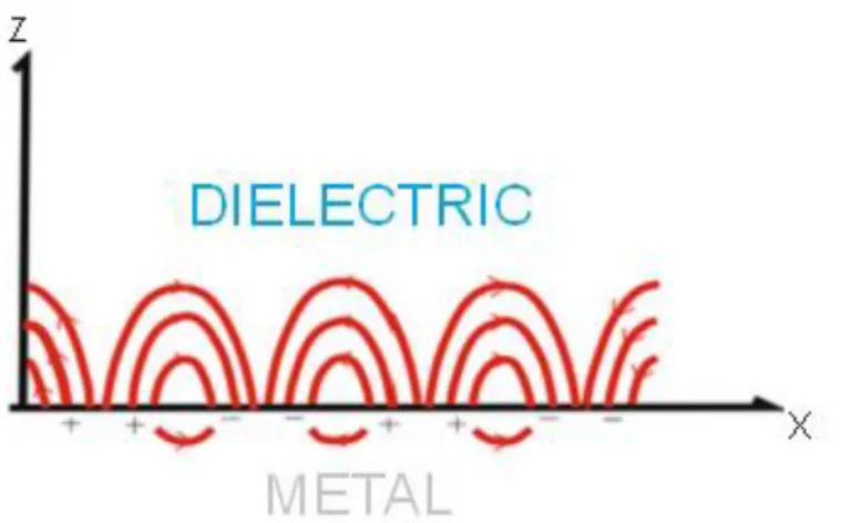
Surface plasmons are free electrons which are oscillating paralel between the metal-dielectric interfaces. They generate electromagnetic fields thus they are called as electro-magnetic waves.
2.1.1 Surface Plasmons at Metal Dielectric Boundaries
6
Changes in surface charge density provide electromagnetic field. Amount of the field depends on distance from the surface. It decreases exponentially in both media. Surface plasmons mode is explained by Maxwell’s equations. Assume that nonmagnetic media and ε does not change dramatically with distance,
(2.1) Due to the harmonic time dependence, we can write
and put this into equation 2.1 and we obtain,
(2.2)
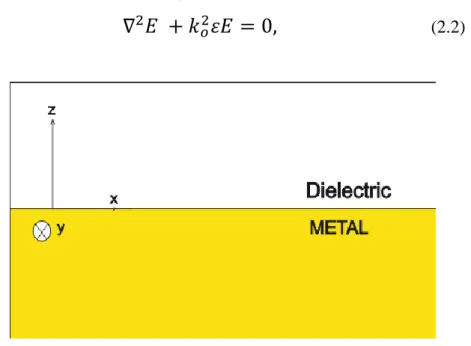
Figure 2.2: Geometry for wave propagation at a metal-dielectric interface
Considering such a propagation geometry as shown in Figure 2.2, ε is depending on only z-direction, wave propagates in x-direction and no variation in y axis
, wave equation of surface plasmon is
, where β is
propagation constant of surface plasmon in x direction. Then we put new wave equation into equation 2.2 and we get,
, (2.3)
This equation satisfy E field but we have H field as well. We need to make connection between these 2 components thus we use Maxwell’s Curl Equations,
7
(2.5)
Propagation is along x-axis(
) and as mentioned
,
, (2.6)
(2.7)
(2.8)
, (2.9)
(2.10)
(2.11) We can solve these equations for p polarized (transverse magnetic) and s polarized (transverse electric) modes. Ex, Ez and Hy components are exist for TM mode whereas Hx, Hz and Ey are exist for TE mode. Then wave equation for Tm mode ,
,
(2.12)(2.13)
(2.14)
Similarly for Te mode ,
(2.15) , (2.16)
=0
, (2.17)As mentioned , evanescent decay occurs in z-axis. If we have Tm polarized wave propagating on the surface , for z>0 ,
, (2.18)
8
, (2.20) Similarly for z<0,
, (2.21)
, (2.22)
, (2.23)
Continuity should be provided (z=0) for , by deriving equations 2.18 , 2.19 , 2.21 and 2.22 ,
,
(2.24)
(2.25) From equation 2.25 , are positive so one of the electrical permitivities
is negative. This lead us that surface plasmons are exist while one media is insulator another is conductor. must satisfied equation 2.21 , for z>0 and z<0 ,
, (2.26)
, (2.27)
Now we can introduce dispersion relation of surface plasmons, by inserting equation 2.25 into equation 2.26, and equation 2.27 ,
, (2.28)
We find dispersion relation of surface plasmon for Tm polarization now we drive the equations for Te polarization for the same geometry and z>0 ,
(2.29)
(2.30)
, (2.31) Similarly for z<0,
(2.32)
9
(2.33)
(2.34)
Continuity have to be provided for , thus
, continuity also be provided for , so
, are positive , must be equal to 0. It demonstrates that only Tm polarizated light can excite surface plasmons.
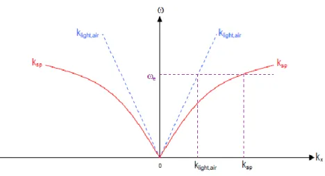
Figure 2.3: Dispersion relations between wavevector of light in air and wavevector of plasmon
In Figure 2.3 , no intersection between dispersion curves therefore direct excitation of surface plasmons is impossible.
2.1.2 Excitation Methods of Surface Plasmons
Excitation occurs when wave vectors of incoming light and surface plasmons are paralel. Incoming light transfers it's energy to the surface plasmons when excitation conditions meet. Dark bands are seemed at reflected light due to absorpted energy of incoming light. These bands are observed in terms of angle or wavelength of reflected light. These bands are also very sensitive to the surrounding of metallic media. Little changes in refractive index cause detectable movement at reflection spectra which has high potential for biosensor applications . As explained, direct
10
excitation is impossible, so different techniques must be used to excite surface plasmons. The most common methods are ; prism and grating coupling systems. 2.1.2.1 Prism Coupling
The most common method to excitation of surface plasmons is "Attenuated Total Reflection(ATR)" based prism coupling. The relation between dispersion equations of surface plasmon and light is;
,(2.35)
From equation 2.35 , momentum matching is not possible unless using high index prism since the prism increases . There are two types of prism coupling configuration; Kretschmann [27] and Otto geometry [28].
Figure 2.4 : Prism coupling geometry : (a) Kretschmann configuration , (b) Otto configuration
At Kretschman geometry, prism contacts directly with metal , while dielectric media contacts with prism at Otto geometry. Otto configuration is preferred where prism and metal conduction is unwanted. But the main problem of Otto configuration is addiction to the dielectric thickness of the system which is disrupted easily. Kretschmann geometry is more common due to easy implementation and sensitivity. Light come into the prism and reflected from prism-metal interface but evenascently penetrates into metal. Excitation is performed by evenascent wave at metal-dielectric interface. During excitation, energy transfer takes place between
11
light and surface plasmon and changes in reflection spectrum in terms of wavelength or angle can be monitored.
2.1.2.2 Grating Coupling
Grating is explained as regular repetitation of periodic pattern. Periodic structure provides different diffracted orders. Incident light is diffracted into multiple orders with different diffraction angles. Excitation occurs when momentum of diffracted orders along the interface is equal to the momentum of surface plasmons. Assume that we have incident light with wavevector ko and incident angle θ, horizantal
wavevectors kd of diffracted orders are;
,
(2.36) m represents the diffraction order which is integer, ᴧ is period of grating. From the equation 2.36 , wavevector of incident light can be improved with grating by changing incident angle of light and period of grating. As mentioned, momentums are must be equal so we can write equations for coupling condition as ,
, (2.37)
, (2.38)
Surface profile of grating has translational symmetry, so the plasmonic dispersion has also symmetry; therefore surface plasmons are excited both forward and backward directions . " ± " sign represents change in direction in equation 2.38. Therefore 2 splitted resonance dips shown at reflectance spectrum except 0o angle of incident light. When 0o angle of incident light, two resonances are overlapping and they seem as one. This condition is both advantage and disadvantage for several applications. For example, in biosensor applications, shift in resonance can be monitored from two dips and it provides double check in experimental results. But in filter applications, second unwanted filter may demolish experiments.
12
Figure 2.5: The plasmonic dispersion relation for grating coupling
Kretschmann configuration needs prism , costly equipments and large area and also studies about grating coupled method are low thus in this study we prefer grating coupling method to excite surface plasmons.
2.2 Electrochemistry
Electrochemistry is a branch of chemistry which is based on chemical reaction between electronic(metal v.s) and ionic conductor(electrolite). We call electrochemical reaction as if chemical reaction occurs by applying external voltage or voltage is produced by a chemical reaction.
In electrochemical reaction, electron transfer occurs between electrodes and electrolite. If the reaction ends with electron gain, it is called reduction and oxidaton is vice versa. Standart electrode potential of electrodes must be higher than ions in solution otherwise spontaneous reactions occurs.
Although gold, silver and aluminum are popular for plasmonic applications, aluminum is not appropriate for chemical applications due to it's chemically reactive properties.
13
Figure 2.6 : Electrochemical reaction process
In ionic solutions, surface charges are equalized by counter ions in solution to preserve electrical neutrality. Several counter ions reduce on the surface and the others distribute in solution within the electrical double layer .
Assume that we have surface which is 1d planar and has constant potential , determined by number of ions on surface. The potential will decay with distance (x) and will be zero far away from surface. We can call the potential as a funtion of x; .
We can generaly describe the potential with poisson equation;
,
(2.39)ρ
is charge density ,is electrical permittivity
.
This equation is for three dimensions (3D) but our system is one dimesion(1d) therefore;
=
,
(2.40)is constant and boundary condition of the equation is ;
,
(2.41),
(2.42)Now we want to relate potential with the concentration of the ions in solution. We can explain that the ions in solution obey Boltzman distribution. Boltzman equation is ;
14
(2.43) Where , number of ions per unit volume at , concentration of ions in solution , is charge of an electron , is the valence of the ion , is boltzmann constant and T is temperature. From equation 2.43 we can define charge density ;
, (2.43) Now we have function relates charge density to potential distribution of the ions. If we have multiple ions in solution ;
,
(2.44)Now we have relation about charge density so we substituted back up into poisson equation and called Poisson-Boltzmann equation;
,
(2.45) No general solution to this equation unless some assumption. First assumption is surface potential is typically low ,<< . So we can linearize the equation;
,
(2.46) if we call ,,
(2.47) K is kappa,then the equation is simply ,(2.48) This equation has a simple solution if we apply boundary condition;
or
,
(2.49) According to the equations, we explain potential and ion distribution in electrochemical cell.15
CHAPTER 3
Characterization of Grating Structures
In this chapter , we analyz digital versalite discs(DVDs) to obtain grating structures by Atomic Force Microscopy(AFM). Then we simulate the grating structures by PC GRATE sofware to examine their plasmonic properties for different simulation parameters such as plasmon supporting layer , dielectric media and grating structure.
3.1 Characterization of grating structures
We explain the reason of usage of grating coupling method in previous chapter. Now it's time to supply grating structures.Commercially available DVDs has perfect fabricated and cheap grating structures so we decide to use DVD as grating mold.
We observe surface topograhies of DVDs by AFM . AFM has 2 modes ; contact and tapping. In contact mode, AFM tips contact with surface and discover topographies of it with high resolution but tip or sample can be damaged at any moment. In tapping mode , we can discover surfaces without contact but of course with low resolution. By this way we reduce the possibility of damage in tip and sample . Our structures are not too small therefore we decide to use tapping mode.
We start AFM studies with Blueray discs becasue no information about these structures in literature thus this study will help researchers to uncover plasmonic properties of Blueray discs.
16
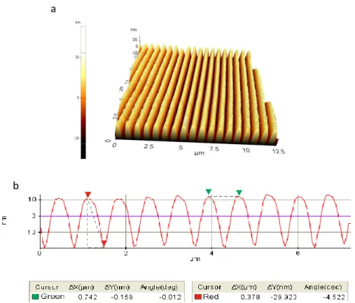
Figure 3.1:AFM image of Verbatim Blueray Disc ; (a) 3d surface topography, (b) Period and depth
According to AFM studies , we determine 15 nm depth and 305 nm period for blueray structure ,besides it seems like sinus trapezoidal(figure 3.1). The grating structures are smaller thus non-contact mode of AFM can not expose surface topography appropriately. Whereupon the period is repeated but the depth is not. Moreover blueray discs can not be easily availible in markets thus usage of blueray disc will problem to researchers who would use it in study. Also blueray discs are very costly, DVDs can be used as grating mold in applications but blueray discs can not under these conditions.
a
17
Figure 3.2:AFM image of Maxell Pro-x DVD ; (a) 3d surface topography, (b) Period and depth
Figure 3.3:AFM image of Maxell R+DVD; (a) 3d surface topography, (b) Period and depth
a
b
a
18
According to the studies based on DVD grating structures, periods are common as 740 nm but depths are different thus we chategorize gratings in 2 groups ; namely Deep ve Shallow(Figure 3.2 and 3.3).
We investigate plasmonic properties of the gratings by numerical simulations. By this way , we observe the effect of incident light angle , different dielectric medias and plasmon supporting layers on the plasmonic properties of grating surfaces.
3.2 Numerical Simulations
In order to investigate plasmonic properties of the surfaces, we perform numerical simulations. We use PCGrate Version 6.5 software which provides different simulation parameters such as wavelength and angle of incident light. The grating structures are derived from AFM experiments.
Figure 3.4: ( a)Numeric aperture of experimental setup , (b) Diffraction Angle v.s
Wavelength of Reflected Orders
The numeric aperture of the experiemental setup is 25o. Simulations are performed on 0. reflected order since the other orders reflect with angles higher than numerical aperture of the experimental setup (Figure 3.4). We select gold(Au), Silver(Ag) and Aluminum(Al) as plasmon supporting metallic layer in simulations due to their plasmonic properties. Deionized water(DI water) is selected as dielectric media.
The most important parameter is defining grating structures appropriately while simulation. The structures are not defined properly and they will show differences in
19
experiments therefore we repeat AFM experiments multiple times to provide reliability As we observe, blueray discs grating structures are sinus trapezoidal. Edge profile of structures are defined by frequency of sinus function. Sinus frequency is determined as 2 hz because the edge profile of structures are not so sharp.
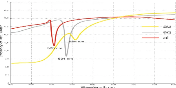
Figure 3.5: Wavelength interrogation simulation of blueray grating structure when DI water as dielectric media and Al, Au, Ag as plasmon supporting metallic layer
While DI water (n=1.33) as dielectric media, Al and Ag have sharp resonance profile thus we claim that these metallic layers are usable in plasmonic filter and biosensor applications.(Figure 3.5). But this is not valid for Au coated surfaces. While using blueray grating based plasmonic surfaces with 0o incident light angle and DI water combination, useful results are impossible.
The second part of the simulations are performed on Shallow and Deep grating structures.
20
Figure 3.6: Wavelength interrogation simulation of Shallow grating structure when DI water as dielectric media and Al,Au,Ag as plasmon supporting metallic layer
Figure 3.7: Wavelength interrogation simulation of Deep grating structure when DI water as dielectric media and Al, Au, Ag as plasmon supporting metallic layer
We study plasmonic properties of Deep and Shallow grating structures for different plasmon supporting layers. Shallow grating based plasmonic surfaces has sharp plasmon resonance, but when Au as metallic layer , no significant resonance profile is observed (Figure 3.7)
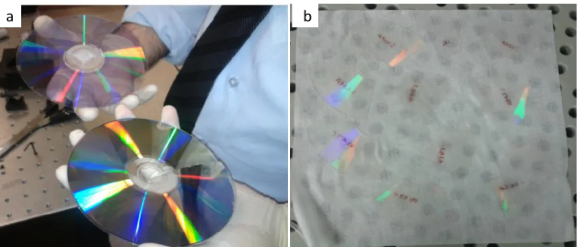
Plasmonic properties of Deep grating based surfaces open a completely different application area to us. Thanks to it's broad resonance profile , it behaves like band pass filter. Changes in refractive index can be detected in terms of color changing.
21
By this way, we can detect biomolecular interactions without costly equipments such as spectrometer.It can be used not only for sensing but also for imaging applications. Thin layer blocks the electrochemical interaction with surfaces, hence contrast differences occurs between coated and uncoated parts. By this way, structures on surfaces can be monitored by camera. In Shan et al.'s study , they use prism coupling mechanism with ccd camera but according to the simulations, we can assert that this can be performed with grating coupled method and basic camera.
Up to now, we investigate plasmonic properties of DVDs by numerical simulations. After this time, we simulate to observe effect of copper nanolayer on plasmonic properties of plasmonic surfaces. We prefer copper for deposited material because we use copper sulfate solutions in experiments. We will explain why copper sulfate is selected as electrolite in further chapters.
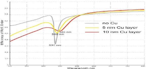
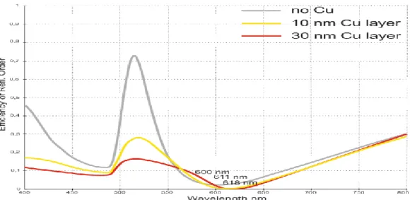
Figure 3.8: Wavelength interrogation simulation for different thicknesses of copper layer on Ag deposited surface when DI water as dielectric media
20 nm copper nanolayer shifts plasmon resonance almost 15 nm . On the other hand the thicker layer oblitirate plasmon resonance (Figure 3.8)
22
Figure 3.9: Wavelength interrogation simulation for different thicknesses of copper layer on Ag deposited surface when DI water as dielectric media
We observe the thin layer of copper shifted plasmon resonance for the both grating structures and thicker layer oblitirates it. By this way we theoretically demonstrate that plasmonic properties of surfaces can be controlled by electrochemically .Up to this time, simulations are performed with 0o incident light angle but we need to investigate angle dependence of system. For this reason, we simulate the surfaces to observe effect of different angle
Figure 3.10: Angle interrogation simulation of Deep grating structure with different incident ligth angle; DI water as dielectric media and Au as plasmon supporting
23
According to the angle interrogation simulations , our structures are highly dependent on incident light angle so we have to build optical experimental setup on 0o incident light angle .
In summary, we investigate surface topographies of DVDs and blueray discs by AFM. We simulate grating structures for different plasmon supporting layer by PC Grate software. According to the simulation results, we observe that different grating structures have different plamonic properties. Especially Deep grating structures have great potential in SPR colorimetric sensing and imaging applications . After that we investigate effect of copper thin layers on plasmonic properties of surfaces. By this way, we demonstrate that plasmonic properties of surfaces can be controlled by electrochemistry. Finally we search the angle dependance of structures by numerical simulations. We determine that only experiments with 0o angle of incident light can realized our expectations.
24
Chapter 4
Production
In this chapter, we explain the production of plasmonic gratings and electrochemical cell, preparation of electrolites and building of experimental setup in detail.
4.1 Plasmonic Gratings
Figure 4.1: Sample preparation steps : (a) splitting it into 2 parts, (b) nitric acid threatment
We start with isolation of grating structures from DVDs. First, sample is cut with sciccors then splitted into 2 parts by hand. Nitric acid treatment is applied during 2 seconds to remove contaminations on sample (Figure 4.1) . Nitric acid treatment period is critical ; above 2 seconds , nitric acid damages the surface. After that 10 minutes ultrasonic cleaning is applied. We squeeze nitrogen on surface to dry. No need acetone treatment and also isopropanol should not be used. These steps must be carried on at clean room enviroment since the splitted parts are polluted easily which effects results dramatically.
25 For the requirement of plasmonic surfaces, we deposite metals on surfaces by thermal evaporator. Silver layer is damaged after electrochemical reactions, therefore we use germanium as adhesive layer. Although adhesive layer provides development, further improvements are needed. Higher coating thickness is better but sources of thermal evaporator should be used economically. According to our experiences, 60 nm metal thickness is sufficient to prevent transmittance of light and production of plasmonic surfaces. We keep coating rates below 0.5 angstrom / second for uniform coating.
Figure 4.3: (a) AFM image of gratings after metal deposition (b) Sem image of coated sample
The grating structure of samples is protected in terms of period and depth (Figure 4.3). It demonstrated that the simulations are valid for the coated samples. Current regulation in thermal evaporator is also important. Fast changes in applied current causes sudden fracture on thermal evaporator boat. Rotation speed of sample must be optimized for uniform coating. Materials have high melting point such as
b a
26
germanium are also problem. Boat can resist high temperature and current must be selected appropriately according to the coated materials.
The gratings produced are analyzed in terms of structure and purity by AFM and X-ray photoelectron spectroscopy (XPS). XPS is spectroscopic technique that indicates existance of elements within a material. X-ray stimulates surface and XPS simultaniously measures kinetic energy and number of scattered electron in range 10 nm to surface. Range is small and number of scattered electron is important therefore high vacuum condition is mandatory [29].
Ag3d
Figure 4.4 : Xps image of sample : survey analysis
Survey search reveals the existance of Ag on surface as well as no contamination(Figure 4.4). Now we sure that silver deposition is realized properly.
4.2 Electrochemical Cell
We start to create electrodes. First, we use shadow mask to split electrodes. But we can not adjust size of shadow mask appropriately thus big amount of sample is lost. For this reason, we deposite metal on DVD and split electrodes by tweezer. But the electrodes should be splitted properly by tweezer and conduction test must be performed by multimeter.
27
Conduction with electrodes is the most problematic part of the system. We start with silver pen which is liquid phase of silver but not good option due to following reasons;
Poisinous ;gas mask have to be wear while using,
Have to wait at least 30 minutes to dry
Need conductive base
Second option is neomidyum magnet which provides good probing forwhy;
Easy implementation
Low resistance between probes and electrodes
Figure 4.6: First version of electrochemical cell
After conduction problem is solved, we start to product electrochemical cell. We cut 2 same size glass epoxy parts and open 2 screw holes to each other to provide pressure by screw. We put elastic ring between part and sample to determine height and width of the channel. Then we open 2 small holes and placed small pipes for tubing (Figure 4.6). Unfortunately we can not solve the bubble problem. Therefore we design new channel according to the problems. Samples bent after cutting and scraptining procedure thus we use glass wider than sample as basement and double-sided band as fixing material. On the other hand neonidyum magnets are used in
28
both conduction and fixing material on tables which are magnetized such as optical tables. The following steps are performed during production of electrochemical cell;
1. We cut appropriately sized piece from coated sample
2. We scrapt small area at middle of the sample to create electrodes by tweezer
and check with multimeter that no conduction
3. We take wider glass than sample and use double-sided band to fix sample on the
glass properly.
4. We cut appropriately sized piece from double-sided band and open a hole at
middle of it by punch to fix channel onto the sample. The double-sided band also blocks solution which protrudes from channel
5. We place magnet at the edges of electrodes
6. We put small glass piece onto the channel to flatten bending
Figure 4.7: Final version of channel
By production of new electrochemical cell, we solve both the conduction and bubble problems. We create easily and quickly electrochemical cells by optimization of production process.
29
4.3 Experimental Setup
Figure 4.8: Optical experimental setup
We can not use ellipsometer because light is sent and collected with 0o. Thanks to building of optical experimental setup by ourselves, we have mobile and easily adaptable system. We provide broad band light with gaussion distrubution from Zeiss light source . We carry light to the fiber colimator by fiber optic cable. Fiber colimator parallelizes light and we adjusted polarizer to change polarization of parallelized light. Beam splitter lets us sending and collecting light at the same time. We use lens to focus light to the fiber optic cable. The fiber optic cable carry light to the spectrometer (Figure 4.8) .Thanks to carrying light with fiber optic cable, light source and spectrometer can be changed easily. By this way, we can work in full range of light. After a while, we change the spectrometer with camera for imaging applications in further experiments.
4.4 Electrolites
We mention that plasmonic properties can be controled by electrochemistry. For this purpose, we prepare copper sulfate(CuSO4) solution as electrolite due to copper's reduction potential which is lower than silver and gold. Solid copper sulfate is supplied from Merck Industry. Solutions with different concentrations are prepared by AND GR200 precision weighning balance. According to the reduction potential of eletrode, different solutions can be prepared to perform different experiments. But copper sulfate is easily available and coherent with Au and Ag so we prefer it as electrolite. We prepare copper sulfate solutions with different molarities to observe effect of different concentrations on plasmonic properties.
30
CHAPTER 5
SPR and Electrochemical
Experiments, Lumerical Simulations
In this chapter , we perform SPR experiments to investigate plasmonic properties of surface for different grating structures and plasmon supporting metallic layers. Cyclic voltagram experiments are performed to investigate redox reactions of copper. Finally we use Lumerical software to simulate copper nanoislands with different heights and densities on plasmonic surfaces.
5.1. SPR Experiments
After production process , we perform SPR experiments to observe coherence between simulations and samples. By this way , we determine the differences and it's reasons. We perform experiments not only for DI water but also for air as dielectric media. Experiments are performed with 0o incident light angle as explained in previous chapter. But we don't carry out with different angles of incident light , it may be performed in future to observe angle dependence of the systems. We explain in chapter 4 that we split DVDs into 2 parts but the simulations are performed for one. But here, we perform the experiments for the other side and investigate the important parameters of surface plasmon resonance by comparing results.
31
Figure 5.1 : Reflection spectrum of Shallow grating structure when 60 nm silver on 10 nm germanium as metallic layer, DI water as dielectric media
Figure 5.2 : Reflection spectrum of Shallow grating structures when 60 nm Ag over 10 nm Ge as metallic layer, air as dielectric media
As you can notice from experiments based on silver surfaces, the results are coherent with the numerical simulations(Figure 5.2). By this way , we check both accuracy of simulations and production process. Sensitivity is calculated as 0.00660 refractive index unit(RIU) which is coherent with literature[30].
32
Figure 5.3 : Reflection spectrum of Shallow grating structure when 60 nm gold as metallic layer, air as dielectric media
We do not observe significant resonance profile for golden surace while DI water as dielectric media which is coherent with simulations. The coherence between simulations and experiments for the golden surface proves that structures can be applied in various metals. But as we mention, 0o incident light angle with Shallow grating and DI water combination is not suitable. Maybe experiments with different angles can provide usable combinations.
Figure 5.4 : Reflection spectrum of Shallow grating structure(other side of DVD's) when 60 nm silver over 10 nm germanium as metallic layer, air as dielectric media
33
Figure 5.5 : Reflection spectrum of Shallow grating structure(other side of DVD's) when 60 nm Ag over 10 nm Ge as metallic layer, DI water as dielectric media.
As you can notice, simulations and experiments are coherent(figure 5.1, 5.2, 5.3, 5.4 , 5.5 ). The sensivity of surface is 0.00618 RIU which is almost equal to other side's sensitiviy which demonstrates that both splitted parts can be used as grating mold.
In summary, experiments with Shallow gratings are coherent with simulations. By this way, we demonstrate that both sample production and simulations are performed properly. The experiments with the other part of the DVD allow us to determine that both sides of the DVD can be used for experiments, thus one DVD would provide samples as much as 2 times. In addition, the cost for a mold can be reduced half. Fabrication would be possible by making functionalization of surfaces of DVDs even without producing our own mold. These experiments show that duty rate of grating structure does not alter the resonance profile but shifts the resonance point. In this way, we observe that adjustment can be made by only adjusting duty cycle without manipulating the depth and period of the structure in applications where it is critical to make a specific adjustment to the resonance point . Center position of the filter can be adjusted in this way in plasmonic filter applications.
Since Shallow grating experiments are available in the literature, we perform the experiments only with air and DI water; however we consider appropriate to use mixture of glycerol and DI water in order to perform experiments in more detail
34
because the Deep grating is a new structure and has interesting properties. We adjusted glycerol to DI water ratio in order to achieve precision refractive indexes. Ratios are given by weight. n represents refractive index of glycerol-DI water solution. Silver is used as plasmon supporting metallic layer. Volumetric ratio is used to adjust the glycerol to water. As the volume of liquids is known, the weight is calculated by using their density so we determine refractive indexes on the weight- refractive index table (table is not here).
Figure 5.1: Reflection spectrum of Deep grating structure when %100 DI water(n=1.33) as dielectric media
Figure 5.2: Reflection spectrum of Deep grating structure when %36 glycerol solution (n =1.3787) as dielectric media
a
35
Figure 5.3: Reflection spectrum of Deep grating structure when %53 glycerol solution (n=1.4025) as dielectric media
Figure 5.4: Reflection spectrum of Deep grating structure when %100 glycerol (n=1.47399) as dielectric media
The results from the experiments performed on Deep grating based plasmonic surfaces are fully consistent with the simulations. Based on the glycerol testing, a shift of 60 nm is achieved in resonance thus we observe occurrence of color change we mention. On the other hand, we calculate the sensitivity of Deep grating structure as 0.00458 RIU (Figure 5.6). The results of sensitivity have been proven to use readily in biosensor applications. Detection of biomolecular interactions with SPR based color change makes this grating structure different from other structures. With this system, it is possible not only analyze the interaction but also obtain imaging as mentioned before. In addition to plasmonic properties of this structure, it's tolerance against small misalignment in the optical measurement setup offers another reason to
c
36
use. It is possible to perform Shallow based grating studies with perfect alignment of optical mechanism but this structure relieves us such necessity.
In summary, as a result of SPR experiments performed with Deep and Shallow grating structure , we observe that the samples prepared and the optical setup are proper; simulations are performed correctly; the systems give correct results not for only one grating structure but also for different grating structures and are consistent with simulations in different metallic layers. After that point, if electrochemical reactions are properly controlled, we prove that plasmonic properties of the surfaces can also be controlled; filtering is possible with Shallow grating whereas colorimetric sensing and imaging is possible with Deep grating structure.
5.2 Cyclic Voltagram
In previous sections ,we demonstrate that changing refractive index of dielectric media shifts resonance wavelength for both grating structures . Now we assert that if we control refractive index of surface by deposition and stripping, we produce electrochemically switchable plasmonic surfaces. For this purpose , we perform cyclic voltagram experiments for copper sulfate solutions with different concentrations to investigate redox reactions of copper.
Figure 5.10: Cyclic voltagram of 0,05 M CuSO4 solution between ±0,4 V
Although the cyclic voltammogram range of copper sulfate solutions is ±0.5 volt in the literature, we show that 0.5 volt damaged the silver surface. We therefore keep
37
the voltage range at ± 0.4 volt. We observe that copper on the surface is stripped and converted into ions in the solution as gradually increased to "+ "voltages whereas the ions in the solution deposited on the surface as "–" voltages applied (Figure 5.7). We also witnessed that this repeated for different molarities. Reaction currents increase with high molarities but evenly deliver uncontrolled current responses. We can say that it is because not only increased concentration but also the system with 2 electrodes. We also suggest that the systems with a constant current, not a constant voltage, would improve the system’s stability. With these experiments, we demonstrate that ± 0.4 volt guarantees reduction and oxidation for solutions in different concentrations. We therefore decided to use a constant voltage. Thus, we can easily and quickly control the reactions without the need for an adjustable power supply. Precision control of the reactions is not our primary purpose. But we intend to include precision control of redox reactions in future studies. After experiments , use XPS to discover what material is deposited on the surface; if it is copper that adhered to the surface; whether any undesired depositions occur in addition to copper.
Cu2p
Ag3d
Figure 5.11 : XPS result after cyclic voltagram
Based on the XPS results, we prove that there are copper and silver on the surface; no undesired reactions occur thus the reactions are totally under our control. After demonstrating we can control the reactions electrochemically, there is only one unknown matter left. We show in simulations that copper is coated on the
38
surface as a thin film, therefore plasmonic properties are changed; but we do not yet performed any studies on in what formation copper deposited on the surface. We therefore examine the samples. We apply constant voltage in different periods and determine copper formation on the surface and its alteration in time by SEM.
a
b
c
d
Figure 5.12: Sem image of silver coated grating surface with 0.05M CuSO4 solution after applying -0,4 volt during ; (a)3 seconds , (b)7 seconds, (c)10 seconds,
(d)15 seconds
The copper deposits on the surface in copper nano islands not in thin film. In addition, density of copper nano islands increases as the time of application is increased.(Figure 5.9) The simulations performed in previous chapters are based on the reduction of copper to the surface as a nano layer; however we observe after the last study that is not true then perform simulations to see the effects of copper nano islands on plasmonic properties of the surfaces.
a b
39
5.3 Lumerical Simulations
Because PC grate program is not developed enough to perform such a simulation, we use the Lumerical Program, a stronger simulation program, to examine the change in plasmonic properties depending on copper nano islands. With Lumerical Program, we determine how not only optical properties but also electrical and magnetic fields are confined on the surface and surrounding. So, we can observe plasmonic properties of grating structures in more details. Simulations are carrid out on Deep grating profile with silver as plasmon supporting metallic layer.
incident light angle = 0
ot w
Figure 5.13: Simulated grating structure by Lumerical software
We use the structure above to simulate effect of copper nanoislands on plasmonic properties of surfaces. Here, w represents width of periodically empty area and t is thickness of copper thin film.(Figure 5.10) We change w and t in simulations to represent copper nanoislands have different lengths and thicknesses. Thus, we have the opportunity to witness how plasmonic properties changed depending on the change in effective copper thickness.
40
Figure 5.14 :Simulation for 90 nm width periodically empty area with 10,40,60 nm
height copper nanoislands
Figure 5.15 : Simulation for 80 nm width periodically empty area with 10,40,60 nm height copper nanoislands
Based on Lumerical simulations, we find that copper nano islands of different heights and densities cause shift in plasmon resonance and the resonance disappears after a certain thickness and density, thus we theoretically prove that plasmonic properties of the surfaces can be electrochemically controlled(Figure 5.12).
In summary, we perform SPR experiments on the samples produced thus demonstrated that different grating structures would show different plasmonic
41
properties; compatibility of the samples produced with the simulation; and it is consistent with the values in the literature in terms of sensitivity. With experiments performed on the other part of DVD, we observe that important change in surface resonance can be made with depth and period of grating, and the rate of duty cycle only shifts the resonance position. We identify redox current of copper ions using cyclic voltammogram and investigate the voltage value to be used in electrochemical experiments. We then witness that the copper deposited on the surface as nano islands when used SEM, and the density increased with the increased time of voltage application. Finally, we use Lumerical simulation to see how different height and density values of copper nano islands altered the plasmonic properties of surfaces, and we theoretically prove that plasmonic properties of surfaces can be controlled electrochemically.