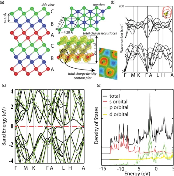
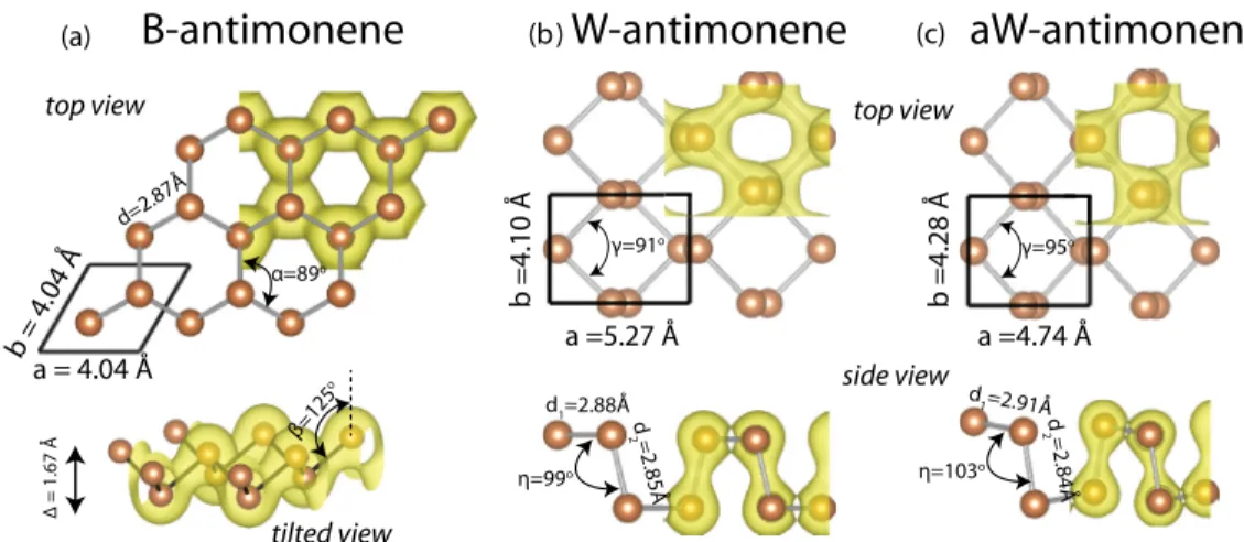
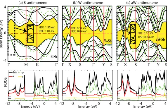
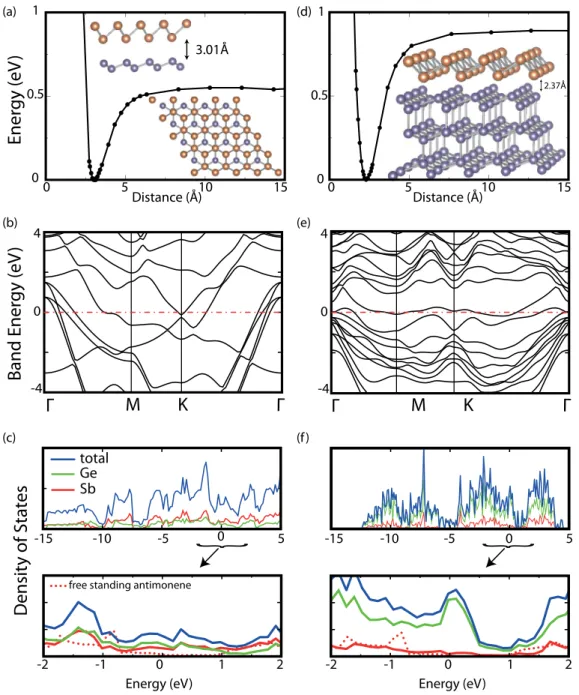
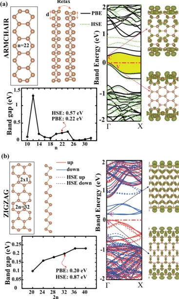
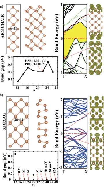
Single-layer crystalline phases of antimony: Antimonenes
Tam metin
Şekil

Benzer Belgeler
Bu bağlamda, bu araştırma, öğrencilerin, armoni eğitiminde zorluk çektikleri konular, zorluk çekmelerinin sebepleri ile bu sorunları aşabilmelerinde etkili olabilecek
Beden eğitimi ve spor yüksekokulu öğrencilerinin bölümlere göre değerlendirildiğinde beden eğitimi ve spor öğretmenliği bölümünde okuyan öğrencilerin
Onu toprağa verdik. Edebiyatımız, garb edebiyatlarının tesiri altında kal mağa başladığı zamandan bugüne ka darki devre içinde bu büyüklükte bir sima
In this paper, we build models for five main macroeconomic indicators, GDP Growth Rate, Private Saving Rate, Budget Deficit, Unemployment Rate, and Inflation, with both
In this study, we present a direct detection distributed acoustic sensor based on phase-sensitive optical time domain reflectometer (φ-OTDR) with long sensing range
Besides the principal, assistant/ department heads are responsible providing data regarding the teacher's performance outside the class (such as the teacher's attitude
30 Department of Clinical Immunology and Infectious Diseases, National Research Institute of Tuberculosis and Lung Diseases, Shahid Beheshti University of Medical Sciences,
The pairwise comparisons found that apartments dwellers were significantly different than row house and detached house dwellers regard- ing their satisfaction level both with
