M A T E R I A L S S C I E N C E
Ultrahydrophobic 3D/2D fluoroarene bilayer-based
water-resistant perovskite solar cells with efficiencies
exceeding 22%
Yuhang Liu1*, Seckin Akin1,2*, Linfeng Pan3, Ryusuke Uchida1,4, Neha Arora1, Jovana V. Milić1, Alexander Hinderhofer5, Frank Schreiber5, Alexander R. Uhl1†, Shaik M. Zakeeruddin1,
Anders Hagfeldt3, M. Ibrahim Dar1‡, Michael Grätzel1‡
Preventing the degradation of metal perovskite solar cells (PSCs) by humid air poses a substantial challenge for
their future deployment. We introduce here a two-dimensional (2D) A2PbI4 perovskite layer using
pentafluoro-phenylethylammonium (FEA) as a fluoroarene cation inserted between the 3D light-harvesting perovskite film and the hole-transporting material (HTM). The perfluorinated benzene moiety confers an ultrahydrophobic character to the spacer layer, protecting the perovskite light-harvesting material from ambient moisture while mitigating ionic diffusion in the device. Unsealed 3D/2D PSCs retain 90% of their efficiency during photovoltaic operation for 1000 hours in humid air under simulated sunlight. Remarkably, the 2D layer also enhances interfacial hole extraction, suppressing nonradiative carrier recombination and enabling a power conversion efficiency (PCE) >22%, the highest reported for 3D/2D architectures. Our new approach provides water- and heat-resistant operationally stable PSCs with a record-level PCE.
INTRODUCTION
Perovskite solar cells (PSCs) have attracted intense research interest because of their unique properties including an outstanding power conversion efficiency (PCE), tunable bandgap, low cost, and large-scale processability. In the past decade, the PSC field has witnessed a marked increase in PCE from ~3 to 23.7% (1–5). However, for large-scale practical deployment, long-term operational stability of PSCs under outdoor conditions needs to be achieved (6–10). To this end, various approaches have been used (11–14). Two-dimensional (2D) perovskites receive increasing attention as they show stronger resistance toward moisture and heat compared with their 3D analogs (15–17). However, because of their anisotropic charge transport properties, the PCE of pure 2D PSCs has remained below 14% (18, 19). To marry the desired features of 2D perovskites with the excellent light-harvesting properties of 3D PSCs, the concept of embedding low-dimensional perovskites into a 3D perovskite matrix was introduced, resulting in PCEs up to 21.06% (15, 20–22). The challenge remains to retain PCEs comparable to 3D PSCs yet achieving high photovoltaic operational stability under ambient air conditions. Ideally, this goal could be realized by achieving a precise control over the deposition of a hydrophobic, uniform, and conformal 2D layer on top of a 3D perovskite film. Because of mitigated
disper-sion forces related to the high electronegativity of fluorine (F), fluori-nated compounds are normally hydrophobic and hardly wetted by water. Mitzi and colleagues (23, 24) first prepared fluorinated tin perovskites, while lead analogs were first reported by Deleporte and colleagues (25). Mathews and colleagues (26) and Bi et al. (27) used partially fluorinated aliphatic amines for interfacial defect passivation of PSCs, while Grancini and colleagues (28, 29) explored fluorous aliphatic spacer groups within 2D perovskite materials reaching PCE up to 20% without hysteresis correction and scan speed–independent maximum power point (MPP) confirmation. Here, we demonstrate the fabrication of highly efficient bilayer 3D/2D PSCs with exceptional moisture stability by depositing pentafluoro-phenylethylammonium (FEA) lead iodide [(FEA)2PbI4], an ultra-hydrophobic 2D perovskite material, onto the 3D perovskite films. Apart from inhibiting exposure of the 3D perovskite to moisture, the perfluorinated benzene unit was introduced to fashion the electronic properties of the aromatic core, facilitating hole extraction while inhibiting interlayer ion migration.
RESULTS
Morphological and elemental analysis of 3D/2D perovskite bilayer
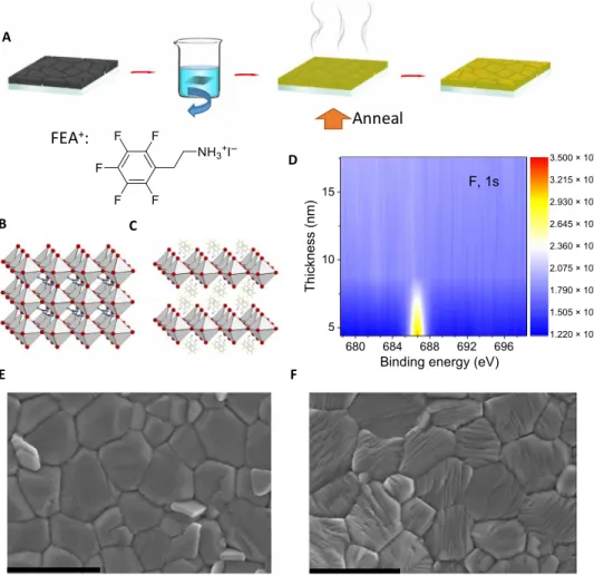
We obtain the desired architecture by immersing the 3D perovskite into a 30 mM solution of FEA iodide (FEAI) in isopropanol (IPA) followed by annealing at 120°C for 10 min. A representative scheme of our procedure and structures of the 3D and 2D perovskites is shown in Fig. 1 (A to C), respectively. The ultraviolet-visible (UV-vis) absorp-tion spectra (fig. S1) show that the FEAI treatment does not affect the absorption of the perovskite films. The top-view scanning elec-tron microscopy (SEM) images (Fig. 1, E and F) show that the FEAI treatment minimally affects the film morphology as both films are composed of perovskite domain structures with grain dimensions of ~1 m. However, the surface texture of the 3D perovskite layer treated with FEAI appears different, presumably indicating the formation
1Laboratory of Photonics and Interfaces, Department of Chemistry and
Chemi-cal Engineering, École Polytechnique Fédérale de Lausanne, Lausanne CH-1015, Switzerland. 2Department of Metallurgical and Materials Engineering, Karamanoglu
Mehmetbey University, Karaman, Turkey. 3Laboratory of Photomolecular Science,
École Polytechnique Fédérale de Lausanne, Station 6, CH-1015 Lausanne, Switzerland.
4Institute for Energy and Material Food Resources, Technology Innovation Division,
Panasonic Corporation, 3-1-1 Yagumo-naka-machi, Moriguchi City, Osaka 570-8501, Japan. 5Institut für Angewandte Physik, Universität Tübingen, 72076 Tübingen,
Germany.
*These authors contributed equally to this work.
†Present address: Laboratory for Solar Energy & Fuels, University of British Columbia, V1V 1V7 Kelowna, BC, Canada.
‡Corresponding author. Email: [email protected] (M.I.D.); michael.graetzel@ epfl.ch (M.G.)
Copyright © 2019 The Authors, some rights reserved; exclusive licensee American Association for the Advancement of Science. No claim to original U.S. Government Works. Distributed under a Creative Commons Attribution NonCommercial License 4.0 (CC BY-NC). on August 25, 2020 http://advances.sciencemag.org/ Downloaded from
S C I E N C E A D V A N C E S
|
R E S E A R C H A R T I C L E
of an overlayer. Because of the strong interaction of the ammonium iodide with the lead iodide (30), FEAI can be adsorbed on the surface and grain boundaries of the 3D perovskite films by replacing A cations or inserting into A cation vacancies. To probe the vertical and lateral distributions of FEA+ in the perovskite films, we explored elemental analysis–based techniques including x-ray photoelectron spectroscopy (XPS) depth profiling and energy-dispersive x-ray spectroscopy (EDS), respectively. As shown in Fig. 1D, the XPS depth profiling of fluorine (F) establishes the presence of FEA+ in the top ~9-nm-thin layer, whereas the EDS mapping confirms the conformal and uniform distribution of FEA+ over the 3D perovskite layer (fig. S2). The XPS analysis also shows the gradual increase in the signals corre-sponding to Pb and I, confirming the presence of the 3D perovskite layer underneath (fig. S2).
Structural characterization of 3D/2D perovskite bilayer
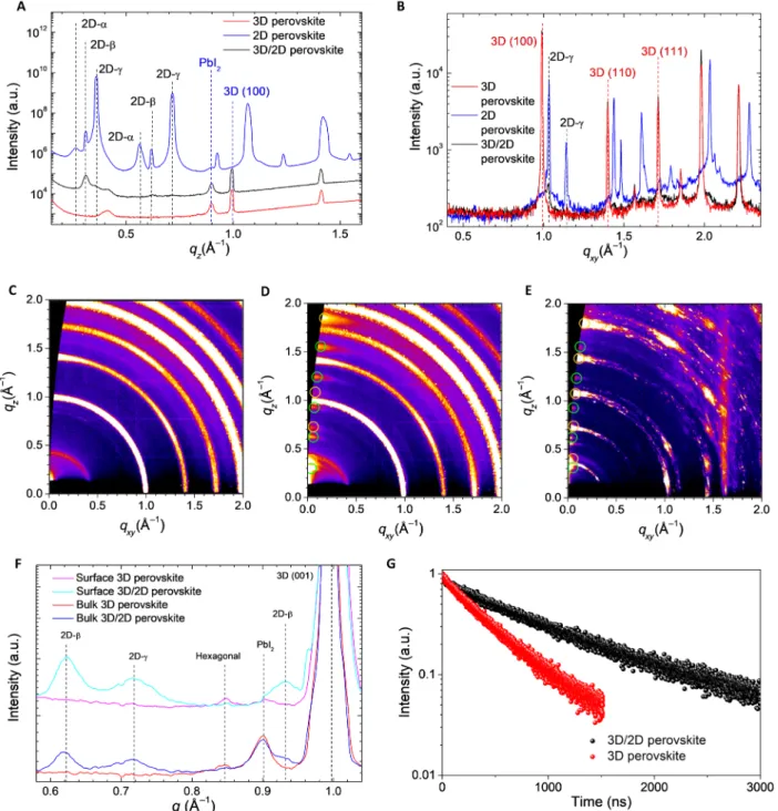
To study the structure of the thin layer containing FEA+ supported onto the 3D perovskite film, we acquired x-ray reflectivity (XRR; by which we mean specular data, i.e., the out-of-plane structure) and grazing incidence x-ray diffraction (GIXD; i.e., the in-plane struc-ture) patterns from neat and FEAI-treated 3D perovskite substrates (Fig. 2, A and B). As a reference, a pure 2D perovskite film with the
composition (FEA)2PbI4 was characterized. This film shows three series of Bragg reflections in the XRR data (Fig. 2A) with different out-of-plane lattice spacings d presumably belonging to three dif-ferent structures and denoted by 2D- (d = 17.6 Å), 2D- (d = 20.3 Å), and 2D- (d = 22.3 Å). The 2D- structure exhibits by far the most intense Bragg reflections, being several orders of magnitude more intense than the other two structures, and it is therefore likely the most abundant structure. The XRR and GIXD of the pure 3D perovskite exhibit reflections corresponding to the cubic 3D pe-rovskite phase. After FEAI treatment, Bragg reflections corre-sponding to the 3D perovskite remain unaffected. In addition, weak reflections of the 2D- and 2D- structures appear in the XRR and GIXD. The XRR pattern of the FEAI-treated 3D perovskite film is a superposition of reflections corresponding to the pure 2D and 3D perovskite systems, corroborating the successful formation of 3D/2D architecture. Because no additional reflections are observed in the XRR and GIXD patterns of the 3D/2D system, the formation of a modified unit cell can be ruled out. The crystal quality of the 3D perovskite structure, determined by peak width and intensity from the GIXD patterns (Fig. 2B), is not affected in the mixture; how-ever, the 2D crystal growth is notably altered in the 3D/2D sample compared with the pure 2D material. Estimated from the XRR peak
680 684 688 692 696 5
10 15
Binding energy (eV)
Thickness (nm) 1.220 × 10⁴ 1.505 × 10⁴ 1.790 × 10⁴ 2.075 × 10⁴ 2.360 × 10⁴ 2.645 × 10⁴ 2.930 × 10⁴ 3.215 × 10⁴ 3.500 × 10⁴ F, 1s
Fig. 1. Experimental strategy and elemental and morphological analysis of 3D/2D perovskite bilayer. (A) Schematic illustration of the 2D treatment of 3D perovskite
to form the 3D/2D bilayer perovskite with the structural representation of the FEA+ cation and the corresponding optimized geometry [density functional theory (DFT)
calculation on B3LYP/6-31G(d) level of theory]. (B and C) Structures of pure 3D perovskite and pure 2D perovskite, respectively. (D) Fluorine XPS in-depth profiling of a 3D/2D bilayer perovskite. (E and F) SEM images of a pure 3D and an FEAI-treated 3D/2D perovskite film, respectively. Scale bars, 1000 nm.
on August 25, 2020
http://advances.sciencemag.org/
width, the 2D- structure has a thickness of ~8 nm, consistent with XPS depth profiling.
Furthermore, to investigate the preferred orientation of the 2D perovskite grains laminated on the surface of the 3D perovskite, we recorded grazing incidence wide-angle x-ray scattering (GIWAXS; here, we mean the full area-detector data) data from 3D, 3D/2D, and 2D films (Fig. 2, C to E, and fig. S3). Figure 2F shows radial integration of GIWAXS data of 3D and 3D/2D perovskites, each
measured at two different angles of incidences, i.e., 0.1° (more sur-face sensitive) and 0.2° (more bulk sensitive). Both the 3D and 3D/2D materials show identical Bragg reflections and a preferred orientation for the perovskite. The 2D material (2D- and 2D-) in the 3D/2D bilayer is still textured in the out-of-plane direction, however with larger angular distribution (mosaicity). This observa-tion is consistent with the increased peak width observed in GIXD and XRR (Fig. 2, A and B). From the relative Bragg peak intensities
Fig. 2. Structural and spectroscopic characterization of 3D/2D perovskite bilayer. Structural characterizations of perovskite films. (A) XRR data of pure 2D, 3D, and
3D/2D perovskite films. a.u., arbitrary unit. (B) GIXD data of pure 2D, 3D, and 3D/2D perovskite films. The angle of incidence is 0.14°, which is slightly above the critical angle at the used x-ray energy (22 keV). (C to E) GIWAXS data of 3D, 3D/2D, and pure 2D perovskite films (angle of incidence = 0.1°). Green and orange circles denote the 2D- and 2D- structures, respectively. (F) Radially integrated intensity of GIWAXS data at two different angles of incidences to change between bulk (0.2°) and surface (0.1°) sensitivity. (G) TRPL decay traces recorded from the 3D and 3D/2D perovskite films.
on August 25, 2020
http://advances.sciencemag.org/
S C I E N C E A D V A N C E S
|
R E S E A R C H A R T I C L E
dependent on the penetration depth (Fig. 2F), we conclude that the 2D material is located dominantly at the surface of the 3D/2D bilayer, corresponding to approximately four layers of (FEA)2PbI4 derived from the overall thickness (8 nm) and the out-of-plane lattice spacing. Pure PbI2 is present mostly in the bulk but not at the surface. In addition, the amount of the hexagonal polymorph (nonperovskite phase) formed at the surface of the 3D/2D film (Fig. 2F) is substantial reduced in comparison with the 3D mate-rial. We conclude from this observation that the nonperovskite phase of FAPbI3 is consumed by the formation of the 2D material as described in the equation below
FAPbI3() + 2FEAI = (FEA)2PbI4 + FAI
Charge carrier dynamics
The potential of the 3D/2D bilayer architecture is further evaluated by investigating the emission features using steady-state and time- resolved photoluminescence (TRPL) spectroscopy. The intensity of the PL peak corresponding to band-to-band recombination is found to be fivefold higher in the 3D/2D bilayer perovskite than for the pristine 3D perovskite film, confirming the high excitonic quality of the former films (see fig. S4). In the presence of hole-transporting materials (HTMs), the PL of both 3D and 3D/2D perovskite films is strongly quenched. We estimate the PL quenching efficiency to be 92 and 99%, respectively (see fig. S4) (31), inferring that the 2D lay-er improves the extraction of holes from the light-harvesting laylay-er. The TRPL (Fig. 2G) shows more than twofold increase in the charge carrier lifetime by applying the 2D surface treatment [t10(3D/2D) = 2550 ns and t10(3D) = 950 ns], confirming the high optoelectronic quality of the 3D/2D perovskite film and a reduction in nonradiative recombination (32). The TRPL studies also show that the 3D/2D bilayer perovskite film injects holes into the HTM faster than the pristine 3D perovskite films, implying an improvement of the hole transfer process (fig. S5). This is further in accordance with the close interaction of the 3D/2D perovskite film with the HTM.
Photovoltaic characterization
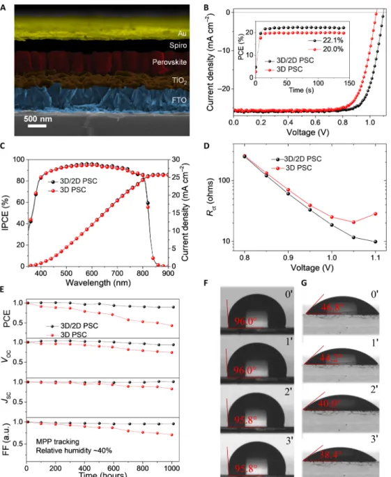
Furthermore, we investigated the influence of 2D perovskite layer on the photovoltaic performance of PSCs fabricated using fluorine- doped tin oxide (FTO)/compact TiO2 (c-TiO2)/mesoporous TiO2/ perovskite/N2,N2,N2′,N2′,N7,N7,N7′,N7′-octakis(4-methoxyphenyl)- 9,9′-spirobi[9H-fluorene]-2,2′,7,7′-tetramine (spiro-OMeTAD)/Au architecture (Fig. 3A). The current density-voltage (J-V) curves of PSCs were recorded under standard AM 1.5G illumination (100 mW cm−2), and the results are summarized in Table 1. We obtained efficiency as high as 22.2% for 3D/2D bilayer-based PSCs with an open circuit voltage (VOC) of 1.096 V, a fill factor (FF) of 78.4%, and a short circuit current (JSC) of 25.8 mA cm−2, which is the highest value reported for a PSC using 2D perovskite layers. Under similar conditions, the reference PSC yielded a PCE of 20.6% with a VOC of 1.045 V, an FF of 77.5%, and a JSC of 25.5 mA cm−2 (Fig. 3B). The photovoltaic metrics in fig. S6 depict the high repro-ducibility of PCEs in this study. We further ascertained these values by recording scan speed–independent MPP measurement (Fig. 3B) corresponding to PCEs of 20.0 and 22.1% for the 3D reference and the 3D/2D bilayer-based PSCs, respectively. For both systems, outstanding JSC up to 25.8 mA cm−2 is observed, which is in excel-lent agreement with the corresponding JSC values integrated from the incident photon-to-current efficiency (IPCE) curves (Fig. 3C).
However, the 3D/2D bilayer- based PSCs show 50 mV higher photovoltages compared with those yielded by the reference PSCs. Such an enhancement arises from the suppression of nonradiative carrier recombination at the (3D/2D)/HTM perovskite interface re-flected by the long-lasting charge carriers in the 3D/2D perovskite layer (Fig. 2G and fig. S4) (33). In addition, the charge transport resistance, extracted by fitting the high-frequency component of our electrochemical impedance spectrometry (EIS) data, is seen to be substantial reduced over the high-voltage region, i.e., above 0.8 V in the 3D/2D PSC, where the photovoltaic cell has its MPP (Fig. 3D and fig. S7). Because all other contacting layers, e.g., FTO/ TiO2/perovskite, are applied using exactly the same conditions, the difference in resistance can be assigned to an enhanced charge transport across the perovskite/HTM interface.
Operational stability under humid conditions
Last, we assessed the operational stability of the nonencapsulated devices at the MPP under 1 sun irradiation in ambient condition with a prevalent humidity of 40%. After 1000 hours, the 3D/2D bilayer PSC retained 90% of its initial efficiency, while the PCE of the pure 3D PSC dropped to 43% (Fig. 3E). We also demon-strate that the FEA- based 3D/2D PSC exhibits superior stability in the dark in a high relative humidity up to 90% (fig. S8). The excellent moisture resistance of our 3D/2D bilayer-based PSCs is attributed to the ultrahydrophobic character of the perfluorinated 2D perovskite layer, as revealed by contact angle measurements, shown in Fig. 3 (F and G). Using Neumann’s equation (see fig. S9) (34), we calculated a surface free energy of 24.3 mJ/m2 for the 3D/2D perovskite layer, which is lower than 54.7 mJ/m2 for the pristine 3D perovskite layer. Notably, the surface free energy of the 3D/2D perovskite (35) is similar to that of a pure 2D layer (23.6 mJ/m2; fig. S9). In addition to the moisture resistance, the presence of the 2D layer was also seen to improve the intrinsic sta-bility of the 3D/2D PSCs. EIS data for voltages greater than 850 mV showed the suppression of pseudo- inductive device behavior (i.e., a negative total capacitance; see fig. S7), which occurs in nonsta-tionary systems and may be related to the ion migration in the perovskite (36). The suppression of the ion migration in the 3D/2D PSC is believed to be beneficial for the device stability at an elevated temperature (see fig. S10).
DISCUSSION
We have demonstrated successful and well-controlled deposition of an ultrahydrophobic, ultrathin, and highly uniform 2D (FEA)2PbI4 layer on 3D perovskite layer. The layered (FEA)2PbI4 structure is based on the fluoroarene spacer cation, namely, FEA, featuring a terminal ammonium group for interaction with the {PbI4} layers via hydrogen bonding, which is attached to the perfluorinated benzene core through a flexible ethylene linker. Remarkably, the formation of the (FEA)2PbI4 2D layer consumes the nonperovskite phase of FAPbI3 present at the surface of 3D perovskite layer, which further brings out the novelty of our approach. In addition, the perfluo-rinated moiety strongly enhances hydrophobicity, which played a critical role in protecting the perovskite light harvester from ambient moisture. We also surmise that the intrinsic incompatibility between the hydrophilic perovskite and the hydrophobic HTM creates detri-mental charge collection losses in the device. Through the incorpo-ration of an ultrahydrophobic 2D perovskite layer between the 3D
on August 25, 2020
http://advances.sciencemag.org/
perovskite and the HTM, we mitigated these losses and improved the hole injection from the conduction band of the perovskite layer into the highest occupied molecular orbital of spiro-OMeTAD, which is also in agreement with the TRPL measurements. In conclusion,
our work provides a potential strategy to fabricate efficient PSCs with good operational stability under humid conditions, thus over-coming one of the most challenging problems associated with PSCs, i.e., extrinsic instability.
Fig. 3. Device architecture, photovoltaic performance, and operational stability of 3D/2D bilayer PSCs. (A) Cross-sectional SEM of a 3D/2D PSC. (B) I-V curves of a 3D PSC and a
3D/2D PSC, with inset showing MPP tracking. (C) IPCE curves of a 3D PSC and a 3D/2D PSC. (D) Plot of contact resistance against voltage. (E) Ambient atmosphere aging results of a 3D PSC and a 3D/2D PSC, with the relative humidity shown in the inset. (F and G) Images of water droplets on the surface of 3D/2D and 3D perovskite films at different water loading times.
Table 1. Photovoltaic parameters of 3D/2D and 3D PSCs (measured under simulated AM 1.5G solar irradiance at 100 mW cm−2).
PSC VOC (V) FF (%) JSC (mA cm−2) PCE (%) PCEMPP* (%)
3D/2D 1.096 (1.095)† 78.4 (76.9) 25.79 (25.81) 22.16 (21.70) 22.09
3D 1.045 (1.036) 77.5 (75.1) 25.47(25.47) 20.62 (19.74) 19.97
*MPP tracking. The efficiencies are recorded after 140-s MPP tracking. †The brackets indicate the average values of 25 PSC devices.
on August 25, 2020
http://advances.sciencemag.org/
S C I E N C E A D V A N C E S
|
R E S E A R C H A R T I C L E
MATERIALS AND METHODSMaterials
Lead iodide, cesium iodide, and hydrogen iodide aqueous solu-tions (57%) were purchased from TCI Co. Ltd. Formamidinium iodide, methyl ammonium iodide, and spiro-OMeTAD were pur-chased from Dyesol. Ultradry dimethylformamide (DMF), ultradry dimethyl sulfoxide (DMSO), and ultradry chlorobenzene (CB) were purchased from Acros, and dry IPA, 4-tert-butyl pyridine, lithium bistrifluorosulfonyl imide (LiTFSI), acetyl acetone, titanium diiso-propoxide bis(acetylacetonate), 75 weight % (wt %) in IPA and borane tetrahydrofuran complex solution [1.0 M in tetrahydrofuran (THF)], were purchased from Sigma-Aldrich. Pentafluorophenylace-tonitrile was purchased from Fluorochem. All the chemicals were used as received without further purification. Conductive glass, FTO (10 ohms/sq), was purchased from Nippon Sheet Glass, and tita-nium dioxide paste (30 NR-D) was purchased from Dyesol. FEAI was synthesized according to an optimized recipe from a previously reported literature (25).
Borane tetrahydrofuran complex solution (1.0 M in THF, 5 ml) was added into a solution of pentafluorophenyl acetonitrile (300 mg, 1.45 mmol) in THF (5 ml) dropwise at 0°C under the protection of argon, and the mixed solution was allowed to reflux overnight. After reduction, the resulting amine solution was treated with hydrogen iodide aqueous solution (57%, 1 ml, 7.7 mmol) and stirred at 0°C for 1 hour. The resulting brownish solution was concentrated, and the solvent was removed under reduced pressure. The resulting brown solid was washed with diethyl ether three times to yield a white crystal-line final product (420 mg, 73%).
Substrate preparation
Nippon Sheet Glass (10 ohms/sq) was consecutively cleaned using 2% Hellmanex aqueous solution, deionized water, acetone, and ethanol by sonicating for 20 min for each solvent. After drying with com-pressed air, UV-ozone was applied for further cleaning. c-TiO2 was deposited on top of FTO using the spray pyrolysis method: The sub-strates were preheated to 450°C; a precursor solution of titanium diisopropoxide bis(acetylacetonate), 75 wt % in IPA, was diluted with dry ethanol with a volume ratio of 1:9 and with the addition of 4% vol-ume ratio of additional acetyl acetone. After spray pyrolysis, the FTO/ TiO2 substrate was allowed to heat at 450°C for 30 min before cooling down to room temperature. Mesoscopic TiO2 was applied by spin coating a diluted solution of 30 NR-D paste (mass ratio of paste: EtOH = 1:6) at 4000 rpm with an acceleration of 2000 rpm/s. The as-prepared FTO/c-TiO2/TiO2 paste was then allowed to sinter at 450°C for 1 hour, yielding FTO/c-TiO2/mesoscopic TiO2, which was then deposited with perovskite freshly.
Perovskite deposition
Pure 3D perovskite precursor solution was prepared by dissolving a mixture of lead iodide (736.5 mg, 1.60 mmol), formamidinium io-dide (237.3 mg, 1.38 mmol), methylammonium ioio-dide (9.5 mg, 0.06 mmol), and cesium iodide (15.6 mg, 0.06 mmol) in 1 ml of mixed solution of DMF and DMSO [DMF (v):DMSO (v) = 4:1] under mild heating condition at ~70°C to assist dissolving. The perovskite active layer was deposited using an antisolvent method, with CB as the antisolvent. The perovskite precursor solution was deposited on the freshly prepared FTO/c-TiO2/m-TiO2 substrate, and a two-step spin-coating method was applied. The first step was carried out at 1000 rpm with an acceleration rate of 200 rpm/s for 10 s. The second
step followed at 5000 rpm with an acceleration rate of 2000 rpm/s for 20 s. CB (200 l) was applied at the 10th second. After spin coating, the substrate was allowed to anneal at 110°C for 40 min. The whole procedure was done in a nitrogen-filled glovebox.
Pure 2D perovskite film was casted from a precursor solution containing a mixture of lead iodide (461 mg, 1 mmol) and FEAI (678.1 mg, 2 mmol) in 1 ml of mixed solution of DMF and DMSO [DMF (v):DMSO (v) = 4:1] under mild heating condition at ~70°C to assist dissolving, and no antisolvent was applied during casting of the pure 2D perovskite. The same two-step spin-coating method as that used for 3D perovskite was applied, and the resulting pale yel-low film was alyel-lowed to anneal at 110°C for 10 min to yield a bright yellow film. The whole procedure was performed in a nitrogen-filled glovebox.
2D dipping treatment
The bilayer-based 2D perovskite was fabricated by postdipping treat-ment of the 3D perovskite with a solution of the 2D reagent, FEAI in IPA with a concentration of 30 mM for 10 s. The residue FEAI solution was removed by spin coating, followed by annealing treat-ment at 120°C for 10 min. The procedure was finished in a nitrogen- filled glovebox.
Hole-transporting layer
Spiro-OMeTAD was selected as a hole-transporting layer (HTL) material. Spiro-OMeTAD was dissolved in CB with a concentration of 70 mM, which was doped by LiTFSI and 4-tert-butyl pyridine, and the molar ratios were 33 and 330%, respectively. The mixed spiro- OMeTAD solution was spin casted on the surface of the perovskite at 4000 rpm for 30 s. The acceleration was 2000 rpm/s.
Gold electrode and antireflective coating
The gold electrode was thermally evaporated on the surface of the HTL with the shadow mask with an area of 5 mm by 5 mm. The thickness of the gold electrode was 80 nm, and the evaporation speed was adjusted to 0.01 nm/s at the first 10 nm and to 0.08 nm/s for the rest of the procedure. A thin layer of magnesium fluoride (MgF2) was coated on the top electrode of the cells with an E-beam evaporator under room temperature. The thickness of the MgF2 layer was opti-mized to 140 nm.
Photovoltaic performance measurements
After finishing the gold evaporation and antireflective coating, the solar cells were measured using a 300-W Xenon light source from Oriel. The spectral mismatch between AM 1.5G and the solar simu-lator was calibrated by a Schott K113 Tempax filter (Prazosopms Glas & Optik GmbH). A silicon photodiode was used as light inten-sity calibrator for each measurement. Keithley 2400 was used for the current-voltage scan by applying an external voltage bias and mea-suring the response current with a scan rate of 50 mV/s. The cells were masked with a black metal mask with an area of 0.16 cm2. IPCE was recorded with a commercial apparatus (Aekeo-Ariadne, Cicci Research s.r.l.) based on a 300-W Xenon lamp. Stability of the cells was measured under a white light-emitting diode lamp with biologic MPG2 potentiostat and was performed under open air. The device area was masked to around 0.13 cm2. The spectral mismatch between AM 1.5G and the solar simulator was calibrated by a Schott K113 Tempax filter, whose light intensity was calibrated with a silicon diode. The light intensity was around 83 mW cm−2, and the actual
on August 25, 2020
http://advances.sciencemag.org/
current was adjusted according to in-time calibration result from the silicon diode. The stability data were acquired from the MPP track-ing of a nonencapsulated device exposed to open air. The relative humidity of the ambient atmosphere varies from 40 to 60%. Upon higher humidity level, a mild nitrogen flow was applied to adjust the humidity to ~40%. Relative humidity was monitored by Sigma- Aldrich Humidity/Temperature Pen 445580.
Structural characterizations
X-ray scattering experiments were done at beamline ID10 EH1 of the European Synchrotron Radiation Facility (ESRF) with a photon energy of 22 keV under nitrogen atmosphere. The beam size was 10 m in the vertical direction and 120 m in the horizontal direc-tion. GIXD data were measured under an angle of incidence of 0.08° with a point detector. GIWAXS data were measured with a PILATUS 300 k area detector under the same angle of incidence.
SEM and XPS measurements
XPS measurements were performed with a PHI VersaProbe II scan-ning XPS microprobe using a monochromatic Al K x-ray of 24.8-W power with a beam size of 100 m. Core-level signals were obtained at 45° take-off angle. All peaks were calibrated using C 1s peak at 284.8 eV to correct charge shift of binding energies. Curve fitting was performed using the PHI MultiPak software. Depth profiling etching speed was calibrated using Si as standard. The top-view and cross- sectional morphologies of the films were characterized using a high- resolution scanning electron microscope (Zeiss Merlin) with an in-lens detector.
Contact angle measurement
The hydrophilicity of surfaces as a function of time was assessed by contact angle measurement by a drop shape analyzer (KRÜSS, DSA100) at ambient temperature.
PL, TRPL, and UV-vis measurements
UV-vis absorptions were measured using a Varian Cary 500 spec-trometer (Varian, USA). Steady-state PL was measured using an Edinburgh Instruments FLS920P fluorescence spectrometer, and for PL life time measurement [time-correlated single-photon counting (TCSPC)], a picosecond pulse diode laser (EPL-405; excitation wave-length, 405 nm; pulse width, 49 ps) was used.
Impedance measurements
The device behavior was characterized by EIS in the dark at a frequency range of 500 kHz to 100 mHz using a Bio-Logic SP300 potentiostat and a Faraday cage. Completed devices with an FTO/ blocking TiO2/mesoporous TiO2/perovskite/spiro-OMeTAD/Au architecture were used for the measurement. Devices were exposed to forward bias potentials from 0 to 1.1 V in steps of 0.05 V on which a sinusoidal perturbation of 20 mV was superimposed. ZView v.2.80 (Scribner Associates Inc.) was used to perform data analysis and equivalent circuit fitting of EIS data in Nyquist plot representation.
DFT calculations
Density functional theory (DFT) calculations were conducted with the Gaussian 16 Revision A.03 suite of programs (37, 38), which was carried out on the Fidis computer cluster of École Polytechnique Fédérale de Lausanne (EPFL). The geometry optimization was per-formed at the B3LYP/6-31G(d) level of theory.
SUPPLEMENTARY MATERIALS
Supplementary material for this article is available at http://advances.sciencemag.org/cgi/ content/full/5/6/eaaw2543/DC1
Fig. S1. UV-vis absorption spectrum of 3D and 3D/2D perovskite films and geometry of FEA+
cation.
Fig. S2. Surface and in-depth elemental analyses of 3D/2D perovskite bilayer.
Fig. S3. Cross-comparison of the GIWAXS patterns on surface and in bulk for 3D and 3D/2D perovskites, respectively.
Fig. S4. Steady-state PL of 3D and 3D/2D perovskite systems.
Fig. S5. Hole injection dynamics and band diagram of the 3D/2D perovskite system.
Fig. S6. JSC, VOC, FF, and PCE distributions of 50 devices, in which 25 devices are 3D/2D PSCs
and 25 are 3D PSCs.
Fig. S7. Impedance spectroscopy and capacitance measurement of 3D and 3D/2D PSCs. Fig. S8. Water and humidity resistance of 3D/2D and 3D PSCs.
Fig. S9. Image of water droplet on the surface of pure 2D [(FEAI)2PbI4] perovskite films.
Fig. S10. Stability of a 3D/2D PSC and a 3D PSC at an elevated temperature. REFERENCES AND NOTES
1. NREL, Best research efficiencies; www.nrel.gov/pv/assets/pdfs/pv-efficiency-chart.20190103.pdf.
2. A. Kojima, K. Teshima, Y. Shirai, T. Miyasaka, Organometal halide perovskites as visible-light sensitizers for photovoltaic cells. J. Am. Chem. Soc. 131, 6050–6051 (2009). 3. D. Bi, C. Yi, J. Luo, J.-D. Décoppet, F. Zhang, S. M. Zakeeruddin, X. Li, A. Hagfeldt,
M. Grätzel, Polymer-templated nucleation and crystal growth of perovskite films for solar cells with efficiency greater than 21%. Nat. Energy 1, 16142 (2016).
4. W. S. Yang, B.-W. Park, E. H. Jung, N. J. Jeon, Y. C. Kim, D. U. Lee, S. S. Shin, J. Seo, E. K. Kim, J. H. Noh, S. I. Seok, Iodide management in formamidinium-lead-halide–based perovskite layers for efficient solar cells. Science 356, 1376–1379 (2017).
5. Y. Zhao, K. Zhu, Organic–inorganic hybrid lead halide perovskites for optoelectronic and electronic applications. Chem. Soc. Rev. 45, 655–689 (2016).
6. Y. Rong, Y. Hu, A. Mei, H. Tan, M. I. Saidaminov, S. I. Seok, M. D. McGehee, E. H. Sargent, H. Han, Challenges for commercializing perovskite solar cells. Science 361, eaat8235 (2018).
7. J. Burschka, N. Pellet, S.-J. Moon, R. Humphry-Baker, P. Gao, M. K. Nazeeruddin, M. Grätzel, Sequential deposition as a route to high-performance perovskite-sensitized solar cells. Nature 499, 316–319 (2013).
8. N. J. Jeon, J. H. Noh, W. S. Yang, Y. C. Kim, S. Ryu, J. Seo, S. I. Seok, Compositional engineering of perovskite materials for high-performance solar cells. Nature 517, 476–480 (2015).
9. M. M. Lee, J. Teuscher, T. Miyasaka, T. N. Murakami, H. J. Snaith, Efficient hybrid solar cells based on meso-superstructured organometal halide perovskites. Science 338, 643–647 (2012).
10. H.-S. Kim, C.-R. Lee, J.-H. Im, K.-B. Lee, T. Moehl, A. Marchioro, S.-J. Moon, R. Humphry-Baker, J.-H. Yum, J. E. Moser, M. Grätzel, N.-G. Park, Lead iodide perovskite sensitized all-solid-state submicron thin film mesoscopic solar cell with efficiency exceeding 9%. Sci. Rep. 2, 591 (2012).
11. T. Leijtens, G. E. Eperon, N. K. Noel, S. N. Habisreutinger, A. Petrozza, H. J. Snaith, Stability of metal halide perovskite solar cells. Adv. Energy Mater. 5, 1500963 (2015).
12. A. J. Pearson, G. E. Eperon, P. E. Hopkinson, S. N. Habisreutinger, J. T.-W. Wang,
H. J. Snaith, N. C. Greenham, Oxygen degradation in mesoporous Al2O3/CH3NH3PbI3-xClx
perovskite solar cells: Kinetics and mechanisms. Adv. Energy Mater. 6, 1600014 (2016).
13. N. Arora, M. I. Dar, A. Hinderhofer, N. Pellet, F. Schreiber, S. M. Zakeeruddin, M. Grätzel, Perovskite solar cells with CuSCN hole extraction layers yield stabilized efficiencies greater than 20%. Science 358, 768–771 (2017).
14. A. Mei, X. Li, L. Liu, Z. Ku, T. Liu, Y. Rong, M. Xu, M. Hu, J. Chen, Y. Yang, M. Grätzel, H. Han, A hole-conductor–free, fully printable mesoscopic perovskite solar cell with high stability. Science 345, 295–298 (2014).
15. H. Tsai, W. Nie, J.-C. Blancon, C. C. Stoumpos, R. Asadpour, B. Harutyunyan, A. J. Neukirch, R. Verduzco, J. J. Crochet, S. Tretiak, L. Pedesseau, J. Even, M. A. Alam, G. Gupta, J. Lou, P. M. Ajayan, M. J. Bedzyk, M. G. Kanatzidis, A. D. Mohite, High-efficiency two-dimensional ruddlesden-popper perovskite solar cells. Nature 536, 312–316 (2016).
16. I. C. Smith, E. T. Hoke, D. Solis-Ibarra, M. D. McGehee, H. I. Karunadasa, A layered hybrid perovskite solar-cell absorber with enhanced moisture stability. Angew. Chem. 126, 11414–11417 (2014).
17. G. Grancini, C. Roldán-Carmona, I. Zimmermann, E. Mosconi, X. Lee, D. Martineau, S. Narbey, F. Oswald, F. De Angelis, M. Graetzel, One-year stable perovskite solar cells by 2D/3D interface engineering. Nat. Commun. 8, 15684 (2017).
18. J.-C. Blancon, H. Tsai, W. Nie, C. C. Stoumpos, L. Pedesseau, C. Katan, M. Kepenekian, C. M. M. Soe, K. Appavoo, M. Y. Sfeir, Extremely efficient internal exciton dissociation through edge states in layered 2D perovskites. Science 355, 1288–1292 (2017).
on August 25, 2020
http://advances.sciencemag.org/
S C I E N C E A D V A N C E S
|
R E S E A R C H A R T I C L E
19. Y. Chen, Y. Sun, J. Peng, W. Zhang, X. Su, K. Zheng, T. Pullerits, Z. Liang, Tailoring organiccation of 2D air-stable organometal halide perovskites for highly efficient planar solar cells. Adv. Energy Mater. 7, 1700162 (2017).
20. T. Zhang, M. I. Dar, G. Li, F. Xu, N. Guo, M. Grätzel, Y. Zhao, Bication lead iodide 2D
perovskite component to stabilize inorganic -CsPbI3 perovskite phase for
high-efficiency solar cells. Sci. Adv. 3, e1700841 (2017).
21. Z. Wang, Q. Lin, F. P. Chmiel, N. Sakai, L. M. Herz, H. J. Snaith, Efficient ambient-air-stable solar cells with 2D–3D heterostructured butylammonium-caesium-formamidinium lead halide perovskites. Nat. Energy 2, 17135 (2017).
22. J.-W. Lee, Z. Dai, T.-H. Han, C. Choi, S.-Y. Chang, S.-J. Lee, N. de Marco, H. Zhao, P. Sun, Y. Huang, Y. Yang, 2D perovskite stabilized phase-pure formamidinium perovskite solar cells. Nat. Commun. 9, 3021 (2018).
23. D. B. Mitzi, D. R. Medeiros, P. R. L. Malenfant, Intercalated organic−inorganic perovskites stabilized by fluoroaryl− aryl interactions. Inorg. Chem. 41, 2134–2145 (2002).
24. Z. Xu, D. B. Mitzi, SnI42--based hybrid perovskites templated by multiple organic cations:
Combining organic functionalities through noncovalent interactions. Chem. Mater. 15, 3632–3637 (2003).
25. Y. Wei, P. Audebert, L. Galmiche, J.-S. Lauret, E. Deleporte, Synthesis, optical properties
and photostability of novel fluorinated organic–inorganic hybrid (R–NH3)2PbX4
semiconductors. J. Phys. D. Appl. Phys. 46, 135105 (2013).
26. K. M. M. Salim, T. M. Koh, D. Bahulayan, P. C. Harikesh, N. F. Jamaludin, B. Febriansyah, A. Bruno, S. Mhaisalkar, N. Mathews, Extended absorption window and improved stability of cesium-based triple-cation perovskite solar cells passivated with perfluorinated organics. ACS Energy Lett. 3, 1068–1076 (2018).
27. D. Bi, P. Gao, R. Scopelliti, E. Oveisi, J. Luo, M. Grätzel, A. Hagfeldt, M. K. Nazeeruddin, High-performance perovskite solar cells with enhanced environmental stability based
on amphiphile-modified CH3NH3PbI3. Adv. Mater. 28, 2910–2915 (2016).
28. K. T. Cho, Y. Zhang, S. Orlandi, M. Cavazzini, I. Zimmermann, A. Lesch, N. Tabet, G. Pozzi, G. Grancini, M. K. Nazeeruddin, Water-repellent low-dimensional fluorous perovskite as interfacial coating for 20% efficient solar cells. Nano Lett. 18, 5467–5474 (2018).
29. I. García-Benito, C. Quarti, V. I. E. Queloz, S. Orlandi, I. Zimmermann, M. Cavazzini, A. Lesch, S. Marras, D. Beljonne, G. Pozzi, M. K. Nazeeruddin, G. Grancini, Fashioning fluorous organic spacers for tunable and stable layered hybrid perovskites. Chem. Mater.
30, 8211–8220 (2018).
30. D. Luo, W. Yang, Z. Wang, A. Sadhanala, Q. Hu, R. Su, R. Shivanna, G. F. Trindade, J. F. Watts, Z. Xu, T. Liu, K. Chen, F. Ye, P. Wu, L. Zhao, J. Wu, Y. Tu, Y. Zhang, X. Yang, W. Zhang, R. H. Friend, Q. Gong, H. J. Snaith, R. Zhu, Enhanced photovoltage for inverted planar heterojunction perovskite solar cells. Science 360, 1442–1446 (2018).
31. P. Docampo, J. M. Ball, M. Darwich, G. E. Eperon, H. J. Snaith, Efficient organometal trihalide perovskite planar-heterojunction solar cells on flexible polymer substrates. Nat. Commun. 4, 2761 (2013).
32. M. I. Dar, G. Jacopin, S. Meloni, A. Mattoni, N. Arora, A. Boziki, S. M. Zakeeruddin, U. Rothlisberger, M. Grätzel, Origin of unusual bandgap shift and dual emission in organic-inorganic lead halide perovskites. Sci. Adv. 2, e1601156 (2016). 33. W. Tress, N. Marinova, O. Inganäs, M. K. Nazeeruddin, S. M. Zakeeruddin, M. Graetzel,
Predicting the open-circuit voltage of CH3NH3PbI3 perovskite solar cells using
electroluminescence and photovoltaic quantum efficiency spectra: The role of radiative and non-radiative recombination. Adv. Energy Mater. 5, 1400812 (2015).
34. L. M. Matuana, J. J. Balatinecz, C. B. Park, Effect of surface properties on the adhesion between PVC and wood veneer laminates. Polym. Eng. Sci. 38, 765–773 (1998). 35. N. Arora, M. I. Dar, M. Abdi-Jalebi, F. Giordano, N. Pellet, G. Jacopin, R. H. Friend,
S. M. Zakeeruddin, M. Grätzel, Intrinsic and extrinsic stability of formamidinium lead bromide perovskite solar cells yielding high photovoltage. Nano Lett. 16, 7155–7162 (2016).
36. C. A. Schiller, F. Richter, E. Gülzow, N. Wagner, Relaxation impedance as a model for the deactivation mechanism of fuel cells due to carbon monoxide poisoning. Phys. Chem. Chem. Phys. 3, 2113–2116 (2001).
37. J. B. Foresman, Æ. Frisch, Exploring Chemistry with Electronic Structure methods: A Guide to Using Gaussian (Gaussian Inc., ed. 2, 1996).
38. M. Frisch, G. Trucks, H. Schlegel, G. Scuseria, M. Robb, J. Cheeseman, G. Scalmani, V. Barone, G. Petersson, H. Nakatsuji, X. Li, M. Caricato, A. V. Marenich, J. Bloino, B. G. Janesko, R. Gomperts, B. Mennucci, H. P. Hratchian, J. V. Ortiz, A. F. Izmaylov, J. L. Sonnenberg, D Williams-Young, F. Ding, F. Lipparini, F. Egidi, J. Goings, B. Peng, A. Petrone, T. Henderson, D. Ranasinghe, V. G. Zakrzewski, J. Gao, N. Rega, G. Zheng, W. Liang, M. Hada, M. Ehara, K. Toyota, R. Fukuda, J. Hasegawa, M. Ishida, T. Nakajima, Y. Honda, O. Kitao, H. Nakai, T. Vreven, K. Throssell, J. A. Montgomery Jr., J. E. Peralta, F. Ogliaro, M. J. Bearpark, J. J. Heyd, E. N. Brothers, K. N. Kudin, V. N. Staroverov, T. A. Keith, R. Kobayashi, J. Normand, K. Raghavachari, A. P. Rendell, J. C. Burant, S. S. Iyengar, J. Tomasi, M. Cossi, J. M. Millam, M. Klene, C. Adamo, R. Cammi, J. W. Ochterski, R. L. Martin, K. Morokuma, O. Farkas, J. B. Foresman, D. J. Fox, Gaussian 16, revision a. 03 (Gaussian Inc., 2016).
Acknowledgments: We acknowledge the ESRF for provision of synchrotron radiation and
A. Chumakov for assistance in using beamline ID10. We thank A. Greco for support during the synchrotron beamtime, Z. Wang for assistance in the initial XRD experiment, N. Lucie for help in the EDX analysis, and P. Mettraux for the XPS experiments and analysis. Funding: Y.L., S.M.Z., and M.G. thank the King Abdulaziz City for Science and Technology (KACST) for the financial support. N.A. acknowledges the financial support from GreatCell Solar. S.A. thanks the TUBITAK 2214-A International Doctoral Research Fellowship Programme for supporting his researches at EPFL. M.I.D acknowledges the financial support from the Swiss National Science Foundation (SNSF) under project number P300P2_174471. A.R.U. acknowledges the financial support from the SNSF under project number P3P3P2_177790. J.V.M., S.M.Z., and M.G. are grateful to the SNSF for the financial support of the joint project IZLRZ2_164061 under the Scientific & Technological Cooperation Program Switzerland-Russia and the European Union's Horizon 2020 research and innovation program (under grant agreement no. 687008, GOTSolar). Author contributions: Y.L. and M.G. conceived the idea of the work. Y.L. designed the project. Y.L. designed the molecule with contribution from J.V.M. Y.L., S.A., and R.U. fabricated and characterized the devices. L.P. performed the XPS and SEM measurements and analyses. A.R.U. performed the impedance measurements and analyzed the contact angle measurement data. M.I.D., N.A., A.Hi., and F.S. recorded, analyzed, and discussed the XRD data. M.I.D. recorded and discussed the TRPL data. S.A. and Y.L. performed the contact angle and aging measurements. Y.L. and M.I.D. wrote the manuscript, and all the authors contributed toward finalizing the draft. S.M.Z. and A.Ha. helped with the coordination of the project. M.G. directed and supervised the research. Competing interests: The authors declare that they have no competing interests. Data and materials availability: All data needed to evaluate the conclusions in the paper are present in the paper and/or the Supplementary Materials. Data and materials may be requested from Y.L. (first author) and M.I.D. and M.G. (corresponding authors).
Submitted 3 December 2018 Accepted 2 May 2019 Published 7 June 2019 10.1126/sciadv.aaw2543
Citation: Y. Liu, S. Akin, L. Pan, R. Uchida, N. Arora, J. V. Milić, A. Hinderhofer, F. Schreiber, A. R. Uhl, S. M. Zakeeruddin, A. Hagfeldt, M. I. Dar, M. Grätzel, Ultrahydrophobic 3D/2D fluoroarene bilayer-based water-resistant perovskite solar cells with efficiencies exceeding 22%. Sci. Adv. 5, eaaw2543 (2019).
on August 25, 2020
http://advances.sciencemag.org/
Alexander R. Uhl, Shaik M. Zakeeruddin, Anders Hagfeldt, M. Ibrahim Dar and Michael Grätzel
DOI: 10.1126/sciadv.aaw2543 (6), eaaw2543. 5
Sci Adv
ARTICLE TOOLS http://advances.sciencemag.org/content/5/6/eaaw2543
MATERIALS
SUPPLEMENTARY http://advances.sciencemag.org/content/suppl/2019/06/03/5.6.eaaw2543.DC1
REFERENCES
http://advances.sciencemag.org/content/5/6/eaaw2543#BIBL
This article cites 35 articles, 9 of which you can access for free
PERMISSIONS http://www.sciencemag.org/help/reprints-and-permissions
Terms of Service
Use of this article is subject to the
is a registered trademark of AAAS.
Science Advances
York Avenue NW, Washington, DC 20005. The title
(ISSN 2375-2548) is published by the American Association for the Advancement of Science, 1200 New
Science Advances
License 4.0 (CC BY-NC).
Science. No claim to original U.S. Government Works. Distributed under a Creative Commons Attribution NonCommercial Copyright © 2019 The Authors, some rights reserved; exclusive licensee American Association for the Advancement of
on August 25, 2020
http://advances.sciencemag.org/