TOBB UNIVERSITY OF ECONOMICS AND TECHNOLOGY GRADUATE SCHOOL OF SCIENCE AND ENGINEERING
APPLICATION OF EFFICIENT PHOTOELECTRODES PREPARED BY CHALCOGENIDE NANOPARTICLE AND CESIUM LEAD BROMIDE PEROVSKITE SENSITIZED 3D-ZNO
NANOSTRUCTURE IN PHOTOELECTROCHEMICAL SOLAR CELLS
MASTER OF SCIENCE THESIS Mehrdad FARAJI
Department of Micro and Nanotechnology
Thesis Supervisor: Prof. Dr. Nurdan DEMIRCI SANKIR
iii
Approval of the Graduate School of Science and Technology
……… Prof. Dr. Osman Eroğul
Director I certify that this thesis meets all the requirements of the master's degree.
……… Prof. Dr. Nurdan Demirci Sankir
Head of Department Mehrdad Faraji, a M.Sc. student of TOBB University of Economics and Technology Graduate School of Engineering and Science Student ID 171611027, successfully defended the thesis entitled “APPLICATION OF EFFICIENT PHOTOELECTRODES PREPARED BY CHALCOGENIDE NANOPARTICLE AND CESIUM LEAD BROMIDE PEROVSKITE SENSITIZED 3D-ZNO NANOSTRUCTURE IN PHOTOELECTROCHEMICAL SOLAR CELLS”, which he prepared after fulfilling the requirements specified in the associated legislations, before the jury whose signatures are below.
Thesis Supervisor: Prof. Dr. Nurdan Demirci Sankir ……… TOBB University of Economics and Technology
Jury Member: Prof. Dr. Mehmet Parlak (Head) ……… Middle East Technical University
Dr. Ogr. Uyesi Zeynep Tutumlu ……… TOBB University of Economics and Technology
Prof. Dr. Nurdan Demirci Sankir ……… TOBB University of Economics and Technology
v
THESIS NOTIFICATION
I hereby declare that all the information provided in this thesis has been obtained with rules of ethical and academic conduct and has been written in accordance with thesis format regulations. I also declare that, as required by these rules and conduct, I have fully cited and referenced all material and results that are not original to this work.
vii
ÖZET
FOTOELEKTROKEMİK GÜNEŞ HÜCRELERİNDEKİ KOLOJENİD NANOPARTİKLE VE
CESIUM LEAD BROMİD PEROVSKİT SENSİTİZ 3D-ZNO NANOSTRUCTURE'İN
HAZIRLAYAN ETKİLİ FOTOELEKTROD UYGULAMALARI
Mehrdad Faraji
TOBB Ekonomi ve Teknoloji Üniversitesi
Fen Bilimleri Enstitüsü
Mikro ve Nanoteknoloji
Danışman: Prof.Dr. Nurdan Demirci Sankır
Tarih: Aralık 2019
Bu tezde, kimyasal banyo biriktirme (CBD) yöntemi kullanılarak flor katkılı kalay oksit (FTO) kaplı cam üzerine çiçek ve denizkestanesi benzeri üç boyutlu (3D) morfolojileri olan çinko oksit (ZnO) tabakaları büyütülmüştür. Daha sonra 3D-ZnO üzerine aynı yöntemle nanoyapılı kadmiyum sülfür (CdS) ve kadmiyum selenür (CdSe) tabakası büyütülmüştür. CdS ve CdSe kalkojen yapılara ek olarak, hazırlanan tezde ZnO nanoyapıların kurşun bromür perovskit (CsPbBr3) ile heteroeklemlerinin oluşturulması üzerine çalışılmıştır. Tüm bu heteroeklem yapılar, fotoelektrokimyasal güneş pillerinde fotoaktif elektrot olarak kullanılmıştır. Tez kapsamında CdSe ve CdS katmanlarını optimize etmek için ZnO / CdSe ve ZnO / CdS / CdSe yapısı 200 ° C'de 2 saat termal tavlama işlemine tabi tutularak performanslarının arttığı saptanmıştır. Üretilen tüm yapılar X-ışını fotoelektron spektroskopisi (XPS), x-ışını kırınım spektroskopisi (XRD), Uv-vis ve fotoluminesans (PL) spektroskopileri, kullanılarak analiz edilmiştir. Bunlara ek olarak üretilen morfolojiler ve kompozisyonları taramalı elektron mikroskopisi (SEM), geçirimli elektron mikroskopisi (TEM) ve enerji dağıtıcı X-ışını (EDX) ile analiz edilmiştir. İncefilmlerin başarı ile büyütüldüğü bu analizler sonucunda kanıtlanmış ve elde edilen buğuların literatüre paralel olduğu görülmüştür.
Son olarak sentezlenen yapılar fotoelektrokimyasal güneş pili su ayırma sisteminde fotoanot olarak kullanılmıştır. Bu sistemin ana amacı güneş ışığını kullanarak suyun elektroliz edilmesi ve hidrojen üretilmesidir. Çıplak ZnO ve ZnO-CdS-CdSe elektrotlarının dış kuantum verimliliği (IPCE) sırasıyla %12 ve %51 olarak hesaplanmıştır. Ayrıca, ZnO-CsPbBr3 fotoelektrotların maksimum IPCE'si yaklaşık % 37 olduğu saptanmıştır. Bu veriler, çalışmamızda hazırlanan heteroeklem bazlı elektrotların, güneş enerjisi kullanılarak su ayrıştırılması sistemlerinde kullanmaları için çok ümit verici olduğunu göstermiştir.
ix
ABSTRACT
APPLICATION OF EFFICIENT PHOTOELECTRODES PREPARED BY CHALCOGENIDE
NANOPARTICLE AND CESIUM LEAD BROMIDE PEROVSKITE SENSITIZED 3D-ZNO
NANOSTRUCTURE IN PHOTOELECTROCHEMICAL SOLAR CELLS
Mehrdad Faraji
TOBB University of Economics and Technology
Graduate School of Science and Technology
Micro and Nanotechnology
Thesis Advisor: Prof. Dr. Nurdan Demirci Sankir
Date: December 2019
In this thesis, nanostructured zinc oxide (ZnO) layer with flower and urchin-like 3D morphologies have been deposited on fluorine-doped tin oxide (FTO) coated glass using chemical bath deposition (CBD) method. Then a thin layer of nanostructured cadmium sulfide (CdS) and selenide (CdSe) have been deposited on 3D ZnO with the same method. Additionally, a lead bromide perovskite (CsPbBr3) layer structure has been fabricated on the ZnO layer via spin coating method with the aim of the utilization of these material in to photoelectrochemical water splitting device as photo anode. Moreover, to modify the cadmium selenide layers, two ZnO/CdSe and ZnO/CdS/CdSe structures have been treated by thermal annealing at 200o C for 2 hours. As a result, the crystalline structure of the photoanodes was modified significantly. The structures also were analyzed using X-ray photoelectron spectroscopy (XPS), x-ray diffraction patters (XRD), Uv-vis and photoluminescence (PL) spectroscopies, finally the morphologies and compositions were analyzed with scanning electron microscopy (SEM) and transmission electron microscopy (TEM), and energy dispersive X-ray (EDX). The substrates were proven by the mentioned analysis and compared with other works in literature.
Then the synthesized structures were used as photoanode in the photoelectrochemical solar cell water splitting system. The aim of the system was the production of hydrogen from splitting water molecules using sunlight. The incident photon-to-charge carrier efficiency (IPCE) efficiency of the bare ZnO and ZnO-CdS-CdSe electrodes have been calculated as 12% and %51, respectively. Moreover, the maximum IPCE of the ZnO-CsPbBr3 photoelectrode was approximately 37%. These data indicated that the heterojunction based electrodes prepared in this study are very promising in order to utilize them into solar water splitting systems.
xi
ACKNOWLEDGEMENT
Thanks God, which created everything and lead us to the best targets, I would
like to express my gratitude to my leader Imam Al-Mahdi the best leader of
societies. I believe that my father’s soul and older brother’s soul become happy
by seeing my successes in my life. I would like to thank my lovely mother and
sister for their help and wisely advisors for overcoming difficulties. Thanks to
dear Prof. Dr. Nurdan Demirci Sankir and Prof. Dr. Mehmet Sankir for their
supports and scientific advisors which led this M.Sc. thesis to complete. And also
thanks to TOBB University of Economics and Technology for M.Sc. scholarship
and financial supports.
December 2019 Mehrdad Faraji
(Nano Scientist)
xiii
CONTENTS
Pages ÖZET ... vii ABSTRACT ... ix ACKNOWLEDGEMENT ... xi CONTENTS ... xiiiLIST OF FIGURES ... xvii
LIST OF TABLES ... xxi
LIST OF ABBREVIATIONS ... xxiii
LIST OF SYMBOLS ... xxv
1. INTRODUCTION ... 1
1.1. Technology of Thin Film ...1
1.2. Zinc Oxide ...2
1.2.1. Growth methods ...3
1.2.2. Stability of ZnO ...3
1.2.3. Post growth treatment ...4
1.2.4. Properties of ZnO ...4
1.2.4.1. Electronic and optical properties ...4
1.2.4.2. Catalytic properties ...6
1.2.4.3. Hydrophobicity of the ZnO ...6
1.2.4.4. ZnO field emission characterization ...7
1.2.4.5. Photonic crystals ...9
1.2.4.6. Photoluminescence (PL) of ZnO ... 10
1.2.5. Applications of nanostructured ZnO ... 11
1.2.5.1. Electrochromic displays ... 11
1.2.5.2. ZnO structure in field-effect transistors ... 12
1.2.5.3. Sensors ... 13
1.2.5.4. Solar cells applications of ZnO ... 15
1.2.5.5. Hydrogen generation via water splitting ... 16
1.3. Cadmium Chalcogenide Nanostructures ... 17
1.3.1. Cadmium sulphide (CdS) ... 18
xiv
1.3.3. Synthesis of chalcogenide nanostructures ... 18
1.3.3.1. Colloidal synthesis method ... 19
1.3.3.2. High temperature injection ... 20
1.3.3.3. Hydrothermal/Solvothermal process ... 21
1.3.3.4. Microwave irradiation-assisted synthesis ... 22
1.3.3.5. Sonochemical process... 22
1.3.3.6. Capping-Assisted synthesis ... 23
1.3.4. Applications of metal chalcogenide nanostructures ... 23
1.4. Halide Perovskites ... 24
1.4.1. Properties of perovskites ... 27
1.4.2. Perovskite nanostructure synthesis ... 29
1.4.3. Applications of nanostructure perovskites ... 29
1.4.3.1. Photovoltaics applications of perovskites ... 29
1.4.3.2. Application beyond photovoltaic ... 31
1.4.3.2.1. Photodetectors ... 31
1.4.3.2.2. Light emitting diodes (LEDs) and laser ... 33
1.5. Principles of Photoelectrochemical (PEC) Cells ... 35
1.5.1. Thermodynamics of photoelectrochemical and photocatalytic water splitting ... 36
2. SYNTHESIS AND CHARACTERIZATION OF FABRICATED SEMICONDUCTOR ... 39
2.1. Chemical Synthesis of Nanostructured Thin Film ... 39
2.2. Chemical Bath Deposition (CBD) Synthesis Method ... 39
2.3. Synthesis of the Nanostructured Thin Film Via Spin Coating ... 40
2.4. Experimental Semiconductor Synthesis ... 41
2.4.1. Nanostructured ZnO ... 41
2.4.2. ZnO/CdS structure fabrication ... 42
2.4.3. ZnO/CdSe and ZnO/CdS/CdSe structures synthesis ... 43
2.4.4. ZnO/CsPbBr3 structure synthesis ... 44
2.5. Thermally Post Treatment of the ZnO/CdS/CdSe and ZnO/CdSe Structures ... 45
2.6. Photoelectrochemical (PEC) System and Electrolyte ... 46
2.7. Photoluminescence (PL) and Absorbance Spectroscopy of The Structures ... 46
2.8. X-ray Photoelectron Spectroscopy (XPS) ... 47
xv
2.10. Scanning Electron Microscopy (SEM) and Transmission Electron
Microscopy (TEM) ... 56
3. RESULTS AND DISCUSSIONS ... 65
3.1. Photoelectrochemical Device ... 65
3.2. PEC Efficiency ... 66
3.3. Findings ... 68
3.4. IPCE Results ... 71
3.5. Results for Heat Treated Cadmium Chalcogenide Structures ... 72
4. CONCLUSION ... 77
REFERENCES ... 79
xvii
LIST OF FIGURES
Page Figure 1.1. Various ZnO nanostructures under SEM ... 5 Figure 1.2. (a) a spherical water droplet on nanostructure ZnO thin film after (right) and before (left) UV irradiation ... 7 Figure 1.3. (a) synthesized ZnO nanoarrays ... 8 Figure 1.4. The transmission spectrum of the ZnO nanowire arrays for both TE and TM polarizations ... 10 Figure 1.5. (a) Photoluminescence spectrum of nanostructure ZnO fabricated on the Au- coated surface. (b) Photoluminescence spectrum of thin film ZnO and nanostructure ZnO at 4.2 K ... 11 Figure 1.6. (a) The structure of the electrochromic system. (b) pictures of the system (i) before (ii) after applying bias, and (iii) at open circuit stat ... 12 Figure 1.7. (a) nanostructured ZnO transistor structure on a flexible substrate. (b) the nanostructure ZnO under SEM fabricated between the drain and source electrodes. (c) The output properties of nanostructure ZnO transistor with 10 µm channel. The inset depicts the transconductance with respect to the gate voltage ... 14 Figure 1.8. (a) calibration plot for working and reference electrodes in a standard buffer. (b) The pH of the intracellular measurement inside a human fat cell ... 15 Figure 1.9. The diagram shows the charge and the ultrasonic vibration of the piezo potential created on a nanostructure ZnO ... 17 Figure 1.10. Schematic depicts the fabrication of thiol capped CdTe quantum dots Left depicts the formation of CdTe precursor by H2Te gas. Right depicts growth of CdTe QDs by reflux ... 20 Figure 1.11. Depicts the hot injection approach in organo-metallic fabrication of QDs nanostructures ... 21 Figure 1.12. The classification of biomedical applications of QDs ... 24
xviii
Figure 1.13. (a) perovskite unit cell and ions. (b) schematic of a perovskite quantum dot and oleate ligands on the surface. (c) typical high-resolution (HRTEM) image of MaPbBr3 QDs perovskite d-g) TEM images of the CsPbX3 perovskite QDs with different
structures, (d) nanocubes, (e) nanorods, (f) nanowires, (g) hexagonal nanoplates . 25 Figure 1.14. (a) Representation of dielectric effects on electronic states in (i) cubic bulk perovskite and (ii) nanoplatelets. (b) Comparison between binding energy for nanoparticles (320 meV) and MAPbBr3 bulk crystals (84 meV) (c) Lead halide perovskite defect tolerance. (d) Dimension distributions of inorganic chalcogenide QDs, perovskite QDs, and perovskite nanocrystals ... 26 Figure 1.15. Illustration of the color tuning of the perovskite nanoplates and nanocrystals by chemical tuning as well as quantum confinement effect. (a) Colloidal CsPbX3 (X=I, Br, Cl) perovskite show composition- and size-tunable bandgap energies covering just visible region spectral with bright and narrow emission. (b) Quantum –size effects in the emission and absorption spectra of CsPbBr3. (c) Schematic illustration of the nanoplates stacks ... 28 Figure 1.16. (a) the formation of CsPbX3 (X=I, Br, Cl) nanoparticles mediated by amine and organic ligands. (b) Effect of reaction temperature at (i) 150°C, (ii) 130°C, (iii) 90°C. (iv) The nanostructure film templates for nanoporous silicon and alumina infused with perovskite nanoparticles with SEM. (d) Schematics illustration of core-shell of octyl ammonium lead bromide nanomaterials over MAPbBr3 nanoparticles. (e) TEM images of nanostructures, and the perovskite suspension under UV light, and UV-vis and photoluminescence spectra of perovskite ... 30 Figure 1.17. Applications of photovoltaic halide perovskite. (a) A model plane powered by metal halide perovskite photovoltaics. (b) Picture of a normal colored
semitransparent perovskite film fabricated on glass using controlled dewetting. (c) Photonic crystal scaffolds with colorful perovskite solar cells ... 32 Figure 1.18. Perovskite photodetectors. (a) the device structure of perovskite photodetector. (b) Bandgap energy diagram perovskite photodetector. (c) UV-vis absorption spectra of the photodetector without the Al layer and hole-blocking layer. ... 34 Figure 1.19. Sandwiched structure and energy level schematic of perovskite LED. (a) The device structure of the MAPbI3-xClX. (b) Energy level schematic of different layers of materials in the infrared perovskite LED, depicting valence and conduction bandgap with respect to vacuum... 34 Figure 1.20. Light emission from perovskite films. (a) Photoluminescence spectra of MAPbI3 film using 1 kHz pumping pulse with increasing fluence of the pump, an illustration of
xix
transporting from simultaneous emission to amplified simultaneous emission. (b) The FWHM of the average transition photoluminescence lifetime and emission peak with respect to pump fluence. (c) Photoluminescence intensity with respect to pump fluence. The amplified simultaneous emission threshold fluence (𝑃𝑡ℎ𝐴𝑆𝐸) and the trap
state saturation threshold fluence (𝑃𝑡ℎ𝑡𝑟𝑎𝑝) ... 35
Figure 1.21. Water splitting reaction on a heterogeneous photocatalyst. (a) sunlight absorption, (b) charge transfer, (c) redox reactions, (d) desorption, adsorption, and mass diffusion of species, and (e) charge recombination ... 37
Figure 1.22. Energy diagrams of photocatalytic water splitting on (a) one step excitation, (b) two-step excitation or Z-scheme, and water splitting using PEC (c) photoanode, (d) photocathode, (e) tandem device ... 38
Figure 2.1.CBD synthesis of nanostructured layers, with the system components ... 40
Figure 2.2. (a) ZnO nanostructured on FTO, (b) ZnO synthesis solution ... 42
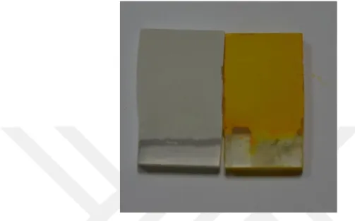
Figure 2.3. The ZnO structure (left) and CdS layer synthesized on ZnO structure (right) ... 43
Figure 2.4. (a) the left structure of ZnO/CdS/CdSe and the right ZnO/Cd, (b) CdSe synthesis solution... 44
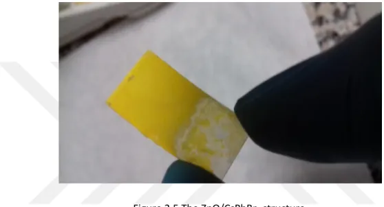
Figure 2.5. The ZnO/CsPbBr3 structure ... 45
Figure 2.6. The schematic of experimental PEC process. The left device is the AM1.5 light Source……….46
Figure 2.7. The absorption spectrum of the synthesized structures ... 48
Figure 2.8. The PL spectrum of the synthesized structures ... 48
Figure 2.9. The absorption spectrum related to the CsPbBr3 perovskite ... 49
Figure 2.10. The PL spectrum related to the CsPbBr3 perovskite ... 49
Figure 2.11. The schematic related to a photoelectron emitting due to an incident ... 50
Figure 2.12. (a) the ZnO structure XPS survey spectrum, (b) Zn 2p, and (c) O 1s ... 52
Figure 2.13. (a) the ZnO/CdS structure XPS survey spectrum, (b) Cd 3d, and (c) O2p ... 53
Figure 2.14. (a) the ZnO/CdSe structure XPS survey spectrum, (b) Se 3d ... 54
Figure 2.15. The ZnO/CdS/CdSe structure XPS survey spectrum ... 55
Figure 2.16. The XRD patters of structures ... 56
Figure 2.17. The SEM images of ZnO nanostructures with scale bars of (a) 100 µm, (b)20 µm, (c) 5 µm, and (d) 2 µm ... 57
Figure 2.18. The nanostructured ZnO under SEM with scale bars of (a)100 µm, (b)20 µm, (c) 5 µm ... 58 Figure 2.19. The SEM images of ZnO/CdSe nanostructures with scale bars of (a) 100 µm, (b)
xx
20 µm, (c) 5 µm, and 2 µm ... 59
Figure 2.20. The SEM images of ZnO/CdS nanostructures with scale bars of (a) 100 µm, (b) 20 µm, (c) 5 µm, and 2 µm ... 60
Figure 2.21. The SEM images of ZnO/CdS/CdSe nanostructures with scale bars of 100 µm… ... 61
Figure 2.22. The SEM images of ZnO/CsPbBr3 nanostructures with scale bars of 100 µm .. 62
Figure 2.23. The TEM images of ZnO structures with scale bar of (a) 100 nm, (b) 50 nm, (c) 20 nm, (d) 10 nm, (e)5 nm, and (f)5 nm ... 63
Figure 2.24. The TEM images of ZnO/CdSe structures with scale bar of (a) 100 nm, (b) 50 nm, (c) 20 nm, (d) 10 nm, (e) 5 nm, and (f) 5 nm ... 63
Figure 2.25. The TEM images of ZnO/CdS structures with scale bar of (a) 50 nm, (b) 10 nm, (c) 5 nm ... 64
Figure 3.1. The J-V curves of photoanode structures ... 69
Figure 3.2. The APBE performance of untreated structures ... 70
Figure 3.3. The stability of the photoanode structures ... 71
Figure 3.4. The responsivity of the structures ... 72
Figure 3.5. The IPCE of untreated structures ... 73
Figure 3.6. The J-V curve of the treated ZnO/CdSe structure ... 73
Figure 3.7. The J-V curve of the treated ZnO/CdS/CdSe structure ... 74
Figure 3.8. The APBE performances of treated structures ... 74
Figure 3.9. The IPCE of the treated structures ... 75
Figure 3.10. The IPCE of the ZnO/CsPbBr3 structure ... 75
xxi LIST OF TABLES
Page
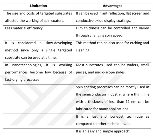
Table 2.1. Advantages and Limitation of Spin Coating Synthesis Method ... 41
Table 2.2. The elemental EDX of ZnO ... 42
Table 2.3. Elemental EDX of ZnO/CdS ... 43
Table 2.4. Elemental EDX of ZnO/CdSe ... 44
xxiii
LIST OF ABBREVIATIONS
CBD : Chemical Bath Deposition ALD : Atomic Layer Deposition CVD : Chemical Vapor Deposition ZnO : Zinc Oxide
MOCVD : Metal Organic Chemical Vapor Deposition PVD : Physical Vapor Deposition
LEDs : Light Emitting Diodes PVs : Photovoltaics
SEM : Scanning Electron Microscopy PL : Photoluminescence
IR : Infrared
ITO : Indium Tin Oxide
FTO : Fluorine Doped Tin Oxide FETS : Field Effect Transistors PEC : Photoelectrochemical CdS : Cadmium Sulfide CdSe : Cadmium Selenide CdTe : Cadmium Telluride QDs : Quantum Dots
HRTEM : High Resolution Transmission Electron Microscopy CsPbBr3 : Cesium Lead Bromide
PLQY : Photoluminescence Quantum Yield GaAs : Gallium Arsenide
VB : Valence Band CB : Conduction Band EDX : Energy Dispersive X-ray
XPS : X-Ray Photoelectron Spectroscopy XRD : X-Ray Diffraction
STH : Solar-to-Hydrogen
IPCE : Incident Photon-to-Current Conversion Efficiency ABPE : Applied Bias-to-Photon Efficient
xxv LIST OF SYMBOLS
Symbols Explanations Elocal Electric Field
β Field Enhanced Factor Φ Work Function Cox Gate Capacitance
h Planck Constant Ek Delocalized Energy
EB Electron Binding Energy
E0
ref Electrode Potential
Eref Working Electrode Potential
ERHE Working Electrode Potential Against the Electrolyte
Plight Sun Light Energy Flux
λ Light Wavelength
Iph Generated Photocurrent Density
VAg/AgCl Applied Voltage
E0
1
1. INTRODUCTION
1.1. Technology of Thin Film
Generation of electricity by controlling sunlight energy has been illustrated one of the solutions to the energy problems on a global scale. However, in order to compete with conventional sources, the solar device must be cost-effective and reliable. Various solar technologies including thin film, organic, and wafer have been investigated to achieve high efficiency, cost-effectiveness, and reliability with huge success. For example, crystalline silicon has been scaled up from laboratory to commercial very successfully and becomes 90% of the global solar device market [1]. To be cost effective, energy conversion efficiency should be increased, while less material is using. Instead of wafer technology meeting high efficiency, a thin film can convince the minimum amount of material usage in solar devices as well. During the past decade, novel thin film solar device technologies such as organic and dye-sensitized, zinc oxide, most recently perovskite photovoltaics and so on have been increasing with respect to device efficiency and stability. All thin film technologies depicted efficiency rises which are similar to crystalline silicon during the last decay [2]. The crystalline silicon has not been attained any lead over the technology of thin film. By the combination of single cells into multi-junction cell devices, the damage effects of light-induced degradation on the cell can be decreased dramatically. Therefore, the p-i-n structures tolerate less from set difficulties, even if the defect densities are developed. Since, in the p-i-n structures, an electric field dominant in the i-type section layer is promoted, and the set is gradually enhanced. Multi-junction structures pose a high light-harvesting potential in the solar spectrum because the bandgap energies of the single components are adjustable. In addition, compare to traditional solar devices such as crystalline silicon solar devices, the operation mechanism of many thin film solar devices technologies is in function of complex physical principles, such as functional material interfaces, charge separation, photoinduced, and excitonic processes [3]. Thin film technology has potential applications in energy conversion, harvesting and storage, because of their high performance, effective cost, and manufacturability. Thin film electrodes can be utilized in a wide variety of fields, such as photovoltaics, supercapacitor devices, fuel cells, rechargeable metal ion batteries and so on
2
[4]. Thin film materials could be manufactured by different approaches including chemical bath deposition (CBD), electrochemical deposition, thermal evaporation, atomic layer deposition (ALD), chemical vapor deposition (CVD), molecular beam epitaxy (MBE), pulsed laser deposition (PLD) and so on. By harnessing thin film manufacturing techniques, thin film electrodes with favorable properties can be obtained and the electrodes employed toward enhancing the performance of devices via an understanding of the performance structure and property correlations.
1.2. Zinc Oxide
Zinc oxide (ZnO) is a wide band gap semiconductor (3.3 eV). It has a higher exciton binding energy of 60 mV at room temperature with respect to other semiconductors. Its crystalline structure is wurtzite and it is a piezoelectric material and it has been studied in the form of single-crystal (bulk form) for decades [5]. Investigation in ZnO topics is still a controversial issue since there are unresolved issues concerning this material. ZnO nanostructure can be synthesized in a range of different morphologies and by a variety of methods, therefore it is of intense interest on a global scale. The wide varieties synthesis methods include CBD [6], wet chemistry [7], hydrothermal [8], electrospinning [9], flux method [10], sputtering [11], PLD [12], MBE [13], metal-organic chemical vapor deposition (MOCVD) [14], physical vapor deposition (PVD) [15], and top-down method using etching technology [16]. Among these methods, chemical methods such as CBD and wet chemistry synthesis are significant for some reasons: first of all they are capable of easy scaling up, low cost, and less hazardous. This method is compatible with flexible and organic materials; the growth occurs at a relatively low temperature; it can be combined with silicon technology, and there is no need for metal catalysts [17]. In chemical methods, the morphology and properties of ZnO nanostructures can be effectively controlled [18]. The flux and PVD techniques usually require high temperatures and impurities and catalysts can easily incorporate into the ZnO framework. Therefore, these methods are less likely to use in integrating with organic materials for flexible electronics. However, while metal-organic chemical vapor deposition and molecular beam epitaxy can produce a highly crystalline quality ZnO nanostructure, it has disadvantages including expensive, limited choice of material, low productivity yield, and poor deposition uniformity. Therefore, they are less adopted. The sputtering PVD, and PLD methods have less reproducibility and controllability with respect to other methods. Because of the highly polar surface of the wurtzite ZnO crystalline structure, it can grew in different nanostructures morphologies [19] including nanoflower [20], nanowire [21], astray [22], nanorods [23], nanobowls [24], nanospring [25], nanorings [26], nanobelts [27], nanohelics
3
[28]. Figure 1.1 depicts various morphologies of ZnO nanostructures. ZnO has potential applications in electronics and optoelectronics industries including light-emitting diodes (LEDs), photovoltaics (PV), photodetectors, laser, transistors, a catalyst for photoelectrochemical hydrogen production, sensors, and active elements in sunscreens, and so on.
1.2.1. Growth methods
Nanostructured ZnO can be fabricated by different methods, from simple to vacuum-based, low temperature, and low-cost approaches. Due to high defect chemistry, several optical and electronic properties have been observed for different nanostructured ZnO. There are very few controversial issues on the growth of undoped nanostructured ZnO. Since, there is a relationship between native defect concentration, growth conditions and measured properties which are not often clear. There are several aspects of the fabrication, including the use of seeding layer, metal catalysts, and so on. There is an unresolved problem for the vapor-phase fabrication of nanostructured ZnO. Two of them are the lateral position control and the size of the nanostructured ZnO on the substrates. To pattern, the substrate with multiple nanorods, the lithography method can be employed. But, to control the position of single nanorods, the feature size is too large. Self-assembly also can be used to pattern the ZnO nanostructures which is a simple and fast approach. For example, ZnO nanorod has been fabricated successfully by a self-assembled layer of polystyrene spheres [30]. The second issue related to the fabrication of nanostructured ZnO is controlling the doping ZnO nanostructures. Additionally, nanostructures ZnO should be strictly banned from exposure to the ambient. To prevent artifact and erroneous results, the characterization should be implemented on freshly prepared samples because of the time-dependent properties. The ZnO is sensitive to exposure to ambient. Because the humidity of the ambient affects the crystallinity and fabrication of ZnO nanostructures. It is also sensitive to the exposure to light and dry oxygen gas because of the persistent photoconductivity.
1.2.2. Stability of ZnO:
To avoid instability of the film properties, it is necessary to passivate ZnO with layers, especially for the p-type ZnO. The storage time, light exposure, and ambient humidity should be considered when characterizing ZnO nanostructures.
4 1.2.3. Post growth treatment
The properties of ZnO can be improved by post-growth treatments including hydrothermal treatment and annealing in different environments at high temperatures. The optical properties of ZnO can significantly change with both treatments. The hydrothermal treatments which are an excellent to traditional annealing implemented at the same time for the same temperature. The promotion in nanostructure ZnO properties occurs because of the reaction between native defects and water during the treatment causing a very big improvement for the defect formation. Since ZnO is sensitive to water vapor it is necessary to carefully control the time of treatment and water vapor pressure for optimal results [31]. 1.2.4. Properties of ZnO
Because of the unique chemical and physical characterizations, the nanostructured ZnO has potential applications in different areas.
1.2.4.1. Electronic and optical properties
There are several debate problems related to the electronic and optical properties of nanostructured ZnO, the most important one is being p-type doping and green emission. There are some hypotheses, and different defects which can result in energy levels of the ZnO band gap for the defect emission bands in ZnO band gap. There are two significant problems related to the electronic properties of nanostructure ZnO of p-type doping and n-type conductivity. To explain n-n-type conductivity and a shallow donor, while oxygen vacancy utilized to be considered as a possible candidate, it has been established that they are deep donors. In the ZnO, hydrogen is the most important shallow donor and it is also a factor for defected passivation. The hydrogen action as a shallow donor has been predicted and confirmed theoretically and experimentally for the ZnO structures, respectively. Hydrogen in nanostructure ZnO can be participated as subsurface hydrogen and bulk hydrogen, which is less bond, and it forms a complex with defects. Additionally, the stability problems and the change of properties because of the ambient and light exposure are also a problem for nanostructures, which are less stable with respect to thin films because of the high surface area. The P-type ZnO layer demonstrated stable p-type for 1 year, but n-type for 24 h. These phenomena were depicted as band bending. As a result, for p-type conductivity the presence of passivation layer for ambient protection must be considered. The protection layer also promotes the substrate properties especially optical properties of nanostructured ZnO. The charge transport and electrical properties can make a benefit from passivation.
5
6 1.2.4.2. Catalytic properties
Due to the low fabrication cost and large band gap of ZnO, it is received large consideration specially for the mineralization and degradation of pollutants as a photocataalyst. The ZnO generates electron and hole pairs under UV illumination which can fabricate hydrogen by splitting of water molecules, reduce graphene oxide to graphene, and synthesize H2O2. Particularly, the organic environmental pollutants can be oxidized or decomposed by generated holes, including formaldehyde, methyl blue, methyl orange, and rhodamine 6G. due to the active defect sites including the surface oxygen vacancies, ZnO can be employed as a catalyst for the production of methanol from hydrogen and carbon monoxide, and as a supporting building for different metal catalysts including copper/ferrite composites, copper oxide, cobalt, and gold, for methanol steam reforming. The nanostructured ZnO can be a perfect photocatalyst because of the huge surface to volume ratio with respect to the bulk ZnO structures. Additionally, if the length of nanostructured ZnO becomes smaller than 50 nm, the redox potential increases, the effective bandgap of ZnO increases, and therefore the photogeneration holes and electrons have a higher oxidizing/reducing power. The Large band gap energy is the main reason for recombination of the generated holes and electrons, which can promote the charge transition between the pollutants and the catalyst. To prevent the recombination for the generated hole and electron pairs and enhancing charge separation efficiency, ZnO can be combined with other nanostructures including cadmium sulfate, tin oxide, with a heterostructure array. The main drawback of nanostructured ZnO as a photocatalyst is the stability. Since it is unstable in basic and acidic media, therefore the photocatalytic activity of ZnO decreases over time due to photo corrosion under UV illumination.
1.2.4.3. Hydrophobicity of the ZnO
The surface wetting is one of the most significant factors for industry applications. There is a relationship between superhydrophobicity and superhydrophilicity of nanostructured ZnO structures by storage in dark and UV irradiation [31]. Figure 1.2 depicts a droplet on the nanostructured ZnO before and after UV illumination. By putting ZnO thin film in dark condition for seven days the superhydrophobicity can be restored. The process has been repeated for several times without any deterioration as depicted in figure 1.2b. This is related to the nano-porous surface photosensitivity of the ZnO structures. The wettability is controlled by the geometrical structure of the surface and also the material surface chemistry. A nanostructured ZnO structure subjects mostly to the non-polar low energy side
7
surface and is a rather porous structure, which perfectly promotes the hydrophobicity behavior. In particular, nanostructured ZnO generates hole and electron pairs under UV irradiation, and the holes can release the oxygen molecules with negatively charged absorbed on the nanostructured ZnO surface, which are ful by hydroxyl group, that therefore enhances the hydrophilicity phenomenon of the nanostructure surface.
Figure 1.2 (a) a spherical water droplet on nanostructure ZnO thin film after (right) and before (left) UV irradiation. (b) Reversible superhydrophobic superhydrophilic under UV irradiation and dark storage [31].
In the dark condition, the oxygen molecules replaced gradually the hydroxyl compounds on the nanostructured ZnO surface since their absorption is more favorable thermodynamically. Therefore, the hydrophobicity phenomenon can be restored.
1.2.4.4. ZnO field emission characterization
This property has applications in microwave devices, x-ray source, and photoelectric panel display. Due to high partial pressure of the oxygen during ZnO process, it has been become one of the best candidates as a field emission cathode. Having vertically aligned fine tips and relatively high density are desirable for the improved tips by local electric field. The nanotip
8
ZnO arrays (figure 1.3a) were fabricated via hydrothermal method on a ZnO seeding layer, with a ratio of 1:2 zinc source to HMTA [32]. Field emission investigated at room temperature in vacuum condition. The nanotip ZnO structures were positioned as a counter anode with certain size, and cold cathode, then the counter anode was placed away from the cathode at a known distance. By applying a voltage, an electric field built up between electrodes. To generate a certain current density, the threshold and the turn-on field were defined as the macroscopic required fields.
Figure 1.3. (a) synthesized ZnO nanoarrays. (b) Field emission current density versus electric field of ZnO nanotip arrays on Si substrate and (c) the corresponding plot [32].
Figure 1.3 (b) depicts a plot of field emission current density with respect to the applied field. Modification of the ZnO nanotips with metal nanoparticles reduced the turn-on field
9
effectively. One of the big advantages of nanostructured ZnO based field emission technology is the stability. Fowler-Nordheim (F-N) is governed the field emission behavior:
J =(AE2β2/Φ)exp(–BΦ3/2/βE), (1.1)
Where E is the macroscopic applied electric field (V/cm), term β is field enhanced factor, explained by
𝐸𝑙𝑜𝑐𝑎𝑙= 𝛽𝐸 = 𝛽𝑉
𝑑 (1.2)
Where Elocal is electric field of the emitter β tips, it is influenced by emitter density, vertical
alignment, crystal structure quality, and the emitter geometry. Having high β values is desirable. The density of emitters plays a significant role. Φ refers to work function for ZnO it is approximately 5.4 eV. B and A are two constants with values of 6.83 × 10³ (V·eV-3/2·m-1)
and 1.56 × 10¹⁰ (A·V-2·eV) respectively. And J is the current density emission in A/cm2. Figure
1.3 (c) depicts plotting of ln (J/E2) with respect to 1/ E, the curve demonstrates more than one
slope, due to absorbate induced emission saturation or the variation in the tip field.
1.2.4.5. Photonic crystals
The photonic crystal is defined when photons traveling inside the aligned structure, resulting in a contrast refractive index. In particular, when the nanostructured ZnO arrays are aligned vertically gives rise for photons transportation, it is called photonic crystal ZnO. When atom arrays in crystals give the electrical potential to an ordered distribution for inside electrons transportation, the result is an electronic band gap. Therefore, the crystal poses a band gap which is called ‘photonic band gap’. The defects can introduce the localized states in the photonic band gap in a photonic crystal, which is allowing the photons to diffusion at the localized states with specified frequencies. The photonic crystals properties control the diffusion and emission of photons in an optical communication system. In filtrating the empty sites between the nanostructured ZnO especially nanowires with a polymer and eliminating the nanowires with bases or acids can make reversed photonic crystals. The acceptable crystalline structure for being a photonic crystal is significant, since defects including grain, and voids can scatter the electromagnetic waves which are leading to loss by diffusion. Figure 1.4 depicts a transmission spectrum for a photonic crystal. High FWHM of the peak demonstrates a non-perfect photonic crystal.
10
Figure 1.4 The transmission spectrum of the ZnO nanowire arrays for both TE and TM polarizations [33].
1.2.4.6. Photoluminescence (PL) of ZnO
The photoluminescence of nanostructured ZnO, can be excited at room temperature by a UV light, with two emission bands. One in the visible region, comes from deep level recombination of the hole-electron caused by the surface and defects, for instance, the adhesion of the hydroxyl compounds in the crystal fabrication, zinc interstitials, and oxygen vacancies. The another is associated with the UV region peak, which arises due to emission from the band edge within exciton-exciton accident processes. Figure 1.5 (a) depicts a typical photoluminescence spectrum of nanostructured ZnO. There is a weak visible peak at around 500 nm, with dominant UV emission at near 380 nm. The emission in near infrared (IR) region at 760 nm for the nanostructured zinc oxide fabricated on the Au coated indium tin oxide (ITO) surface is associated with the second ordered characterization of UV emission [34]. The first peak blue-shift emission is because of the size of the nanostructured ZnO reduced to below 10 nm. The green emission derived from defect results in a reduction in quantum efficiency and exciton lifetime of the systems. To promote the band-edge UV emission and decrease emission from the defects, annealing in different atmospheres and different temperatures as post-plasma enhancement has been performed. The defect concentration can be reduced by annealing the structure at 200 °C. The defect and near-band-edge emissions can be effectively enhanced by coating a polymer on the nanostructure ZnO. Figure 1.5 (b) depicts a PL spectrum of nanostructured zinc oxide at 4.2 K. When the temperature reduced from 300 K to 4.2 K, the intensity of PL spectrum increased dramatically. The blue-shift from 378 nm to 368 nm is due to the shallow bound exciton. Since the band gap of semiconductors increase as the temperature reduces. Additionally, the
11
transversal and longitudinal optical (TO and LO) phonon replicas were also clear. As depicted in figure 1.5b, the separation of the energy between the mentioned phonon replicas is matched well phonon energies in nanostructured ZnO crystals.
Figure 1.5 (a) PL spectrum of nanostructure ZnO fabricated on the Au-coated surface. (b) PL spectrum of thin film ZnO and nanostructure ZnO at 4.2 K [34].
1.2.5. Applications of nanostructured ZnO 1.2.5.1. Electrochromic displays
The electrochromic display systems undergo color change on extraction driven or charged injection by applied voltage. They have four strategies including low power consumption and low cost, memory effects under open-circuit states, and high coloration efficiency. In
12
research, an electrochromic system has been demonstrated based on nanostructure ZnO [35]. The structure of the system has been demonstrated in figure 1.6. The wet chemical approach used to synthesize ZnO arrays on a transparent conductive material. Then methyl viologen molecules which are an organic chromophore were loaded onto the nanostructure. The molecules which were absorbed physically or chemically on the surface of the nanostructured ZnO stayed there with the aim of charge transport between viologen molecule and nanoarrays. The nanostructure provided charge transport path directly because the switching speed of the system was very fast. The viologen molecules reduced under a reverse bias, and become blue within approximately 170 ms, by removing the bias the color held for about 1 hour.
Figure 1.6 (a) The electrochromic system. (b) images of the system (i) before (ii) and after applying bias, (iii) circuit state [35].
1.2.5.2. ZnO structure in field-effect transistors
Field-effect transistors (FETs) based on nanostructured zinc oxide thin film has used in transparent and flexible electronics. Fabrication of ZnO in situ between drain and source electrodes is suitable with low-temperature wet chemical methods. Figure 1.7 depicts nanostructure ZnO transistor fabricated on polymer surface via an all- solution method [36]. The drain and source electrodes were manufactured Au nanoparticles followed by annealing. The ZnO nanomaterials have seeded the fabrication of nanostructure ZnO, and applied to the Au electrodes. As depicted in the figure. 1.7b, the nanostructure ZnO fabricated and connected the two electrodes through forming a nanostructure complex network, which is
13
depending upon the channel size between the drain and source electrodes. The contact between ZnO and Au must be ohmic. The work function mismatch between ZnO and Au are 4.5 eV and 5.1 eV respectively. The interfacial defect state is determined the transport properties. Figure 1.7c depicts the averaged transconductance gm (maximum value about
100 nS) and output characteristics, which demonstrated a n-type channel with off/on the 104-105 current ration.
According to:
µe =gm2L/2IdCoxW (1.3)
the electrons mobility µe in the nanostructured ZnO was measured to be 0.2 cm2/V·s. Where W and L are the channel width and length, Cox is the gate capacitance. The reduction in mobility of the electron in nanostructured ZnO was induced using the nanostructure process of the surface scattering. The transistor based on the nanostructure ZnO did not demonstrate a full saturated regime as the voltage of the drain was achieved, probably due to the impurity-derived grain boundaries and the dominant phonon scattering in the bridged nanostructure ZnO. The characterizations of the FETs strongly depend upon the nanostructured ZnO alignment.
1.2.5.3. Sensors
Based on the multijunctional p-n diode, the barrier height change, piezoresistance or resistance change of the nanostructure, the nanostructured ZnO used as an active component in the strain sensors, biosensors, UV visible-blind sensors, visible light sensors, and gas sensors. The ZnO can be functionalized with hydroxyl (OH-) or protons (H
3O+) groups with potential by changing the pH with respect to isoelectric point ZnO, since it is an amphoteric. The PH sensors can be utilized by nanostructure ZnO as an electrochemical probe. Since nanostructured ZnO arrays offer real-time detection, and high sensitivity. In a research, a very sharp nanostructured ZnO was fabricated on electrodes. The principal mechanism represented that any change in pH of the environment leads to change in potential of the nanostructure surface, then can be detected with any change in voltage between electrodes. Figure 1.8 depicts the potential between the reference and working electrodes which was proportional to buffer pH, with a perfect sensitivity of 52 mV/pH. The
14
Figure 1.7 (a) nanostructured ZnO transistor structure on a flexible substrate. (b) the nanostructure ZnO under SEM fabricated between the drain and source electrodes. (c) The output properties of nanostructure ZnO transistor with 10 µm channel. The inset depicts the transconductance with respect to the gate voltage [36].
nanostructured ZnO was thermodynamically stable at room temperature over the tested pH range. Therefore, to measure the intracellular pH value, the working and reference electrodes were pushed to enter to a human fat cell membrane. As demonstrated in figure 1.8b, the electrodes were in touch with cytoplasm of the cell, and analyzed the pH of the intracellular to be 6.8 [37]. To measure the pH in single living cell, this method is one of the
15
perfect ways. Since ZnO is biocompatible, nontoxic, and the intracellular measurement cannot affect the cellular viability.
Figure 1.8 (a) calibration plot for working and reference electrodes in a standard buffer. (b) The pH of the intracellular measurement inside a human fat cell [37].
1.2.5.4. Solar cells applications of ZnO
Traditional silicon solar cells have high carrier mobilities and low defect densities, and due to well-developed industrial fabrication technologies and the relatively high energy conversion efficiency, they are dominated by the solar energy industry. Different organic and inorganic compounds have been studied with the purpose of increasing efficiency by further decreasing cost of the energy per unit performance. The nanostructured ZnO is one of the best candidates for solar cell applications. Since it has fast electron transport and can be used as an electron transport layer (ETL) along the crystalline structures, high charge collection efficiency, very high area to volume ratio that can enhance the interfacial charge separation, and a very low reflectivity that can improve the absorption of light. The nanostructured ZnO have been carried out for excitonic and traditional p-n junction photovoltaics including
16
organic dye and inorganic nanoparticle sensitized organic and hybrid organic-inorganic solar cells.
1.2.5.5. Hydrogen generation via water splitting
Hydrogen gas is one of the important energy sources with a very high energy density quantity. Hydrogen reacts with oxygen to generate water and electricity without producing any by-products as pollutants. The nanostructured ZnO as a metal oxide semiconductor has potential as high-performance photocathodes or photoanode for splitting of the water molecules into a photoelectrochemical systems (PEC). Since, it has high electron mobility efficiency, low series resistance, flat band potential and suitable direct bandgap, and high surface to volume ratio. To promote absorption efficiency in the visible region, nanostructure ZnO can be combined with different semiconductors including CdSe, CdTe and CdS quantum dots, and ZnO-CdS core shell structures. Among the cadmium chalcogenides, the CdTe is more effective than others due to favorable band energy which can be injected the electrons into ZnO structure more than others. The quantum dots (QDs) can perfectly increase the efficiency by following multiple excitons from several layers of absorbed photon. The mott-Schottky analysis demonstrated a very suitable depletion thickness, flat band potential, and electron density. In the illumination condition, hole and electron pairs fabricate in the nanostructured ZnO then they separate in the depletion area at the nanostructured surface. Finally, the separated holes are injecting to the electrolyte and nanostructure interface to give rise to O2 by oxidizing and OH_the groups, while electrons are reducing the H+ groups and
producing H2, by flowing to the cathode.
Water molecule Splitting reaction is:
2 H2O + light 2 H2 + O2
Under +0.5 V external potential, the nitrogen doped nanostructure ZnO demonstrated a photon-to-hydrogen conversion of 0.15%. To promote the efficiency, nanostructure ZnO/multi-walled carbon nanotubes heterostructure were utilized to enhance the PEC device whole active surface area. The non-ideal and effective factors for the PEC system are including the dissolution and decomposition of the anode structure, that can be oxidized if the potential is more than the anode redox potential. The most second factor is the electrode surface energy of the states that can be non-homogeneous from the interior of the electrode. If the surface state levels are suitable, they can be used as electron transfer efficient channels. A piezoelectric potential can be carried out to drive different reactions for
17
water splitting [38]. Figure 1.9 depicts the working principles. The piezoelectric materials or nanostructures ZnO generate surface charge and undergo physical deformation on the compressive and tensile side under mechanical agitation by ultrasonic wave. Water molecules can be split into O2 and H2 in the molar ratio 1:2 when the applied piezopotential
is higher than the water standard redox potential (1.23 eV). This shows that the nanostructured piezoelectric materials can get wasted mechanical energy from the environment including vibrations noise, to fabricate hydrogen gas for green energy applications.
Figure 1.9 The diagram shows the charge and the ultrasonic vibration of the piezo potential created on a nanostructure ZnO [38].
1.3. Cadmium Chalcogenide Nanostructures
The nanostructured cadmium chalcogenides are carried out because of their significant optoelectronic and size-dependent physical and chemical properties. Recently, they have received attention. For example, nanostructured cadmium telluride (CdTe), cadmium selenide (CdSe), and cadmium sulfide (CdS) have been attained as an effective semiconductor for modern industrial applications. These nanoscale materials can be
18
fabricated with a variety of approaches for adjusting their properties with the aim of using in different applications including biosensor, biological fluorescence labels, light emitting diodes (LEDs), FETs, Photovoltaics (PVs), and so on. To enhance their properties, size and morphology harness of the nanostructures are main factors. Therefore, to control the size and morphology of the quantum dots (QDs), a variety of new synthesis method have been carried out.
1.3.1. Cadmium sulphide (CdS)
The CdS semiconductor (direct band gap of 2.42 eV) is a substance with significant chemical and physical properties, which made it a unique photocatalyst in different photochemical processes. CdS also has potential applications including infrared and laser detectors, gas sensors, nonlinear optical materials, optoelectronic and luminescence systems. It is also demonstrated excellent visible light detecting properties. To synthesis of CdS there are varieties of methods.
1.3.2. Cadmium selenide (CdSe)
The CdSe is a semiconductor with controllable size-dependent physical and chemical properties. They can be used in fabrication of LEDs, solar cells, luminescent biological labels, and so on. Interestingly, to harness the properties, the size of the nanostructures become important with respect to Exciton Bohr radius of bulk structure. By controlling the size of CdSe, the quantum confinement of photo-generated hole and electron pairs allow the tuning of optical properties of the nanostructures. In CdSe, the lowest unoccupied or conduction band has 5s orbitals of cadmium, whereas, the highest occupied or valence band has 4P orbitals of selenium.
1.3.3. Synthesis of chalcogenide nanostructures
There are several synthesis methods for nanostructure chalcogenides semiconductors including spray pyrolysis, synthesis from elemental powders, ionic liquid assisted synthesis, solid state reaction, hydrothermal/solvothermal process, pulse plasma assisted route, sonochemical, synthesis into micellar medium, γ-irradiation route, microwave assisted route, single source molecular precursor route, template/self-assembled - assisted synthesis, colloidal precursors, chemical bath deposition, and so on. Stabilized and uniformly dispersed
19
nanostructures are successfully implemented by using surfactants and capping agents. Functionalized nanostructures with biomolecules and polymers have been fabricated for biological functionalities and optoelectronic. By investigating the effect of process parameters including the use of cosurfactants, the role of surfactants and solvents, temperature, molar ratios, and concentration of ion source precursor, the reaction conditions have been enhanced in different fabrication methods. The formation mechanism of nanostructures has been clarified for several approaches. Different researches focused on the physical and chemical properties related to specific applications including photocatalysts, luminescence for lasing and optoelectronics, so on. Cadmium chalcogenide nanostructures have a potential application such as gas sensing, pollutant reducers, photocatalysts, LEDs, solar cells, and so on. Advances in the fabrication methods have been attained in synthesis nanomaterials or/and nanostructures with varying morphologies. To get the desired shape and size, the basic idea has been processed with a harnessed reaction to start arrested and nucleation growth. However, each route has its limitations and advantages. Therefore, the synthesis of controlled and functionalized nanostructures still poses a great challenge.
1.3.3.1. Colloidal synthesis method
One common method for the fabrication of nanostructure semiconductors is harnessing the precipitation by a suspension of colloidal nanoparticles. The method idea arises from the slowly injection of the metal ions solution into the non-polar or polar solution of chalcogenide ion source precursor. By adjusting the size of nanostructure after the nucleation step, the fabrication is stopped immediately by harnessing the equilibrium between the solvated ions and the nanocrystals of desired chalcogenides. Most investigations have been carried out for controlling and identifying the effective factors that influence such equilibrium. The factors are including the concentration and molar ratio of the precursors, the role of the solvents, and the temperature which have been found very significant. To achieve very stable and monodispersed nanostructure quantum dots, surfactants, polymers, and other molecules can be used as coated agents. For example, it has been reported that the chalcogenide capped with thiol are very stable. Figure 1.10 depicts the schematic diagram for the fabrication of CdTe nanostructure quantum dots functionalized with thiol ligand [39]. Thioacetamide, thiourea, H2S, and Na2S can be used as the sulfur source. The drawbacks of the methods are including invariably related surface defects and large size distribution, and poor crystallinity of nanostructures.
20
Figure 1.10. Schematic depicts the fabrication of thiol capped CdTe quantum dots. Left depicts the formation of CdTe precursor by H2Te gas. Right depicts growth of CdTe QDs by reflux [39].
1.3.3.2. High temperature injection
For the fabrication of cadmium chalcogenide nanostructures, single molecule decomposition of the precursors prepares effective and convenient routes. In this synthesis route, molecular complex including the chalcogen and cadmium metal are thermally decomposed in a non-polar coordinating solvent. The fabrication of core-shell-shell CdS/CdSe/CdTe nanostructure QDs reported using the precursor of materials dispersed in an organometallic reagent such as tri-octylphosphile (TOP) is followed by the organometallic pyrolysis on injection into a coordinating solvent, tri-northophosphine oxide (TOPO) [40] at a very high temperature as depicted in the diagram figure 1.11. The formation of the nanostructures QDs initiated by the precursors decomposition whereas the fabrication of nanostructures is prevented when the precursor supply is unloaded. The size control synthesis of nanostructure QDs carries out in three steps: 1) The injection of precursors, 2) the nucleation, 3) the Ostwald ripening growth control of the nuclei. The resulted QDs can be agglomerated as TOPO passivated. The QDs nanocrystals provided by this approach have more crystalline quality than those fabricated by colloidal methods.
21
Figure 1.11. Representation of hot injection approach in organo-metallic fabrication of QDs nanostructures [40].
To provide a single-source precursor from available chemicals, many scientists used simple cadmium salts instead of selenocarbamates and dithiocarbamates of metal compounds of dithiobiurea as a single-source precursor for the synthesis of high-quality and mono dispersed QDs with adjustable color tuning. The limitations prohibited using such approaches including the toxic materials such as CE2 (E=Se or S) for the fabrication of the materials precursor. Cadmium thiolate, metal chalcogenolates and selenolate derivatives were used as precursors for fabrication of nanostructured cadmium selenide and sulfide. Monodispersed cadmium chalcogenide nanostructures (CdE; E=Te, Se, S) can be fabricated by organometallic materials including formaldehyde. Cadmium chalcogenide nanostructures were also synthesized by using tributylphosphine (TBP) at high temperatures. In an environment-friendly approach cadmium oxide, carbonate, and acetate were used as a greener cadmium source instead of dimethyl cadmium. The nanostructured Zn, Cu, Pb, Mn, Hg, and Cd sulfide can be fabricated by thermal decomposition. However, because of the fact that, using pyrophoric and highly toxic materials as metal sources, and alkyl amines, TOPO as a solvent which have high boiling point, requires special inert gas and high temperature environment that makes the approach complex for scaling up and more expensive.
1.3.3.3. Hydrothermal/Solvothermal process
The hydrothermal process carried out under temperature and pressure reaction between the different precursors; the approach is called the hydrothermal process. This approach utilizes high boiling point solvent through autogenously high temperature and high pressure in an autoclave. Therefore, it is very suitable for fabricating highly crystalline nanostructures
22
by using cheap low boiling solvents. The water can be used as an environmental solvent. Recently, wide variety numbers of precursors have been used to fabricate metal chalcogenide nanostructures via hydrothermal method. The effective factors for morphology and the size of nanostructures are 1) temperature, 2) the time of hydrothermal decomposition, 3) the type of surfactants used, and iv) the nature of the solvent used. The hydrothermal method has benefits including purity of nanophase, the nanostructures size distribution, but morphology difference still remains and needs to overcome.
1.3.3.4. Microwave-Assisted synthesis
In this approach, microwave radiation induces a chemical reaction to produce desired products. The electromagnetic field with high-frequency radiations force on the charged particle solution and generating molecular rotation or charge migration. This process may generate further polarization in polar molecules. Micron size structures with different morphologies can be fabricated by using visible light and simple aqueous method under microwave and employing different Sulphur ion source. The nanostructured CdS can also fabricate using thiourea and cadmium acetate in certain solvent via microwave irradiation. The molar ratio of precursors has been found also critical. This method has advantages including purity of materials, small particle size, short reaction time.
1.3.3.5. Sonochemical process
In this method, the energy is transferred to the solution by an ultrasonic radiation. The ultrasonic radiation interacts with the molecules and solution and the energy improves the reaction activating. The synthesis with the sonication method is a significant approach for the fabrication of nanostructures. The ultralysis is based on cavitational heating by collapsing bubbles and surface damage and emulsification. The ultrasonic wave forms bubbles in solution that collapse each other; this process is defined as cavitation process. During bubble formation, heat transfer to the solution and an extreme situation is generated, this phenomenon induces the chemical reaction.The nanostructured CdSe, CdS, and other chalcogenides can be synthesized using the sonochemical method. The nanostructures with different morphologies including nanowires or nanotubes, nanorods can be fabricated using sonochemistry by using direct growth helping agents. Sonochemically synthesis has potential advantages including small particle size, better thermal stability, and uniform size distribution.
23 1.3.3.6. Capping-Assisted synthesis
To develop diversified QDs semiconductors, capping synthesis is very promising since the morphology of the crystals is strongly dependent upon the type of capping lignad attracted on their surface. The surfactants play a significant role in the fabrication of nanostructures especially in controlling morphology, shape, and size of the fabricated nanostructures as well as stabilization to specific assemblies. These assembly methods are including bilayer liquid membranes, Langmuir Blodgett film, micro-emulsion, monolayers, micelle, reverse micelle, and so on. Nanostructured cadmium, zinc, and lead chalcogenides have been fabricated using surfactant assemblies. Thiol coated nanostructures QDs are water-soluble since thiol capping agents are hydrophilic molecules that are strongly coordinated to the QDs and a polar group such as amine, carboxyl, and hydroxide ensuring hydrophobicity. They can be also coated with a polymer and biologically active macromolecules. The macromolecules including polymer, RNA, DNA, proteins, and amino acids can control the growth and nucleation of QDs. Some advantages have been brought by biological macromolecules conjugation including biocompatibility and bioactivity, and biological functionality which can provide on the surface of QDs. This has brought many applications including bio-labeling, drug delivery by luminescence probing, and so on.
1.3.4. Applications of metal chalcogenide nanostructures
Quantum dots or chalcogenide nanoparticles have potential applications in medical technology to material science. They demonstrated continuous absorption spectra, long term photostability, tunable quantum efficiency, and narrow emission, therefore they are invariable materials for different photovoltaic and biomedical applications. Their applications include Optoelectronic materials for LEDs, photo-catalyst, degradation of pollutants, reduction of dyes and pigments, photochemical applications, photo-catalysis, solar cells (both QDs organic-inorganic and sensitized hybrid), and so on. Among the biomedical applications, cancer therapy, drug delivery, DNA labeling and observation of diagnosis have attracted more attention. Recently, the QDs have been used in long term in vivo and in vitro cell trafficking, and high-resolution cellular imaging, tumor targeting, drug delivery and diagnostics [41]. Figure 1.12 depicts the classification of potential biomedical applications of QDs in bio-imaging and bio-sensing.
24
Figure 1.12. The classification of biomedical applications of QDs [41]. .
The possibility of utilizing QDs semiconductors as fluorescence labeling reagents for biological imaging experiments has been depicted by a core-shell structure such as CdSe/ZnS and CdSe/CdS attached to proteins and DNA molecules. Because of the unique emission properties of QDs, a lot of color probes can be distinguished in a single exposure and excited by a single narrowband excitation source. This can make QDs superior to use organic chromophores. The QDs have been demonstrated as the best systems for intracellular investigations including tracking single molecules in the cell, investigation of the dynamic cellular processes, and visualizing the cellular structure. However, metal chalcogenide bare QDs possess toxicity and have a hydrophobic surface, therefore, they cannot be used in vivo without surface modification and functionalization. By suitable surface modification, it has been possible to reduce toxicity and increase hydrophilicity.
1.4. Halide Perovskites
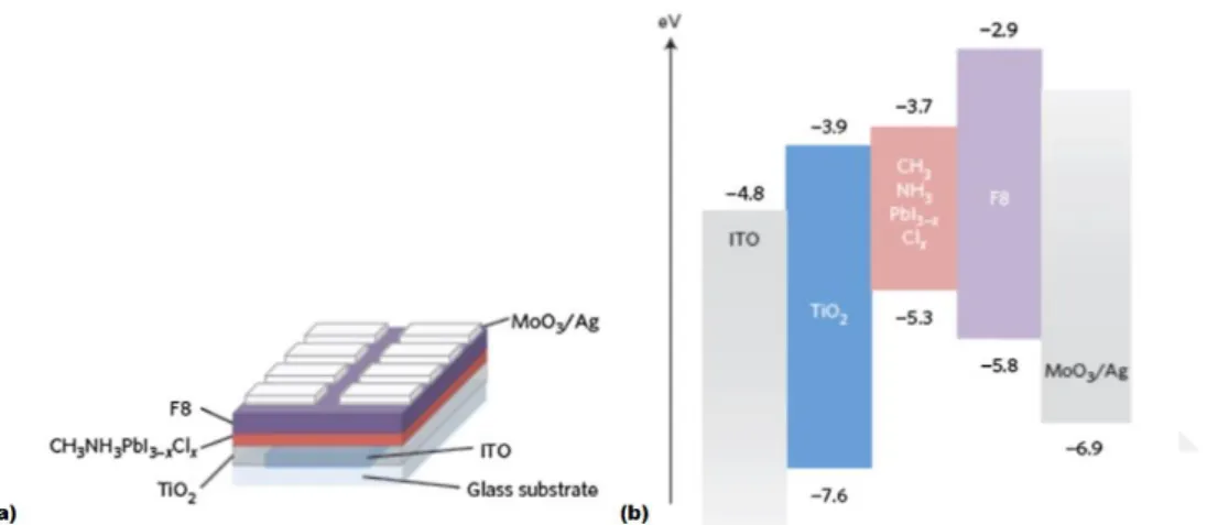
The nanostructured perovskites have been attracted high attention in optoelectronic industries due to their unique electronic and optical properties such as cost-effective and easy solution processability, bandgap tenability over the visible region, sharp absorption edge with small urbech tails, and long charge carrier propagation. Their electronic and optical properties can be varied in different visible ranges by the composition differences of metal ion (Ge2+, Pb2+, Sn2+), cation formamidinium or methylammonium as well as an anion (Br-, I-, Cl-), which form a 3D structure of the AMX
3 type as demonstrated in figure 1.13 a. Additionally, the shape, size, morphology and dimension of nanostructured perovskites can be adjusted with a variation ratio between perovskite precursor and the amine chain ligands (figure 1.13). Due to strong anisotropy and quantum confinement, they show size- shape-dependent electronic and optical properties distinct from their bulk structure peers. QDs based on Perovskite suppose a dimension in size smaller than the exciton Bohr radius. In
![Figure 1.4 The transmission spectrum of the ZnO nanowire arrays for both TE and TM polarizations [33]](https://thumb-eu.123doks.com/thumbv2/9libnet/3751435.28087/36.892.170.619.130.348/figure-transmission-spectrum-zno-nanowire-arrays-te-polarizations.webp)
![Figure 1.9 The diagram shows the charge and the ultrasonic vibration of the piezo potential created on a nanostructure ZnO [38]](https://thumb-eu.123doks.com/thumbv2/9libnet/3751435.28087/43.892.157.694.370.829/figure-diagram-charge-ultrasonic-vibration-potential-created-nanostructure.webp)
![Figure 1.11. Representation of hot injection approach in organo-metallic fabrication of QDs nanostructures [40]](https://thumb-eu.123doks.com/thumbv2/9libnet/3751435.28087/47.892.181.796.117.402/figure-representation-injection-approach-organo-metallic-fabrication-nanostructures.webp)

![Figure 2.1 CBD synthesis of nanostructured layers, with the system components [50].](https://thumb-eu.123doks.com/thumbv2/9libnet/3751435.28087/66.892.298.540.110.346/figure-cbd-synthesis-nanostructured-layers-components.webp)