IOP Conference Series: Materials Science and Engineering
PAPER • OPEN ACCESS
Band Structure and Optical Properties of Kesterite
Type Compounds: first principle calculations
To cite this article: S Palaz et al 2017 IOP Conf. Ser.: Mater. Sci. Eng. 175 012014
View the article online for updates and enhancements.
Related content
Prediction of semiconducting behavior in minority spin of Co2CrZ (Z = Ga, Ge, As): LSDA
D. P. Rai and R. K. Thapa
-First Principles Study of Half-metallic Properties at MnSb/GaSb(001) Interface
Elmira Sartipi, Alireza Hojabri, Arash Bouchani et al.
-Electronic structure and optical properties of rare earth hexaborides RB6 (R = La, Ce, Pr,Nd, Sm, Eu, Gd)
Nirpendra Singh, Sapan Mohan Saini, Tashi Nautiyal et al.
Band Structure and Optical Properties of Kesterite Type
Compounds: first principle calculations
S Palaz1, H Unver2, G Ugur3, A M Mamedov4,5*, E Ozbay4
1
Department of Physics, Harran University, Urfa, Turkey,
2
Department of Physics, Ankara University, Ankara, Turkey,
3
Department of Phisics, Gazi University, Ankara, Turkey
4
Nanotechnology Research Center-NANOTAM, Bilkent University, Ankara, 06800 Turkey,
5
International Scientific Research Center, Baku State University, Baku, AZ-1148, Azerbaijan
E-mail: [email protected]
Abstract. In present work, our research is mainly focused on the electronic structures, optical and magnetic properties of Cu2FeSnZ4 ( Z = S, Se) compounds by using ab initio calculations within the generalized gradient approximation (GGA). The calculations are performed by using the Vienna ab-initio simulation package (VASP) based on the density functional theory.The band structure of the Cu2FeSnZ4 ( Z = S, Se) compounds for majority spin (spin-up) and minority spin (spin-down) were calculated . It is seen that for these compounds, the majority spin states cross the Fermi level and thus have the metallic character, while the minority spin states open the band gaps around the Fermi level and thus have the narrow-band semiconducting nature. For better understanding of the electronic states, the total and partial density of states were calculated, too. The real and imaginary parts of dielectric functions and hence the optical functions such as energy-loss function, the effective number of valance electrons and the effective optical dielectric constant for Cu2FeSnZ4 ( Z = S, Se) compounds were also calculated.
Keyword: ab initio calculation; elastic constant; electronic structure; quaternary semiconductors
1. Introduction
Along the progress of growing high-quality complex compounds, the group I2-II-IV-VI4 quaternary
semiconductors have rapidly been broad interest due to many possibilities in varying the chemical composition, and thereby optimizing the material functionality. Especially cupper based kesterite materials (Cu2XYZ4, X=Zn, Fe, Y=Sn, Ge, Z=S, Se, Te) have recently found increased interest as
absorber layer in thin film solar cells technologies and devices [1]. The band gap energy of Cu2XYZ4are suitable for photovoltaics, and Cu2XYZ4 have the advantage over corresponding
CuIn(Ga)Se2 absorbers to involve abundant, nontoxic, and less expensive chemical elements.
Cu2XYZ4 compounds have experimentally and theoretically [2-5] been verified to crystallize in either
S4 2
kesterite or D2d 11
stannite structure although disordered structure also has been reported [6]. Cu2ZnSnS4 based solar cells have recently achieved solar energy conversion efficiency of 12.6%.
While Cu2ZnSnS4 itself has many attractive properties for solar cells, further increases in the
ICCMPT IOP Publishing IOP Conf. Series: Materials Science and Engineering 175 (2017) 012014 doi:10.1088/1757-899X/175/1/012014
International Conference on Recent Trends in Physics 2016 (ICRTP2016) IOP Publishing
performance will require optimisation that can be achieved through control of the materials stoichiometry and/or incorporation of extrinsic impurities, such as Fe (to replace Zn) or Se (to replace S) [7]. In particular, Fe is of interest for Si-based tandem solar cells since the lattice constant of Si lies between two end members of the alloy, Cu2ZnSnS4 and Cu2FeSnSe4, and an increase in the band gap
could also be beneficial.
Further analysis of the material properties as well as future transport simulations of various device structures require a detailed understanding of the electronic conducting-band and valence-band structures.
In the present work, by means of DFT (Density Functional Theory) approach we examined the series of Cu2FeSnS4 (CFTS), and Cu2FeSnSe4 (CFTSe) assuming they crystallize in the typical S4
2
and D2d 11
structures. For these compounds we derived structural, mechanical, optical properties. Consequently, the primary purpose of this work is to provide some additional information to the existing data on the physical properties of CFTS and CFTSe compounds by using the ab-initio total energy calculations.
2. Calculation methodology
The first principles calculation based on DFT was used with the aid of the VASP [8-10] program. The exchange and correlation potentials were Perdew-Burke-Ernzerhof method [11] based on generalized gradient approximation (GGA). The plane wave cut-off energy in the wave vector K space was 500 eV. We have performed the Brillouin–Zone integration by using 9x9x9 gamma centered special Monkhorst-Pack k-points [12]. When the total energy was stabilized within 1×10⁻⁷ eV, the force acting on each atom of the cell after optimization was less than 0.001 eV/Å, the residual stresses of the cell was less than 0.001 GPa, and the tolerance offset was less than 1×10⁻⁵
Å.
The elastic constants are calculated by the efficient stress-strain method [13] as implemented in the VASP code. The optical properties were obtained complex dielectric function ε(ω)=ε1(ω)+iε2(ω)
where the details explained in Refs. [14].
3. Results and Discussion
3.1 Mechanical Properties
The estimated independent elastic constants are tabulated in Table 1. To our knowledge, there are no experimental or theoretical data available for elastic constants. The calculated elastic constants satisfy Born criteria [15]. Therefore, it can be said that, CFTS and CFTSe compounds for considered structures are mechanically stable.
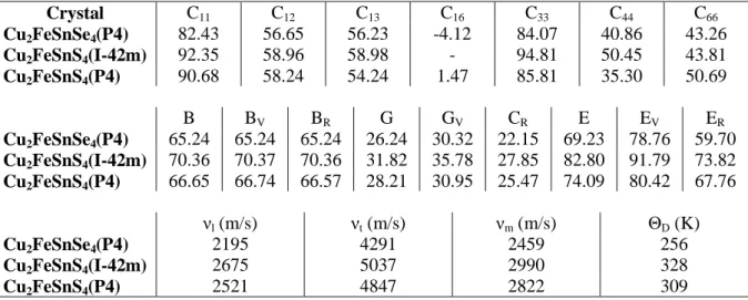
Table 1. The calculated elastic constants (Cij, in GPa) , isotropic bulk modulus (B, in GPa), shear
modulus (G, in GPa) and Young’s modulus (E, in GPa), the longitudinal, transverse and average elastic wave velocities together with the Debye temperature for Cu2FeSnZ4 ( Z = S, Se) compounds
Crystal C11 C12 C13 C16 C33 C44 C66 Cu2FeSnSe4(P4) 82.43 56.65 56.23 -4.12 84.07 40.86 43.26 Cu2FeSnS4(I-42m) 92.35 58.96 58.98 - 94.81 50.45 43.81 Cu2FeSnS4(P4) 90.68 58.24 54.24 1.47 85.81 35.30 50.69 B BV BR G GV CR E EV ER Cu2FeSnSe4(P4) 65.24 65.24 65.24 26.24 30.32 22.15 69.23 78.76 59.70 Cu2FeSnS4(I-42m) 70.36 70.37 70.36 31.82 35.78 27.85 82.80 91.79 73.82 Cu2FeSnS4(P4) 66.65 66.74 66.57 28.21 30.95 25.47 74.09 80.42 67.76 νl (m/s) νt (m/s) νm (m/s) ΘD (K) Cu2FeSnSe4(P4) 2195 4291 2459 256 Cu2FeSnS4(I-42m) 2675 5037 2990 328 Cu2FeSnS4(P4) 2521 4847 2822 309 2
ICCMPT IOP Publishing IOP Conf. Series: Materials Science and Engineering 175 (2017) 012014 doi:10.1088/1757-899X/175/1/012014
The isotropic bulk moduli (Bv), shear moduli (G), Young’s moduli (E), Poisson’s ratios, B/G ratios,
elastic constants (Cij) Debye temperatures, and sound velocities are calculated by using Voigt
Reuss-Hill [16-18] approach. The results are tabulated in Table 1. It shows that the compressibility of these structures is relatively same after application of pressure. We note that the B/G values are all higher than 1.75. Therefore, the studied systems in its all forms can be classified as ductile materials. Our calculated values of Poisson’s ratio vary from 0.31 to 0.40 for these structures. Thus indicating strong semi-metalic contribution in the intra-atomic bonding for these structures.
3.2 Electronic structure
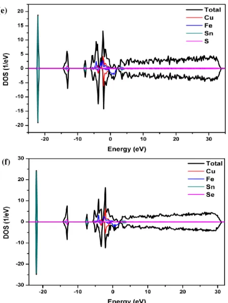
The electronic structure plays an important role in determining of the properties of the Kesterite compounds. By using the equilibrium lattice constants the calculated band structure dispersion in k-space along high symmetry direction in the Brillouin zone, the total and partial density of states are presented in Figs. 1-3. The band structure of the CFTS and CFTSe compounds were calculated for majority spin (spin-up) and minority spin (spin-down). It is seen that for these compounds, the majority spin states cross the Fermi level and thus have the metallic and semimetallic characters, while the minority spin states open the band gaps around the Fermi level and thus have the narrow-band semiconducting nature. For these crystals the unit cell contains four atoms. In order to understand the contribution of each orbital in these atoms we also investigate the angular momentum decomposition of the atoms projected density of states (DOS). DOS show that all these orbitals are spatially delocalized. Energy fragment from -7 eV till Fermi level originated from more localized Cu (d), and delocalized Se or S(s,p), Sn(p) states with small contribution from Sn(s,d), Fe(s,p), Se or S(d), and Cu(s,p) states. Finally, the structure from conduction band minimum and above presents an admixture of Cu (s,p), Sn (p,d), Fe(s,p), Se (s,p,d) and S(p) states. One can see a strong hybridization between Cu(p), Fe(d) and Sn(d) states and also some overlap between Se or S(s) and Sn(s) states, at around -14 eV.
(a)
ICCMPT IOP Publishing IOP Conf. Series: Materials Science and Engineering 175 (2017) 012014 doi:10.1088/1757-899X/175/1/012014
(b)
(c)
(d)
4
ICCMPT IOP Publishing IOP Conf. Series: Materials Science and Engineering 175 (2017) 012014 doi:10.1088/1757-899X/175/1/012014
Figure 1. The calculated electronic band structure and DOS of compounds. The electronic band
structure for (a) Cu2FeSnS4(I42M), (b) Cu2FeSnS4(P4) and (b) Cu2FeSnSe4(P4). DOS for (d)
Cu2FeSnS4(I42M), (e) Cu2FeSnS4(P4) and (f) Cu2FeSnSe4(P4).
3.3 Optical properties
We have first calculated the real and imaginary part of ε(ω)=ε1 (ω)+iε2 (ω) complex dielectric function
using the Kramers-Kroning relations. The optical constant such as energy-loss function, the effective number of valance electrons and the effective optical dielectric constant have been calculated with the help of the real and imaginary part of dielectric function for these compounds. The results obtained show manner similar to our recent works [19]. The energy values of ε1x (ε1z) that decreasing
(dε1)/(dE<0) and increasing (dε1)/(dE>0)are zero are 7.04 eV and 16.63eV for CFTSe compound, 7.46
eV and 17.64 eV for CFTS compound. These values that the ε1x (ε1z) are zero are points reduced of
the reflections, and show that the polarization disappears. The maximum peak values of ε2x (ε2z) are
0.66 eV, 4.73 eV, and 7.21 eV for CFTS compound, 0.60 eV, 4.45 eV, and 6.54 eV for CFTSe compound. These values show how much the electromagnetic wave polarizes the system, and corresponds to the electronic transitions from the valance band to the conduction band. Furthermore, energy region above 8 eV for CFTS and CFTSe compounds, respectively is the region where dispersion and transparency are low. This energy region corresponds to the region beginning of the transition between the bands. The 1.4-8.0 eV energy region for these compounds is the region where
(e)
(f)
ICCMPT IOP Publishing IOP Conf. Series: Materials Science and Engineering 175 (2017) 012014 doi:10.1088/1757-899X/175/1/012014
the transitions between the bands are very intense. The 1.6-8.0 eV energy region has reduced transitions between the bands. The energy region above 10 eV also corresponds to the collective vibration of valance electrons. This energy region defined as plasma oscillations is described by the energy loss function (L). The sharp maxima in the energy-loss function are associated with the existence of plasma oscillations. The optical data for CFTS and CFTSe show that in the limit of IR or visible region of the spectrum that have been studied the values of the real part of the dielectric constant lie near zero. This means that the negative contribution from the accelerating mechanism of absorption is quite small and is compensated by the positive contribution from the real and virtual interband transitions of electrons. Such a behavior of the ε1function indicates the low concentration of conduction electrons in Cu2FeSnZ4. The presence of a Drude component in the dielectric functions of
Cu2FeSnZ4 (D2d11 phase) permitted us to determine the parameters of free electrons – plasma
frequency of conduction electrons Epl = 19.2 eV and the effective number of free electrons - Neff =
2.4x1022 cm-3. The low values of Neff indicate the formation of a pseudogap in the energy band
spectrum of Cu2FeSnZ4. In the case of Cu2FeSnZ4, the zero values of ε1 prevent making corresponding
estimates for Neff. However, it is reasonable to explain the observed behavior of the dielectric properties of Cu2FeSnZ4 by the formation of a deeper pseudogap in the density of states. Our results
concerning the low-energy interband absorption indicate a weak “growing-in” of the gap in the density of states, which was predicted theoretically for the both phases of Cu2FeSnZ4.
4. Conclusions
In this work, we have investigated mechanical, electronic, and optical properties of CFTS and CFTSe compounds. The results of elastic constants reveal all compounds are mechanically stable. The traditional B/G ratio indicate that considered compounds possess ductile nature. The electronic structure calculations show that the majority spin states cross the Fermi level and thus have the metallic character, while the minority spin states open the band gaps around the Fermi level and thus have the narrow-band semiconducting nature. Finally, optical properties were studied and discussed.
References
[1] Jimbo K, Kimura R, Kamimura T, Yamada S, Maw W S, Araki H, Oishi K and Katagiri H 2007Thin Solid Films.515 5997
[2] Katagiri H, Saitoh K, Washio T, Shinohara H, Kurumadani T and Miyajima S 2001 Sol. Energy Mater. Sol. Cells.65 141
[3] Moriya K, Watabe J, Tanaka K and Uchiki H 2006Phys. Status Solidi C. 32848
[4] Babu G S, Kumar Y B K, Bhaskar P U, and Raja V S 2008Semicond. Sci.Technol.23 085023 [5] Chen S, Gong X G, Walsh A and Wei S H 2009 Appl. Phys. Lett.94041903
[6] Schorr S 2007 Thin Solid Films.515 5985 [7] Persson C2010 J. Appl. Phys.107053710
[8] Kresse G and Furthmuller J 1996 Comp. Mater. Sci.6 15 [9] Blochl P E 1994 Phys. Rev. B.50 17953
[10] Kresse G andFurthmuller J 1996 Phys. Rev. B.54 11169
[11] Perdew J P, Burke K, and Ernzerhof M 1996 Phys. Rev. Lett .77 3865 [12] Monkhorst H J and Pack J D 1976 Phys. Rev. B.13 5188
[13] Kocak B, Ciftci Y O, Colakoglu K, Deligozand E, and Tatar A 2013 Materials Science and Technology29 925
[14] Simsek S, Koc H, Palaz S,Oltulu O, Mamedov A M and Ozbay E 2015 Ferroelectrics.483 26 [15] Born M 1940 Proc. Cambridge Philos. Soc.36 160
[16] Voight W 1928Lehrbook der kristall physic Leipsig: Teubner [17] Reuss A and Angew Z 1929 Math Mech9 49
[18] Hill R 1952 Proc. Phys. Soc. London7065349
[19] Koc H, Simsek S, Palaz S,Oltulu O, Mamedov A M and Ozbay E 2015 Phys. Stat.Sol. (c). 12(6) 651
6
ICCMPT IOP Publishing IOP Conf. Series: Materials Science and Engineering 175 (2017) 012014 doi:10.1088/1757-899X/175/1/012014