Abstract—InGaN/GaN light-emitting diodes (LEDs) make an
important class of optoelectronic devices, increasingly used in
lighting and displays. Conventional InGaN/GaN LEDs of
c-ori-entation exhibit strong internal polarization fields and suffer
from significantly reduced radiative recombination rates. A
reduced polarization within the device can improve the optical
matrix element, thereby enhancing the optical output power and
efficiency. Here, we have demonstrated computationally that
the step-doping in the quantum barriers is effective in reducing
the polarization-induced fields and lowering the energy barrier
for hole transport. Also, we have proven experimentally that
such InGaN/GaN LEDs with Si step-doped quantum barriers
indeed outperform LEDs with wholly Si-doped barriers and those
without doped barriers in terms of output power and external
quantum efficiency. The consistency of our numerical simulation
and experimental results indicate the effects of Si step-doping in
suppressing quantum-confined stark effect and enhancing the hole
injection, and is promising in improving the InGaN/GaN LED
performance.
Index Terms—InGaN, GaN, light-emitting diode (LED),
quantum-confined Stark effect (QCSE), Si-doping.
I. I
NTRODUCTIONT
ARGETTING for general lighting, a significant progress
in InGaN/GaN light-emitting diodes (LEDs) has been
made since the first InGaN/GaN-based LED was demonstrated
[1]. Typically, a high external quantum efficiency (EQE) is
Manuscript received May 24, 2012; revised May 30, 2012; accepted May 31, 2012. Date of publication July 18, 2012; date of current version March 15, 2013. This work is supported by the Singapore National Research Foundation under Grant NRF-RF-2009-09 and Grant NRF-CRP-6-2010-2, and by the Singapore Agency for Science, Technology and Research (A*STAR) SERC under Grant 112 120 2009.
Z.-H. Zhang, S. T. Tan, Z. G. Ju, W. Liu, Y. Ji, and Z. Kyaw are with
LUMI-NOUS! Center of Excellence for Semiconductor Lighting and Displays, School
of Electrical and Electronic Engineering, Nanyang Technological University, 639798 Singapore (e-mail: [email protected]; [email protected]; [email protected]; [email protected] [email protected]; zinm0013@ntu. edu.sg).
Y. Dikme is with AIXaTech GmbH, 52074 Aachen, Germany (e-mail: [email protected]).
X. W. Sun is with LUMINOUS! Center of Excellence for Semicon-ductor Lighting and Displays, School of Electrical and Electronic Engi-neering, Nanyang Technological University, 639798 Singapore (e-mail: [email protected]).
H. V. Demir is with LUMINOUS! Center of Excellence for Semiconductor Lighting and Displays, School of Electrical and Electronic Engineering, School of Physical and Mathematical Sciences, Nanyang Technological University, 639798 Singapore, and also with the Department of Electrical and Electronics Engineering, Department of Physics, UNAM—Institute of Materials Science and Nanotechnology, Bilkent University, Bilkent, Ankara 06800 Turkey (e-mail: [email protected]).
Color versions of one or more of the figures are available online at http:// ieeexplore.ieee.org.
Digital Object Identifier 10.1109/JDT.2012.2204858
observed from InGaN/GaN LEDs under low current injection
levels. However, the efficiency is substantially reduced under
elevated current injection, and yet high current is required
in most of the lighting applications [2]. This effect is well
recognized as the efficiency droop. Various models have thus
far been proposed to explain the droop, such as junction heating
[3], electron overflow [4], [5], reduced effective radiative
recombination rate due to the elevated plasma temperature
caused by carrier-carrier and carrier-photon collisions [5],
current crowding [6] and Auger recombination [7].
To date, several methods have been suggested to improve the
efficiency and enhance the optical output power. For example,
Lee et al. enhanced the efficiency by grading InN fraction in
InGaN quantum well structures [8]. Wang et al. improved the
efficiency by incorporating quantum wells with graded
thick-ness [9]. Zhao et al. employed thin AlInN barriers to suppress
the thermionic carrier escape rate [10]. Additionally, electron
blocking layers (EBL) that improve the emission of InGaN/GaN
LEDs, including stepwise-stage EBL [11], p-type AlGaN/GaN
superlattice with a graded AlN composition [12], AlGaN EBL
with graded AlN fraction [13], and even AlInN EBL [14] has
also been studied. Recently, it has been shown that
three-dimen-sional hole gas [15] is effective in increasing the hole
concen-tration, thus enhancing the optical power.
Besides improving the carrier injection efficiency, it is
necessary to increase the electron-hole wave function overlap
. For that, staggered InGaN quantum wells have been
proposed and investigated [16]–[20]. The spatial separation
of the electron-hole wave functions can be reduced also by
employing either the ternary InGaN substrate [21] or the
electro-plated Ni metal substrate [22]. Recently, c-plane
III-Ni-tride quantum wells with embedded “delta” novel materials
have proved to be effective in enhancing the electron-hole wave
function overlap, therefore increasing the radiative
recombi-nation rates [23]–[26]. The strain induced spatial separation
of electron-hole wave functions can further be completely
eliminated in the non-polar quantum wells and increased
ra-diative recombination rates can thus be obtained [27], [28]. It
has also been shown that the material quality and the device
performance can be substantially improved by introducing
Si doping in quantum barriers [29]–[31]. However, Si-doped
barriers or even Si-delta-doped barriers usually have a setback
from holes blocking [32], [33], which leads to a high local hole
accumulation. Previously, Zhu et al. proposed the selective
Si doped barriers to symmetrize the hole distribution and
improve the LED performance [34]. Nevertheless, selective Si
doping could not effectively suppress the polarizations in those
quantum wells due to the undoped quantum barriers. On the
other hand, it has been reported that the free electrons (released
Fig. 2. (a) Experimentally measured and (b) numerically simulated optical output power and EQE as a function of current for Devices I, II, and III.
by Si-doped quantum barriers) could screen the quantum
confined Stark effect (QCSE), though the screening effect is
not optimum due to the absence of ionized dopants [35]. In
this work, we study both numerically and experimentally on
the step-doping of the quantum barriers with Si, which could
effectively screen the QCSE through the ionized dopants by
properly designing the doped thickness and position in the
quantum barriers. This provides additional degree of freedom
of designing thicker quantum wells to avoid carrier high energy
state filling, relieving the efficiency droop in c-plane LEDs
[36]. The proposed step-doped quantum barriers could reduce
hole blocking effect, promote electron injection, quench
polar-ization fields and enhance electron-hole wave function overlap
within the quantum wells. These improvements
trans-late to the enhancement of optical output power and efficiency.
II. E
XPERIMENTSTo investigate the proposed step-doped barriers, InGaN/GaN
LED epitaxial wafers were grown by AIXTRON
close-cou-pled showerhead metal–organic chemical-vapor deposition
(MOCVD) reactor on c-plane sapphire substrates [37]. The
growth was initiated on a 30 nm thick low-temperature grown
u-GaN buffer layer (at 560 C with a growth pressure of 600
mbar and a V/III ratio between NH and TMGa of 950). A
2
m thick u-GaN layer was subsequently grown at 1050
C with a growth pressure of 400 mbar and a V/III ratio of
2700. For the n-GaN growth (with
cm ),
the growth temperature, pressure and V/III ratio were set to
1060 C, 250 mbar and 1140, respectively. A higher V/III
ratio of 10064 was utilized for the growth of quantum
bar-riers. The growth temperature was 820 C and 737 C for the
quantum barriers and quantum wells, respectively, while the
V/III [NH3]/[TEGa] [TMIn]) ratio during the quantum well
growth was 10500. However, a constant growth pressure of
400 mbar was used during the growth of both the quantum
barriers and quantum wells. The LED samples were finally
covered with a 300 nm thick p-GaN grown at 950 C with the
pressure of 150 mbar, and the hole concentration of our p-GN is
1.0
10
cm . The structures were annealed in the ambient
of N for 15 min at 687 C. In our experiment, Cp Mg and
diluted SiH were used as p-type and n-type dopant sources,
respectively.
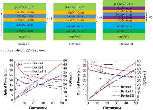
In our study, we comparatively studied three structures of
InGaN/GaN LED epi-wafers, which are called Devices I, II,
and III. The schematic diagrams of the investigated devices are
shown in Fig. 1. Among them, Device I is a standard LED with
undoped barriers, while Device II is designed with 12 nm thick
barriers each fully doped with Si (
cm ), and
Device III features step-doped barriers (6 nm undoped and
fol-lowed by 6 nm doped with
cm ). The three
devices differ only in their quantum barriers.
The studied LEDs all consist of 5-pair quantum well stack
(In
Ga
N/GaN with 3 nm well and 12 nm barrier) as the
active region. The devices were fabricated by using standard
fabrication process. The LED mesa was obtained through
reac-tive ion etch with a size of 300 m 300 m. Ni/Au (5 nm/150
nm) was deposited as the p-electrode, and then the thermal
an-nealing was performed for the p-electrode in the mixture of N
and O for 5 min. Finally Ti/Au (30 nm/150 nm) was deposited
on the n-GaN layer as the n-electrode.
III. R
ESULTS ANDD
ISCUSSIONFig. 2(a) shows the measured EQE and optical output
power as a function of the current for all the devices (along
with Fig. 2(b) depicting the numerical simulation results). As
demonstrated, Device II performs better than Device I when
the current is increased beyond 26.5 mA, as the Si-doped
barriers replenish electrons in the quantum wells. Furthermore,
the screening effect on the QCSE improves the spatial overlap
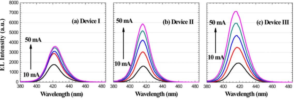
Fig. 3. EL spectra for: (a) Device I; (b) Device II; and (c) Device III.
Fig. 4. (a) Simulated hole concentration and (b) simulated radiative recombination rates for Devices I, II, and III at I mA.
between the electron and hole wave functions [29], thus
en-hancing the radiative recombination rates. Nevertheless, in
the low current regime (4.8 mA
mA), Device II
performs worse than Device I. On the other hand, across the
whole current range tested, we see that Device III outperforms
Devices I and II, and the power is experimentally enhanced
by 90.79% between Devices I and III, while 27.90% between
Devices I and III at 50 mA. Fig. 3 presents the
electrolumi-nescence (EL) for the studied devices, where the emission
intensity is the strongest for Device III and the weakest for
Device I. Meanwhile, Devices II and III show a shorter peak
emission wavelength compared to Device I, which is attributed
to the slightly relieved QCSE by Si-doped quantum barriers
[29]. However, the less pronounced blue-shift for all the three
devices as the injection current increases is caused by the
junction heating effect [38].
In order to better understand the improvement of EQE
and optical output power in Devices I, II and III, numerical
simulations were performed by APSYS [39], which
self-con-sistently solves the Poisson equation, continuity equation and
Schrödinger equation with proper boundary conditions. The
self-consistent six-band
theory is used to take account of the
effect of carrier screening in InGaN quantum wells [40]. Here,
the Auger recombination coefficients are taken to be 1
10
cm /s [7], [41]. The offset ratio between the conduction and
valence bands for InGaN/GaN quantum well is assumed to be
70:30 [42]. Also, a 40% of the theoretical polarization charge
is used due to the crystal relaxation through generating
disloca-tions [43]. The other parameters used in the simulation can be
found elsewhere [44]. Fig. 2(b) depicts the calculated EQE and
optical output power, which demonstrates that similar trends of
the enhanced EQE and optical output power are observed after
employing Si-doped quantum barriers in Device III compared
to Devices I and II. However, in the simulation, we did not
consider the localized states caused by potential fluctuation of
InGaN alloys [45], and the temperature/carrier concentration
dependence of those non-radiative recombination factors (e.g.,
Auger recombination, Shockley-Read-Hall recombination),
which caused the discrepancy between simulation and
experi-ment [refer to Fig. 2(a) and (b)].
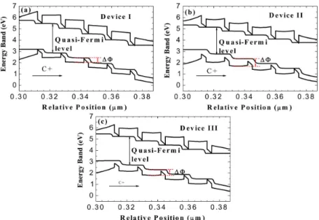
It is reported that the wholly-doped barrier increases the
bar-rier height for holes, thus retarding the hole injection [32], which
explains the worse performance of Device II compared to
De-vice I in low current regime (4.8 mA
I
mA).
Fortu-nately, hole-blocking effects in Device II can be suppressed by
employing step-doped barriers. It is observed from Fig. 2(a) and
(b) that Device III performs better than Device II due to an
im-proved hole transport.
To better probe the hole transport of Devices I, II, and III,
we simulated the hole distribution and radiative recombination
rates in their quantum wells [Fig. 4(a) and (b)]. As shown in
Fig. 4(a), all devices possess the highest hole concentration in
the fifth quantum well (the one closest to p-GaN) along
[0001]-orientation. However, due to the highest valence-band barrier
height in the wholly-doped Si barriers (Fig. 5 and Table I),
De-vice II cannot inject holes efficiently into the quantum wells that
are close to n-GaN side (e.g., the first quantum well). On the
other hand, Device III has half the thickness of doped barriers
compared to Device II, which reduces the overall valence-band
barrier height for the hole injection (Fig. 5 and Table I). As a
result, a much more homogeneous hole distribution can be
ob-tained in Device III, which correspondingly leads to higher
ra-diative recombination rates in the quantum wells close to the
n-GaN side for Device III compared to Device II. Even though
Fig. 5. (a) Simulated energy band for (a) Device I, (b) Device II, and (c) Device III. represents the energy barrier height for holes. TABLE I
ENERGYBARRIERHEIGHT FOREACHQUANTUMBARRIER INDEVICESI, II,ANDIII. QUANTUMBARRIER1 REFERS TO THEBARRIERAFTER THEFIRST QUANTUMWELLWHILEQUANTUMBARRIER5 REFERS TO THEBARRIERAFTER THEFIFTHQUANTUMWELL
Device I shows the most homogeneous hole distribution among
the three devices due to the smallest energy barrier height (Fig. 5
and Table I), it suffers from the strongest QCSE and hence the
low radiative recombination rates, as shown in Fig. 4(b).
As is well recognized, the strong polarization induced field
within the quantum wells spatially separates the electron and
hole wave functions, thus reducing the interband transition
probability of carriers. However, the internal electric field
profile can be tuned by Si-doping the quantum barriers. On
the other hand, it can be seen clearly from Fig. 4(b) that the
fifth quantum well dominates the radiative recombination rates
especially for Devices II and III. Thus analyzing the electric
field in the fifth quantum well for these three devices
compar-atively is helpful for us to understand the mechanism for the
QCSE suppression. Fig. 6(a) presents the electric field in the
fifth quantum well for Devices I, II, and III under equilibrium,
where the positive direction is along [0001]. We can see a
considerably flat electric field profile in Device I, whereas for
devices with Si-doped quantum barriers (Devices II and III),
the electric field is tilted as depicted in Fig. 6(a); a reduction
of the electric field in the well close to the n-GaN side [“B”
site in Fig. 6(a)] is achieved, while an enhanced magnitude of
electric field is simultaneously triggered at the interface close
to p-GaN side [“A” site in Fig. 6(a)]. Fig. 6(b)–(d) shows the
energy band diagrams and the charge profile for Devices I,
II, and III under equilibrium, respectively. In Device I, only
polarization induced charges are shown in Fig. 6(b), since there
are no Si dopants in the quantum barriers and the simulated
electron sheet charge density
in the fifth quantum well is
around 1.4
10 cm , which is negligible compared to the
polarization charge density that is in the order of 10
cm
[29]. Thus we obtain the macroscopic electric field in (1) at
both “A” and “B” sites, respectively, which explains the field
symmetry for Device I in Fig. 6(a)
(1)
where
is the elementary electronic charge,
is the relative
dielectric constant of InGaN,
is the it electric permittivity in
vacuum, and
is denoted as the polarization induced charge
density.
For Devices II and III, the Si dopants can be considered to
be completely ionized [46], feeding electrons into the quantum
well and leaving a depletion region in the barrier. The sheet
charge density of the ionized Si atoms can be obtained from
, where
is the Si dopant concentration (
cm
for both Devices II and III) and
is the doped
barrier thickness (
nm and 6 nm in for Devices II and III,
respectively), and therefore we obtain the sheet charge density
of Si
, which is
cm
and
cm
for Device II and III, respectively. Besides, according to our
simulation, the
in the fifth quantum well is about 3.0
10
cm
and 1.5
10
cm
in Devices II and III, respectively,
Fig. 6. (a) Simulated electric field profile in the fifth quantum well, where the positive direction is along the [0001], energy band diagram and charge profile for: (b) Device I; (c) Device II; (d) Device III; (e) combined conduction band diagrams; and (f) combined valance band diagrams for Devices I, II, and III. Data collected under equilibrium.
which are slightly smaller than
by our simple calculation
above. The smaller
compared to
is due to the loss of
electron leaking into p-GaN region. Since we do not observe any
holes diffusing into the quantum wells under the equilibrium
state in the simulations, the effect of holes is not included here.
Accordingly, the electric field at “A” site in Device II can
be given by (2) [refer to Fig. 6(c)], while it can be expressed
in (3) for Device III if the diffused
from the doped part in
the quantum barrier is negligible compared to
as shown in
Fig. 6(d). However, the electric field at “B” site for both Devices
II and III can be represented in (4) according to Fig. 6(c) and (d)
(2)
(3)
(4)
where
and
represent the electric field caused by Si
dopants and electrons, respectively.
It is well-known that the idea to screen the QCSE by
intro-ducing Si dopants in the quantum barriers is realized by
re-leasing electrons [33] into the quantum wells [i.e.,
in (2)
and (3)], but, the effect of the ionized donors has never been
properly recognized. As shown in (4), a reduced electric field at
“B” site [Fig. 6(a)] caused by the presence of ionized Si dopants
[Fig. 6(c) and (d)] helps to make the valence band less titled for
Devices II and III compared to Device I (Fig. 6(f),
meV for Device II and 50 meV for Device III), which in turn
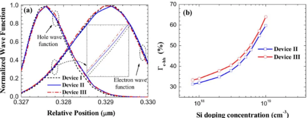
pushes the hole wave function towards “A” site [Fig. 7(a)].
Thus, Device II and III enjoy a more overlapped electron-hole
wave function than Device I. Device I has a
of 29.94%,
while Device II and Device III feature a
of 34.81% and
37.76%, respectively. The smallest
is responsible for the
weakest emission intensity for Device I [Fig. 3(a)]. Moreover,
the more increased
in Device III compared to Device II
is attributed to the reduced electric field at “A” site compared
to Device II, as a reduced field at “A” site that is caused by the
absence of ionized Si dopants [refer to (2) and (3)] tilts the
con-duction band more (Fig. 6(e),
meV for Device II and
50 meV for Device III) and pushes the electron wave function
towards “B” site more [Fig. 7(a)]. Therefore, the largest
translates to the strongest emission intensity for Device III as
shown in Fig. 3(c). Moreover, according to our simulation,
vice III shows even better screening effect to QCSE than
De-vice II, and thus ideally a shorter wavelength is expected for
Device III. However, as shown in Fig. 3(b) and (c), the peak
emission wavelengths for Devices II and III are very close, the
difference is ranged from 1.9 to 0.4 nm for various currents we
used. As the devices were grown in different runs by MOCVD,
it is possible, for example, we may have some slight difference
in Indium incorporation in the quantum wells. The peak
wave-length difference between Device II and III is a combined result
generated from different QCSE screening effect and possibly
Indium incorporation. Nevertheless, in order to verify the effect
of step-doping feature, we have further investigated
for
Devices II and III as a function of Si doping concentration in
their quantum barriers as shown in Fig. 7(b), which indicates
the advantage of the step-doped architecture in Device III over
the wholly doped barriers in Device II.
IV. C
ONCLUSIONIn conclusion, the effect of Si step-doped quantum barriers
on the optical power and EQE of InGaN/GaN LEDs is studied.
Fig. 7. (a) Normalized electron and hole wave functions for Devices I, II, and III at 50 mA, and (b) for Devices II and III as a function of Si-doping concentration at 50 mA.
Improvements have been observed in the proposed LED device
with Si step-doped quantum barriers. This is mainly attributed
to the reduced barrier height for the hole injection and the
ex-cellent screening effect on QCSE. Furthermore, LEDs with Si
step-doped quantum barriers shows better screening effect on
the QCSE than LEDs with Si fully doped quantum barriers.
The proposed approach of step-doped quantum barriers can be
used to increase the efficiency and hence holds great promise
for high-efficiency GaN-based LEDs.
A
CKNOWLEDGMENTThe authors would like to thank Dr. K. L. Ke and Dr. C. B.
Soh for their assistance in electroluminescence measurement
in IMRE (Institute of Materials Research and Engineering) of
A*STAR (Agency for Science, Technology and Research).
R
EFERENCES[1] S. Nakamura, M. Senoh, and T. Mukai, “P-GaN/N-InGaN/N-GaN double-heterostructure blue-light-emitting diodes,” Jpn. J. Appl.Phys.
Pt. 2-Lett., vol. 32, pp. L8–L11, Jan. 1993.
[2] S. T. Tan, X. W. Sun, H. V. Demir, and S. P. DenBaars, “Advances in the LED materials and architectures for energy-saving solid-state lighting toward ‘lighting revolution’,” IEEE Photon. J., vol. 4, no. 2, pp. 613–619, Apr. 2012.
[3] A. A. Efremov, N. I. Bochkareva, R. I. Gorbunov, D. A. Lavrinovich, Y. T. Rebane, D. V. Tarkhin, and Y. G. Shreter, “Effect of the Joule heating on the quantum efficiency and choice of thermal conditions for high-power blue InGaN/GaN LEDs,” Semiconductors, vol. 40, pp. 605–610, May 2006.
[4] M. H. Kim, M. F. Schubert, Q. Dai, J. K. Kim, E. F. Schubert, J. Piprek, and Y. Park, “Origin of efficiency droop in GaN-based light-emitting diodes,” Appl. Phys. Lett., vol. 91, pp. 183507-1–183507-3, Oct. 2007. [5] W. Chow, M. H. Crawford, J. Y. Tsao, and M. Kneissl, “Internal ef-ficiency of InGaN light-emitting diodes: Beyond a quasiequilibrium model,” Appl. Phys. Lett., vol. 97, pp. 121105-1–121105-3, Sep. 2010. [6] H. Y. Ryu and J. I. Shim, “Effect of current spreading on the effi-ciency droop of InGaN light-emitting diodes,” Opt. Express, vol. 19, pp. 2886–2894, Feb. 2011.
[7] Y. C. Shen, G. O. Mueller, S. Watanabe, N. F. Gardner, A. Munkholm, and M. R. Krames, “Auger recombination in InGaN measured by pho-toluminescence,” Appl. Phys. Lett., vol. 91, pp. 141101-1–141101-3, Oct. 2007.
[8] Y. J. Lee, C. H. Chen, and C. J. Lee, “Reduction in the efficiency-droop effect of InGaN green light-emitting diodes using gradual quantum wells,” IEEE Photon. Technol. Lett., vol. 22, no. 10, pp. 1506–1508, Oct. 2010.
[9] C. H. Wang, S. P. Chang, W. T. Chang, J. C. Li, Y. S. Lu, Z. Y. Li, H. C. Yang, H. C. Kuo, T. C. Lu, and S. C. Wang, “Efficiency droop allevia-tion in InGaN/GaN light-emitting diodes by graded-thickness multiple quantum wells,” Appl. Phys. Lett., vol. 97, pp. 181101-1–181101-3, Nov. 2010.
[10] H. P. Zhao, G. Y. Liu, R. A. Arif, and N. Tansu, “Current injection effi-ciency induced effieffi-ciency-droop in InGaN quantum well light-emitting diodes,” Solid-State Electron., vol. 54, pp. 1119–1124, Oct. 2010. [11] S. J. Huang, Y. K. Su, C. Y. Tseng, S. C. Lin, and H. C. Hsu,
“Im-provement of light intensity for nitride-based multi-quantum well light emitting diodes by stepwise-stage electron emitting layer,” Appl. Phys.
Express, vol. 3, pp. 122106-1–122106-3, 2010.
[12] S. J. Lee, S. H. Han, C. Y. Cho, S. P. Lee, D. Y. Noh, H. W. Shim, Y. C. Kim, and S. J. Park, “Improvement of GaN-based light-emitting diodes using p-type AlGaN/GaN superlattices with a graded Al composition,”
J. Phys. D—Appl. Phys., vol. 44, p. 105101, Mar. 2011.
[13] Y. K. Kuo, J. Y. Chang, and M. C. Tsai, “Enhancement in hole-in-jection efficiency of blue InGaN light-emitting diodes from reduced polarization by some specific designs for the electron blocking layer,”
Opt. Lett., vol. 35, pp. 3285–3287, Oct. 2010.
[14] S. Choi, H. J. Kim, S. S. Kim, J. Liu, J. Kim, J. H. Ryou, R. D. Dupuis, A. M. Fischer, and F. A. Ponce, “Improvement of peak quantum effi-ciency and effieffi-ciency droop in III-nitride visible light-emitting diodes with an InAlN electron-blocking layer,” Appl. Phys. Lett., vol. 96, pp. 221105-1–221105-3, May 2010.
[15] J. Simon, V. Protasenko, C. X. Lian, H. L. Xing, and D. Jena, “Polar-ization-induced hole doping in wide-band-gap uniaxial semiconductor heterostructures,” Science, vol. 327, pp. 60–64, Jan. 2010.
[16] R. A. Arif, Y. K. Ee, and N. Tansu, “Polarization engineering via staggered InGaN quantum wells for radiative efficiency en-hancement of light emitting diodes,” Appl. Phys. Lett., vol. 91, pp. 091110-1–091110-3, Aug. 2007.
[17] R. A. Arif, H. P. Zhao, Y. K. Ee, and N. Tansu, “Spontaneous emission and characteristics of staggered InGaN quantum-well light-emitting diodes,” IEEE J. Quantum Electron., vol. 44, pp. 573–580, May–Jun. 2008.
[18] H. P. Zhao, G. Y. Liu, J. Zhang, J. D. Poplawsky, V. Dierolf, and N. Tansu, “Approaches for high internal quantum efficiency green InGaN light-emitting diodes with large overlap quantum wells,” Opt. Express, vol. 19, pp. A991–A1007, Jul. 2011.
[19] H. P. Zhao, G. Y. Liu, X. H. Li, G. S. Huang, J. D. Poplawsky, S. T. Penn, V. Dierolf, and N. Tansu, “Growths of staggered InGaN quantum wells light-emitting diodes emitting at 520–525 nm employing graded growth-temperature profile,” Appl. Phys. Lett., vol. 95, pp. 061104-1–061104-3, Aug. 2009.
[20] H. P. Zhao and N. Tansu, “Optical gain characteristics of staggered InGaN quantum wells lasers,” J. Appl. Phys., vol. 107, pp. 113110-1–113110-12, Jun. 2010.
[21] J. Zhang and N. Tansu, “Improvement in spontaneous emission rates for InGaN quantum wells on ternary InGaN substrate for light-emitting diodes,” J. Appl. Phys., vol. 110, pp. 113110-1–113110-5, Dec. 2011. [22] J. H. Son and J. L. Lee, “Strain engineering for the solution of efficiency
droop in InGaN/GaN light-emitting diodes,” Opt. Express, vol. 18, pp. 5466–5471, Mar. 2010.
[23] H. P. Zhao, R. A. Arif, and N. Tansu, “Self-consistent gain analysis of type-II ‘W’ InGaN-GaNAs quantum well lasers,” J. Appl. Phys., vol. 104, pp. 043104-1–043104-7, Aug. 2008.
[27] R. M. Farrell, P. S. Hsu, D. A. Haeger, K. Fujito, S. P. Denbaars, J. S. Speck, and S. Nakamura, “Low-threshold-current-density AlGaN-cladding-free m -plane InGaN/GaN laser diodes,” Appl. Phys. Lett., vol. 96, pp. 231113-1–231113-3, 2010.
[28] R. M. Farrell, D. A. Haeger, P. S. Hsu, K. Fujito, D. F. Feezell, S. P. Denbaars, J. S. Speck, and S. Nakamura, “Determination of internal pa-rameters for AlGaN-cladding-free m-plane InGaN/GaN laser diodes,”
Appl. Phys. Lett., vol. 99, pp. 171115-1–171115-3, 2011.
[29] L. W. Wu, S. J. Chang, T. C. Wen, Y. K. Su, J. F. Chen, W. C. Lai, C. H. Kuo, C. H. Chen, and J. K. Sheu, “Influence of Si-doping on the characteristics of InGaN-GaN multiple quantum-well blue light emit-ting diodes,” IEEE J. Quantum Electron., vol. 38, no. 5, pp. 446–450, May 2002.
[30] Z. Zheng, Z. Chen, Y. Xian, B. Fan, S. Huang, W. Jia, Z. Wu, G. Wang, and H. Jiang, “Enhanced electrostatic discharge properties of nitride-based light-emitting diodes with inserting Si-delta-doped layers,” Appl.
Phys. Lett., vol. 99, pp. 111109-1–111109-3, 2011.
[31] H. P. D. Schenk, A. Bavard, E. Frayssinet, X. Song, F. Cayrel, H. Ghouli, M. Lijadi, L. Naïm, M. Kennard, Y. Cordier, D. Rondi, and D. Alquier, “Delta-doping of epitaxial GaN layers on large diameter Si(111) substrates,” Appl. Phys. Express, vol. 5, pp. 025504-1–025504-3, 2012.
[32] J. H. Ryou, J. Limb, W. Lee, J. P. Liu, Z. Lochner, D. W. Yoo, and R. D. Dupuis, “Effect of silicon doping in the quantum-well barriers on the electrical and optical properties of visible green light-emitting diodes,” IEEE Photon. Technol. Lett., vol. 20, no. 11, pp. 1769–1771, Nov. 2008.
[33] M. K. Kwon, K. Park, S. H. Baek, J. Y. Kim, and S. J. Park, “Si delta doping in a GaN barrier layer of InGaN/GaN multiquantum well for an efficient ultraviolet light-emitting diode,” Journal of Appl. Phys., vol. 97, pp. 106109-1–106109-3, May 2005.
[34] D. Zhu, A. N. Noemaun, M. F. Schubert, J. Cho, E. F. Schubert, M. H. Crawford, and D. D. Koleske, “Enhanced electron capture and symmetrized carrier distribution in GaInN light-emitting diodes having tailored barrier doping,” Appl. Phys. Lett., vol. 96, pp. 121110-1–121110-3, Mar. 2010.
[35] V. Fiorentini, F. Bernardini, F. Della Sala, A. Di Carlo, and P. Lugli, “Effects of macroscopic polarization in III–V nitride multiple quantum wells,” Phys. Rev. B, vol. 60, pp. 8849–8858, Sep. 1999.
[36] L. Wang, C. M. Lu, J. N. Lu, L. Liu, N. Y. Liu, Y. J. Chen, Y. F. Zhang, E. D. Gu, and X. D. Hu, “Influence of carrier screening and band filling effects on efficiency droop of InGaN light emitting diodes,”
Opt. Express, vol. 19, pp. 14182–14187, July 2011.
[37] Z. G. Ju, S. T. Tan, Z.-H. Zhang, Y. Ji, Z. Kyaw, Y. Dikme, X. W. Sun, and H. V. Demir, “On the origin of the redshift in the emission wavelength of InGaN/GaN blue light emitting diodes grown with a higher temperature interlayer,” Appl. Phys. Lett., vol. 100, pp. 123503-1–123503-3, 2012.
[38] Z. Gong, S. Jin, Y. Chen, J. McKendry, D. Massoubre, I. M. Watson, E. Gu, and M. D. Dawson, “Size-dependent light output, spectral shift, and self-heating of 400 nm InGaN light-emitting diodes,” J. Appl.
Phys., vol. 107, pp. 013103-1–013103-6, 2010.
[39] APSYS by Crosslight Software Inc., Burnaby, Canada, [Online]. Avail-able: http://www.crosslight.com
[40] H. Zhao, R. A. Arif, Y. K. Ee, and N. Tansu, “Self-cnsistent analysis of strain-compensated InGaN-AlGaN quantum wells for lasers and light-emitting diodes,” IEEE J. Quantum Electron., vol. 45, pp. 66–78, 2009. [41] K. T. Delaney, P. Rinke, and C. G. Van De Walle, “Auger recombina-tion rates in nitrides from first principles,” Appl. Phys. Lett., vol. 94, pp. 191109-1–191109-3, 2009.
[42] J. Piprek, “Efficiency droop in nitride-based light-emitting diodes,”
Phys. Status Solid. a—Appl. Mater. Sci., vol. 207, pp. 2217–2225, Oct.
2010.
[43] V. Fiorentini, F. Bernardini, and O. Ambacher, “Evidence for nonlinear macroscopic polarization in III–V nitride alloy heterostructures,” Appl.
Phys. Lett., vol. 80, pp. 1204–1206, Feb. 2002.
Zi-Hui Zhang received the B.S. degree from the School of Physics, Shandong
University, China, in 2006, and is currently working toward the Ph.D. degree in the School Electrical and Electronics Engineering, Nanyang Technological University, Singapore.
His research interests are in the epitaxy growth, characterization and fabri-cation of III-nitride optoelectronic devices by Metal-organic Chemical-vapor Deposition. He is also focused on the modeling and simulation of III-nitride light emitting devices.
Swee Tiam Tan received the B.Eng. and Ph.D. degrees from Nanyang
Techno-logical University, Singapore, in 2003 and 2007, respectively.
From 2007 to 2010, he was with the Semiconductor Process Technologies Laboratory, Institute of Microelectronics, A*STAR, Singapore, where he worked on ZnO epitaxial growth by metal-organic chemical-vapor deposition. Since 2010, he has been with the Nanyang Technological University, Singa-pore, where he is currently the Program Manager for LUMINOUS! Center of Excellence for Semiconductor Lighting and Displays. He has authored or coauthored more than 50 international referred journals and two book chapters. His current research interests include the epitaxial growth and characterization of semiconducting films, semiconductor LED lighting, OLED, OPV, and nanocrystal optoelectronics.
Zhengang Ju received the Ph.D. degree from Chinese Academy of Sciences,
China, in 2009, and is currently a research fellow in LUMINOUS! Center of Excellence for Semiconductor Lighting and Displays of Nanyang Technolog-ical University. His research interests include MOCVD growth, fabrication and characterization of III-V and II-VI semiconductor devices.
Wei Liu received the Ph.D. degree in electrical engineering in National
Univer-sity of Singapore in 1999.
He is currently working with the School of Electrical and Electronic En-gineering, Nanyang Technological University, Singapore. Before he joined Nanyang Technological University, he worked in Institute of Materials Research and Engineering, Agency of Science, Technology and Research, Singapore. His research interest includes semiconductor epitaxial growth, material characterization and semiconductor device design and fabrication. Currently, his research areas include group-III nitride LEDs, GaN power electronics and group-III nitride-based piezotronics and piezo-phototronics.
Yun Ji received the B.Eng. degree from Nanyang Technological University,
Singapore, in 2009, and is currently working toward the Ph.D. degree at the School of Electrical and Electronics Engineering, Nanyang Technological Uni-versity, Singapore.
His interests are focused on the epitaxy growth and device fabrication of GaN-based light-emitting diodes for lighting and display applications.
Zabu Kyaw received the B.Eng. from Nanyang Technological University,
Sin-gapore, in 2008, and is currently working towards to the Ph.D. degree at the School of Electrical and Electronics Engineering, Nanyang Technological Uni-versity, Singapore.
His current research interests include the epitaxy growth and device fabrica-tion of GaN based light emitting diodes.
B.Eng., M.Eng, and Ph.D. degrees in photonics from Tianjin University, China, in 1990, 1992, and 1996 respectively, and also received the Ph.D. degree in electrical and electronic engineering from the Hong Kong University of Science and Technology, Hong Kong, in 1998.
In 1998, he joined the Division of Microelectronics in the School of Electrical and Electronic Engineering at Nanyang Technological University as an Assis-tant Professor. He was promoted to Associate Professor and Professor in 2005 and 2011, respectively. He has been working in the area of wide bandgap semi-conductor materials and devices (ZnO and GaN), organic electronics (organic light-emitting diodes, solar cells etc.), and liquid crystal photonic devices. He has (co-)authored more than 250 peer-reviewed journal publications in the area of photonics and microelectronics with more than 5000 external citations. His H-index is 35.
Dr. Sun is a Fellow of SPIE, Society for Information Display (SID), and In-stitute of Physics (IoP). He is the founder and Director of SID Singapore and Malaysia Chapter. He is the recipient of Nanyang Award for Research and In-novation 2009 for his contribution in ZnO nanodevices.
Displays. His current research interests include the development of innovative devices and sensors, including the science and technology of excitonics for high-efficiency light generation and harvesting and wireless implant sensing for future healthcare. He has co-authored over 100 SCI journal publications and delivered over 100 invited seminars and lectures in academia and industry. Dr. Demir was the recipient of the European Science Foundation European Young Investigator Award in 2007 and the National Scientific Technological Research Council Distinguished Young Scientist Award of Turkey in 2009.
![Fig. 6. (a) Simulated electric field profile in the fifth quantum well, where the positive direction is along the [0001], energy band diagram and charge profile for: (b) Device I; (c) Device II; (d) Device III; (e) combined conduction band diagrams; and (f](https://thumb-eu.123doks.com/thumbv2/9libnet/5921550.122923/5.888.186.702.93.482/simulated-electric-profile-positive-direction-combined-conduction-diagrams.webp)