Solvent-Assisted Surface Engineering for High-Performance
All-Inorganic Perovskite Nanocrystal Light-Emitting Diodes
Lin Wang,
†,‡,¶Baiquan Liu,
§,¶Xin Zhao,
†Hilmi Volkan Demir,
*
,§,⊥Haoshuang Gu,
*
,‡and Handong Sun
*
,†,∥,#†Division of Physics and Applied Physics, School of Physical and Mathematical Sciences, Nanyang Technological University,
Singapore 637371, Singapore
‡Hubei Collaborative Innovation Center for Advanced Organic Chemical Materials, Hubei Key Laboratory of Ferro & Piezoelectric
Materials and Devices, Faculty of Physics & Electronic Sciences, Hubei University, Wuhan 430062, China
§Luminous! Center of Excellence for Semiconductor Lighting and Displays, School of Electrical and Electronic Engineering and
School of Physical and Mathematical Sciences, Nanyang Technological University, Singapore 639798, Singapore
∥Centre for Disruptive Photonic Technologies (CDPT), School of Physical and Mathematical Sciences, Nanyang Technological
University, 21 Nanyang Link, 637371, Singapore
⊥Department of Electrical and Electronics Engineering, Department of Physics, UNAM-Institute of Materials Science and
Nanotechnology, Bilkent University, Ankara 06800, Turkey
#MajuLab, CNRS-UCA-SU-NUS-NTU International Joint Research Unit, Singapore
*
S Supporting InformationABSTRACT: All-inorganic cesium halide perovskite nanocrystals have attracted much interest in optoelectronic applications for the sake of the readily adjustable band gaps, high photoluminescence quantum yield, pure color emission, and affordable cost. However, because of the ineluctable utilization of organic surfactants during the synthesis, the structural and optical properties of CsPbBr3nanocrystals degrade upon
transforming from colloidal solutions to solid thin films, which plagues the device operation. Here, we develop a novel solvent-assisted surface engineering strategy, producing high-quality CsPbBr3thinfilms for device applications. A good solvent is first introduced as an assembly trigger to conduct assembly in a one-dimensional direction, which is then interrupted by adding a nonsolvent. The nonsolvent drives the adjacent nanoparticles connecting in a two-dimensional direction. Assembled CsPbBr3
nanocrystal thinfilms are densely packed and very smooth with a surface roughness of ∼4.8 nm, which is highly desirable for carrier transport in a light-emitting diode (LED) device. Meanwhile, thefilm stability is apparently improved. Benefiting from this facile
and reliable strategy, we have achieved remarkably improved performance of CsPbBr3nanocrystal-based LEDs. Our results not
only enrich the methods of nanocrystal surface engineering but also shed light on developing high-performance LEDs.
KEYWORDS: CsPbBr3nanocrystals, solvent engineering, self-assembly, photoluminescence, light-emitting diodes
■
INTRODUCTIONThe all-inorganic cesium lead halide perovskites (ILHPs), as the name implies, have a crystal structure similar to oxide perovskites, which contains a cubic lattice with corner-connected [PbX6] octahedras in three dimensions and yields
a general APbX3(A = Cs, X = Cl, Br, I) composition. Since the report by Kovalenko’s group in 2015,1ILHPs nanocrystals have attracted much attention because of not only their excellent optical performances, that is, bright and adjustable photo-luminescence (PL) controlled by halide anions or particle size, but also because of their cost-effective fabrication approaches such as the high-regulation hot injection synthesis, the facile room-temperature synthesis, and the fast anion exchange methods.2−6 So far, a bunch of different nanostructures of the ILHPs including nanocubes,7 nanorods,8 nanowires,9
nanoplatelets,10 nanosheets11 have been extensively studied and reported. Especially, the utilization of ILHP nanocrystals has led to the development of promising optoelectronic devices,12 such as light-emitting diodes (LEDs),13−16 photo-detectors,2,17,18solar cells,19,20and lasers.21−23It is well-known that the performance of an electrically driven device depends on the properties of both the active material in the form of the thinfilm and the carrier injection scheme [electron and hole transport layers (HTLs)]. Regarding ILHP nanocrystal-based devices (e.g., LEDs), most of the attention has been paid on engineering the carrier injection layers to improve the carrier
Received: April 16, 2018
Accepted: May 18, 2018
Published: May 18, 2018
www.acsami.org Cite This:ACS Appl. Mater. Interfaces 2018, 10, 19828−19835
Downloaded via BILKENT UNIV on February 25, 2019 at 11:37:07 (UTC).
injection efficiency and/or transport. Efforts of optimizing active materials have been mainly focused on improving the quantum yields of nanocrystals in solution rather than on how to improve the quality of nanocrystal thinfilms. However, the structure and performance integrity of the CsPbX3(X = Cl, Br, I) nanocrystals degrade upon transforming to the form of thin films. Improperly processed nanocrystals will bring about nanocrystal clustering and form a very rough thinfilm, which deteriorates not only the charge transport and emission efficiency but also the device stability. The surface ligands, owing to the poor electric conductivity, will inevitably build an insulating barrier when the nanocrystals are assembled into thin films.24
The barrier layer of ligands may block the charges injection into the perovskite emission layer, resulting in low carrier injection efficiency, poor charge transport balance, and inferior external quantum efficiency (EQE).25 On the other side, the retention of long-term structural integrity of the colloidal nanocrystals counts on the coverage of ligand chains, which help to retain high PL quantum yield (PLQY) and good dispersion in solution.26 Thus, the overall performance is a matter of trade-off between the PLQY and the charge transport. Unlike the conventional semiconductor quantum dots (QDs), the unique merit of high defect tolerance of CsPbBr3 nanocrystals endows them with strong immunity to the electronic quality degradation under the existence of carrier-trapping centers, such as abundant antisite and interstitial point defects.27,28
To obtain high-quality ILHPs thin films from nanocrystal solution, a plausible strategy is the healing treatment of the as-fabricated solidfilms,29,30which is a holistic passivation process but easily results in uncontrollable cracks in the whole layer because of the volume contraction and unexpected redis-solution of ILHPs. The alternative strategy is, first, to preameliorate the colloidal ILHPs nanocrystals and then fabricate the thinfilm,13,31−34which is obviously more efficient in regulating the thinfilm. Thanks to the sensitivity of ILHPs to solvent polarity and the dynamic ligand binding modes,26the protogenetic surface ligands could be mediated through the surface engineering, which incidentally gives an opportunity to the demanded assembly of ILHPs via the effect of the solvent polarity.35The controlled assembly of the ILHPs nanocrystals is favorable to the simultaneous retainment of reasonably high PLQY and structure integrity of the ILHP crystal structure and thus to the formation of high-quality thinfilms.36
In this work, we proposed a facile strategy, solvent-assisted surface engineering, to allow ILHP nanocrystals to retain the structural integrity and reasonably high PLQY as well as to enable densely packed smooth thin films. The high-quality CsPbBr3thinfilms with enhanced photoirradiation stability and much better transport performance were achieved with the aid of the nanocrystal self-assembly behavior during solvent evaporation. We validate our strategy by demonstrating highly efficient CsPbBr3 green LEDs with the maximum EQE of 1.70%, which is 34-fold enhancement than the control device based on unprocessed CsPbBr3 nanocrystals. The maximum power efficiency is 40-fold improvement, and the full width at half maximum (fwhm) of the electroluminescence (EL) spectrum is as narrow as 16 nm.
■
RESULTS AND DISCUSSIONIt is well-known that self-assembly or self-organization of colloidal nanocrystals, acting as the artificial blocks, into 1-, 2-or 3-dimensional structures is an initiative process actuated by
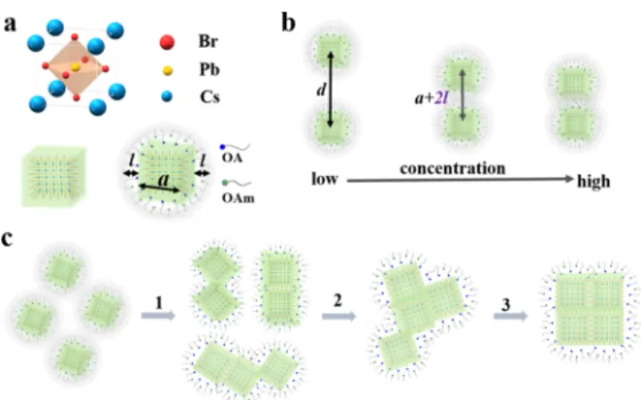
the interactions inside the nanocrystal solution such as entropy, electrostatic force, van der Waals force, and hydrogen bonding forces.37The dominated interaction depends on the competi-tion between the repulsive and attractive forces, which could be controlled by the chain length of ligands, the size and shape of the nanocrystals, and the solvent polarity.38In this work, the CsPbBr3 nanocrystals were synthesized by a modified hot-injection method using oleic acid (OA) and oleylamine (OLA) as surfactants,1,7presenting a cubic shape with a mean size of ∼10 nm (Figure S1,Supporting Information). The surfactant molecules are adsorbed on nanocrystal surfaces via covalent bonds (Figure S2, Supporting Information), forming an organic−inorganic interface which protects the nanocrystal surfaces and facilitates to disperse in solution. Because of the surface-capping ligand chains, there exists a ligand corona around the planar crystalline surfaces, so that the real shape of the nanocrystals when dispersed in solvent is like quasi-spherical,39and the radius (r) should be a/2 + l, (a is the side length of cubic core, l is the length of the ligand chain∼2 nm), as shown in Figure 1a. It implies that besides the core−core
interaction, both the corona−corona and ligand−core inter-actions affect the assembly behavior of the CsPbBr3
nanocryst-als upon solvent evaporation. The corona morphology would change with the variation of the nanocrystal concentration as well as the switch of the interparticle interactions.37 As exhibited inFigure 1b, the interparticle distance (d) decreases with the crowding of the nanoparticles in a certain volume of solvents. At low concentrations, d is larger than a + 2l, when the repulsive potential dominates and noflocculation occurs. The repulsion force is favorable to the monodispersing of the nanoparticles. The nanoparticles suffer from fierce competition between corona−corona repulsion and core−core attraction forces when d equals to a + 2l. With the increase of the concentration, the coronas would first experience the self-compression to avoid the aggregation and then the inter-penetration due to the domination of the attraction force. This is coincident with the general self-aggregation of nanoparticles during the solvent evaporation process.24,26,28,40,41
Figure 1.Schematic illustration of (a) crystal structure, the ligands capped nanocrystal and (b) interaction between nanoparticles change with the concentration. (c) Illustration of the model for solvent-assisted interface engineering: step 1 is the solvent trigger process to obtain one-dimensional assembles, step 2 is to terminate the former process and obtain two-dimensional assemblies, and step 3 represents the thinfilm assembly during solvent evaporation. The corresponding experiment procedures are depicted in Figure S3 (Supporting Information).
As is shown in Figure 1c, taking advantage of the dynamic ligand−surface interface and the sensitivity of ILHPs to solvent polarity, the good solvent was utilized as the assembly trigger (step 1) to conduct the assemble process in a one-dimensional orientation because of the collaboration effect of the hydro-phobic effect and van der Waals interaction.35
Under high density condition, the interparticle distance will get smaller, and the nanoparticles have the potential to orderly assemble to maximize the system’s total entropy.37 A nonsolvent or antisolvent was then employed (step 2) to terminate the one-dimensional assembling process and drive the organization in two-dimensional orientation, by virtue of the maximum of the interparticle attractive forces.35 The solution destabilization makes ligand coronas contract together to screen the poor solvent permeation, and some ligands would desorb from the surface to minimize the corona surface area. In view of the fragile nature of CsPbBr3, the hexane (polarity index is 0.06) and ethyl acetate (EA, polarity index is 4.3) were chosen as the good solvent and the nonsolvent, respectively.36,42 The subsequent discard of the nonsolvent ends the assembly process in the two-dimensional direction and makes the final products possess a finite assembled size as well as the good dispersity and stability in solution, which is beneficial to the thin film fabrication during the drying of solvents (step 3). Therefore, the solvent-assisted surface engineering, activating the nanoparticle self-assembly behaviors, ensures the fabrication of dense and smooth CsPbBr3 nanoparticle thin films. The corresponding experiment details are depicted and described in Figure S3 (Supporting Information).
Thanks to the ionic nature of the CsPbBr3crystal structure,
the crowding nanoparticles could continue to grow and gather together to rearrange their overall appearance. As shown in Figure 2a, the as-synthesized CsPbBr3 nanocrystals exhibit
nanocube morphology, and it seems like, from the whole view, the assembly of the nanocubes into a one-dimensional structure has beenfirst interrupted by growing in planar two-dimensional direction, which is also frozen at the intermediate state resulting in some bigger nanocubes with a size of ∼25 nm. This
phenomenon is very consistent with the expected results from solvent-assisted surface engineering. When treated with the typical antisolvents (e.g., acetone) purification processes, the CsPbBr3 nanoparticles appear to be dispersed in isolation as shown in Figure S1 (Supporting Information).1,7,36 CsPbBr3
nanoparticles processed by the proposed solvent-assisted surface engineering presents distinctly localized assembly in both one-dimensional and two-dimensional directions. For example, as shown in the white circle area in Figure 2a, the adjacent nanoparticles are connected by the means of face-to-face, edge-to-edge, or corner-to-corner contacts.
To get deep insight into the way how the separated nanocubes fuse together, the high-resolution transmission electron microscopy (HRTEM) image in Figure 2b reveals that two independent nanocubes integrate directly, and the well-resolved interfringe distance of 0.45 nm at the combining interface could be indexed to the (010) lattice spacings of the cubic phase (Figure 2b inset), and the assembly process could also be conducted along the −202 direction (Figure S4, Supporting Information). The optical properties could also demonstrate the interconnecting between nanocubes. As shown inFigure 2c, the PL peak of 522 nm is slightly red-shifted from that of pristine CsPbBr3nanoparticles with a PL peak at 520
nm (Figure S5, Supporting Information), which indirectly verifies the size growth of some nanoparticles after the solvent-assisted surface engineering treatment.7 In addition, the decrease of the PLQY from 90% to 58% indicates that the CsPbBr3 nanocubes were assembled at the expense of the
surface ligands.36Meanwhile, the resultant assembled CsPbBr3 nanoparticles still retain good dispersity in the solution (insets in Figure 2c). Remarkably, all these results are in good agreement with what is expected from the proposed assembly mechanism. The CsPbBr3 thin film was fabricated by
spin-coating technique. The scanning electron microscopy (SEM) and atomic force microscopy (AFM) images (Figure 2d,e) demonstrate that the thin film was highly dense and very smooth with a surface roughness of 4.8 nm. Comparatively, the thin film made from unassembled CsPbBr3 nanocrystals
Figure 2.Effect of the solvent-assisted interface engineering on CsPbBr3nanocrystal performances. (a) Low magnification and (b) HRTEM images
of the assembled CsPbBr3nanocrystals; inset is the corresponding fast Fourier transform image. (c) UV−vis absorbance and PL spectra of CsPbBr3
nanocrystals dispersed in hexane and photographs under daylight (left inset) and 365 nm UV light (right inset). (d) SEM and (e) AFM images of the spin-coating-casted CsPbBr3thinfilm. (f) PL spectrum (black solid line) and photograph (under 365 nm UV light) of the CsPbBr3thinfilm.
The PL spectrum in the green dashed line represents CsPbBr3nanocrystals in hexane.
(Figure S6, Supporting Information) is inhomogeneous and rough with a surface roughness of 18 nm (Figure S7, Supporting Information).
The PL emission peak of the solid CsPbBr3 thin film is
almost coincident with that of CsPbBr3solution, as shown in
Figure 2f, which confirmed the assembly performance of the CsPbBr3 nanoparticles. Furthermore, our solvent-assisted surface engineering can conduct the assembly of forming high-quality CsPbBr3 thin films on not only a normal flat surface but also a curved one like the inside surface of a glass vial. The assembly extent could be adjusted by the amount of the good (nonpolar) solvent used in the assembly trigger process. With the enhancement of the assembly degree, the stability of the CsPbBr3 nanocubes in solution generally get reduced because of the increase of the size.36The thinfilm self-assembly took place on the inside surface of the vial bottle during the storage, which is distinctly different from the general nanocrystal aggregation accompanied by the sediments in the bottom of the bottle. Notably, the thinfilm is still very stable even after ultrasonication for 60 min in hexane (Figure S8, Supporting Information), which sheds light on the potential application of CsPbBr3thinfilms on flexible curved surfaces.
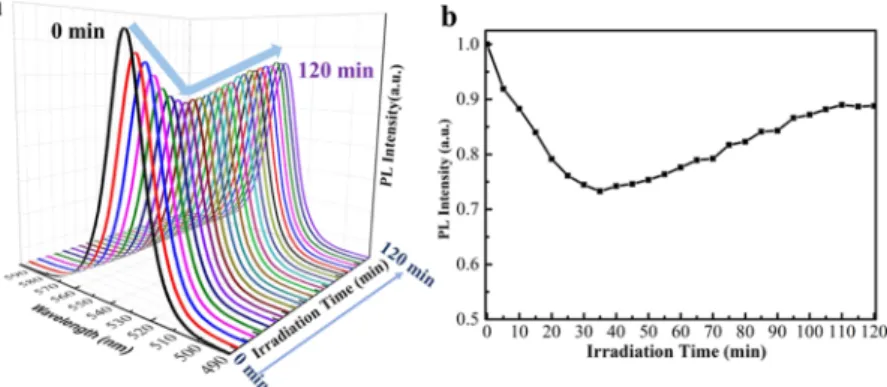
The stability of the CsPbBr3-based thin film against the
photodegradation has been a big concern in the practical device application. To further verify the photostability of the assembled CsPbBr3 thin film, we carried out the in situ PL
monitoring investigation. The experiment setup is schematically illustrated inFigure S9, a He−Cd continuous wave laser (λ =
442 nm) was employed as both the irradiation light and the excitation source, and the excitation intensity was set as 50 mW cm−2with the aid of a tunable attenuator. The solid CsPbBr3
thinfilm was fixed and irradiated for 120 min continuously at ambient atmosphere (26 °C, 60% humidity), and the PL spectra were collected every 5 min. In contrast to the case of CsPbBr3nanoplates where the photon exposure gives rise to
the structure transformation resulting in the emergence of new emission peaks,10the PL peak kept locating at 522 nm and no new emission peak appeared under the uninterrupted laser irradiation, as shown in Figure 3a,b. Meanwhile, the PL intensity suffered from a decrease of about 25% in the first 35 min, which is attributed to the formation of surface and interface trap sites induced by the desorption of surface ligands under the photoillumination.10 After the degradation process, the increase of about 15% of the intensity was traced back to the surface defects healing owing to the recrystallization process. Thefinal PL intensity returned to about 88%, because of which the sustained irradiation-induced thermal effect was also responsible for the decrease of the PL emission intensity.43 The photostability of the localized assembly CsPbBr3thinfilm has been improved about 30% compared with the pristine and unassembled CsPbBr3-based thin film (Figures S10−S12, Supporting Information).
To further demonstrate the effect of solvent-assisted surface engineering on the charge injection into CsPbBr3 thin films,
LEDs based on the assembled CsPbBr3 nanocrystals (device
G1) and unassembled CsPbBr3nanocrystals (device G2) were
Figure 3.Photostability performance of the CsPbBr3thinfilm. (a) In situ PL spectra were collected every 5 min during the continuous irradiation
(excitation wavelength of 442 nm and intensity of 50 mW cm−2). (b) PL intensity versus the light exposure time.
Figure 4.(a) Schematic structure of LEDs. (b) Chemical structure of charge transporting layers. (c) Energy levels of the LEDs.
developed. The device configuration is shown in Figure 4a, composed of multilayers in the following order: indium tin oxide (ITO), poly(ethylenedioxythiophene):polystyrene sulfo-nate (PEDOT:PSS, 40 nm), N,N ′-bis(4-butylphenyl)-N,N′-bis(phenyl)benzidine (poly-TPD, 40 nm), CsPbBr3-emitting layer (20 nm), 2,2 ′,2″-(1,3,5-benzenetriyl)tris-1-phenyl-1H-benzimidazole (TPBi, 35 nm), and Cs2CO3/Al (1/100 nm). Except for the TPBi and LiF/Al layers which were deposited with thermal vacuum technology, all the other layers were fabricated by spin coating layer by layer on a prepatterned ITO transparent anode. The CsPbBr3-emitting layer built on the HTL layer exhibited homogenous density and smooth morphology, with a surface roughness of 4.75 nm (Figures S13 and S14, Supporting Information). The cross-sectional SEM image of the PeLED is depicted in Figure S15 (Supporting Information). Figure 4c shows a schematic illustration of theflat-band energy level diagram of the layers. The poly-TPD layer, serving as both the hole-transporting and the electron-blocking layer, benefits from its specific molecular energy configuration. The highest occupied molecular orbital (HOMO, 5.4 eV) is located between the HOMO of PEDOT:PSS and the valance band of CsPbBr3, while the lowest unoccupied molecular orbital (2.3 eV) is much higher than the CsPbBr3conduction band.44The TPBi layer worked as not only the electron transporting layer but also the hole blocking layer owing to its deep HOMO of 6.2 eV.45Hence, holes and electrons were allowed to recombine effectively in the CsPbBr3-based emitting layer.
The performances of device G1 and device G2 are summarized inFigure 5 andTable 1. The maximum EQE for device G1 is as high as 1.70%, which is about 34-fold higher than that of device G2, as shown inFigure 5a. The remarkable EQE enhancement indicates that the carrier transport proper-ties in the CsPbBr3-emitting layer were significantly improved
because of the effect of the solvent-assisted surface engineering on the thinfilm forming. In addition, the EQE of 1.70% is also higher than those of recently reported representative CsPbBr3 -based LEDs (e.g., 1.49% from Zeng’s group,461.37% from Lee’s
group,47and≤0.93% for others),30,48−53further indicating the advantage of the solvent-assisted surface engineering. It is worthy of noting that the EQE roll-off is quite obvious for both devices G1 and G2, which is a common phenomenon occurring in all-inorganic PeLEDs devices.46−53There are several reasons that could lead to the roll-off case, including the current damage, the charging effect, the Auger decay, and the accumulation of mobile ion-induced luminescence quenching, which calls for further investigation.7,45,54 Both the current density and luminance intensify with the increase of the applied voltage, as presented inFigure 5b. The maximum luminance for device G1 is 1562 cd m−2, which is about 11-fold higher than that for device G2. The corresponding current density for device G1 has also been substantially improved, for instance, from 28 mA cm−2for device G2 to 101 mA cm−2at 14 V. The maximum current efficiency for device G1 shows a maximum of 5.57 cd A−1, which is 31-fold higher than that of device G2 (Figure S16,Supporting Information).55−57
All these results confirm that the charge injection and transport balance have indeed been boosted after the process of solvent-assisted surface engineering. Figure 5c shows that the device gives a very narrow EL emission peak with a fwhm of 16 nm and it is, to the best of our knowledge, the narrowest value among CsPbBr3-based LEDs, which is attributed to the narrow band-edge emission of the CsPbBr3 nanocrystals. It’s obvious
that there is no parasitic emission originated from the charge-transport layers, indicating good electron and hole blocking functions of both poly-TPD and TPBi layers. It shows inFigure 5d that the maximum power efficiency of device G1 is 1.59 lm Figure 5.Performances of the device G1 and the control device G2. (a) EQE as a function of current density. (b) Current density and luminance versus driving voltage. (c) Normalized EL spectrum at an applied voltage of 10 V and a photograph of device G1 under bias (inset). (d) Power efficiency as a function of current density.
Table 1. Summary of the Performances of LEDs
device EQEmaxa (%) CEmaxb (cd A−1) PEmaxc (lm W−1) Lmaxd (cd m−2) fwhm (nm) G1 1.70 5.57 1.59 1562 16 G2 0.05 0.18 0.04 140 16
aMaximum EQE. bMaximum CE. cMaximum PE. dMaximum luminance.
W−1, which is 40-fold higher than that of device G2 and further demonstrates the merit of the proposed strategy.
The operational stability of PeLEDs is a critical issue, which is rarely reported in thisfield. To deeply comprehend the as-fabricated PeLEDs, the stability under continuous operation at a constant voltage of 10 V has been evaluated in ambient air at room temperature. The half-lifetime (T50) is defined as the time for the luminance decreasing to 50% of the starting luminance (L0). As shown in Figure S17 (Supporting Information), the T50 of device G1 is 630 s, which is better than previous
all-inorganic PeLEDs.58,59On the other hand, the T50of device G2 is only 35 s at the same initial luminance, which is 18-fold shorter than that of device G1, further indicating the advantage of self-assembled CsPbBr3 thin films. The reproducibility of
devices is reasonably high. It is demonstrated that the EQE values of over 80% of PeLED devices based on the self-assembled CsPbBr3thinfilm were higher than 1.4%, as shown by the histograms of maximum EQE taken from 18 devices (Figure S18,Supporting Information).
■
CONCLUSIONSIn summary, we have proposed and demonstrated a facile strategy, solvent-assisted surface engineering, to improve the quality of nanocrystal thinfilms for LED application. Solvents with different polarities were collaboratively utilized to obtain CsPbBr3nanocrystal assemblies. The influence of the
solvent-assisted surface engineering strategy on the morphology and optical and electronic properties of the nanocrystal thin films has been investigated. The solid CsPbBr3thinfilms fabricated from the as-processed solution are highly dense and smooth, favorable for both charge injection and electrical transport for device application. Meanwhile, the thinfilms’ photostability has been improved about 30% compared to those made from pristine and unassembled CsPbBr3nanoparticle solutions. Our
strategy has been clearly validated by successful fabrication of CsPbBr3 LEDs with remarkably high performance.
Conse-quently, a 34-fold EQE enhancement (up to 1.70%) has been achieved from solution-processed CsPbBr3 LEDs. The
corresponding luminance, current efficiency, and the power efficiency were 11-, 31-, and 40-fold, respectively, which are much better than control devices. The fwhm of the EL spectrum is only 16 nm, which is the narrowest among CsPbBr3
LEDs. Our method is facile and reliable, thus the work shall be insightful for developing optoelectronic devices from the rising material system-inorganic metal lead halide perovskites.
■
EXPERIMENTAL METHODSChemicals. All reagents were used as received without further purification. 1-Octadecene (ODE, technical grade, 90%), OA (technical grade, 90%), OLA (technical grade, 70%), cesium carbonate (Cs2CO3, 99.9% trace metals basis), lead chloride (PbCl2, 99.999%
trace metals basis), lead bromide (PbBr2, 99.999% trace metals basis),
lead iodide (PbI2, 99.999% trace metals basis), EA (anhydrous,
99.8%), toluene (anhydrous), and octane (anhydrous,≥99%) were all purchased from Sigma-Aldrich. Hexane (HPLC grade) was purchased from Fishier Scientific.
Synthesis of Cs-Oleate. Cs2CO3(0.814 g), 40 mL ODE, and 2.5
mL OA were loaded into a 100 mL three-neckflask, dried at 120 °C for 1 h, and then the temperature was raised to 150°C under N2flow
until all Cs2CO3reacted with OA. It needs to be preheated to 150°C
before injection.
Synthesis of CsPbBr3QDs. ODE (15 mL), 3 mL of OAm, 1.5 mL
of OA, and PbBr2(0.2 g) were loaded into a 50 mL three-neckflask,
degassed, and dried under vacuum for 20 min at 120°C. During this
process, the PbBr2 precursor dissolved completely and mixed
thoroughly with the reaction solution. Then, with the protection of N2atmosphere, the reaction temperature was raised to 170°C with a
rate of 15°C min−1. The preheated Cs-oleate solution (0.66 mL, 0.125 M in ODE) was injected swiftly, 8 s later, and the reaction mixture was cooled down with a rate of 15°C min−1to the room temperature.
Processes for Partial Connected of CsPbBr3 QDs. The
purification process contains mainly three steps: hexane was first added into the crude solution with a volume ratio of (1:10), and the precipitate was collected after centrifugation (8500 rpm, 5 min) and dispersed in 4 mL hexane. Then, 16 mL of EA was added into 4 mL of hexane solution with a volume ratio of 4:1 and the precipitate was collected after centrifugation (8500 rpm, 5 min) and redispersed in 4 mL of hexane. Thefinal product was saved as stock solution for the LED fabrication.
Optical Characterization. UV−vis absorption spectra were collected with a UV-1800 spectrometer. The PLQYs of solution samples were obtained at an excitation wavelength of 442 nm with the absolute quantum efficiency measurement system-QE 200B (Otsuka Electronic Co., Ltd.) To characterize the photostability of the thinfilm sample, the samples were fixed and irradiated by the He−Cd continuous wave laser light (442 nm) for 90 min. The PL signal was dispersed by a monochromator and detected by a photomultiplier tube.
Device Fabrication and Characterization. PEDOT:PSS solutions (filtered through a 0.45 μm filter) were spin-coated onto the ITO-coated glass substrates (having a sheet resistance of 15 Ω sq−1) at 4000 rpm for 60 s and baked at 150°C for 30 min. The hole transporting and electron blocking layers were prepared by spin-coating poly-TPD chlorobenzene solution (concentration: 8 mg mL−1) at 2000 rpm for 45 s. Perovskite nanocrystals were deposited by spin-coating at 2000 rpm for 45 s. Afterward, the samples were transferred into a vacuum thermal evaporation chamber to deposit other organic materials and cathode. Without breaking the vacuum, the TPBi, Cs2CO3, and Al layers were thermally deposited at a base
pressure of 4.0× 10⁻⁴Pa. The thicknesses of layers were controlled by the quartz crystal oscillators. After preparation under a nitrogen atmosphere using epoxy glue and glass slides, all devices were encapsulated immediately. The emission area of all devices is 1× 1 mm2as defined by the overlapping area of the anode and the cathode.
The EL spectra were recorded via a PR705 Spectra Scan spectrometer. By utilizing a computer-controlled source meter (Keithley source measure unit 2400), the current density−voltage−luminance (I−V−L) properties were measured simultaneously. Accordingly, the CE and PE were obtained. EQE values were calculated from the luminance, current density, and EL spectrum.
■
ASSOCIATED CONTENT*
S Supporting InformationThe Supporting Information is available free of charge on the ACS Publications websiteat DOI:10.1021/acsami.8b06105.
Additionalfigures (PDF)
■
AUTHOR INFORMATION Corresponding Authors *E-mail:[email protected](H.V.D.). *E-mail:[email protected](H.G.). *E-mail:[email protected](H.S.). ORCIDHilmi Volkan Demir:0000-0003-1793-112X
Haoshuang Gu:0000-0003-1232-2499
Handong Sun: 0000-0002-2261-7103
Author Contributions
¶L.W. and B.L. make contribution equally.
Notes
The authors declare no competingfinancial interest.
■
ACKNOWLEDGMENTSThis work was supported by the Singapore Ministry of Education through the Academic Research Fund under Projects MOE2016-T2-1-054, Tier 1-RG105/16 and Tier 1-RG92/15 a n d C h i n a S c h o l a r s h i p C o u n c i l ( 2 0 1 6 3 1 0 0 , n o . 201608420137). Thanks to the support of the National Research Foundation, Prime Minister’s Office, Singapore under its Competitive Research program (NRF-CRP14-2014-03), its Investigatorship program (NRF-NRFI2016-08) and the Singapore Agency for Science, Technology and Research (A*STAR) SERC Pharos Program under grant no. 152 73 00025. H.V.D. gratefully acknowledges TUBA-GEBIP.
■
REFERENCES(1) Protesescu, L.; Yakunin, S.; Bodnarchuk, M. I.; Krieg, F.; Caputo, R.; Hendon, C. H.; Yang, R. X.; Walsh, A.; Kovalenko, M. V. Nanocrystals of Cesium Lead Halide Perovskites (CsPbX3, X = Cl, Br,
and I): Novel Optoelectronic Materials Showing Bright Emission with Wide Color Gamut. Nano Lett. 2015, 15, 3692−3696.
(2) Ramasamy, P.; Lim, D.-H.; Kim, B.; Lee, S.-H.; Lee, M.-S.; Lee, J.-S. All-inorganic Cesium Lead Halide Perovskite Nanocrystals for Photodetector Applications. Chem. Commun. 2015, 52, 2067−2070.
(3) Li, X.; Wu, Y.; Zhang, S.; Cai, B.; Gu, Y.; Song, J.; Zeng, H. CsPbX3Quantum Dots for Lighting and Displays: Room-Temperature
Synthesis, Photoluminescence Superiorities, Underlying Origins and White Light-Emitting Diodes. Adv. Funct. Mater. 2016, 26, 2435− 2445.
(4) Parobek, D.; Dong, Y.; Qiao, T.; Rossi, D.; Son, D. H. Photoinduced Anion Exchange in Cesium Lead Halide Perovskite Nanocrystals. J. Am. Chem. Soc. 2017, 139, 4358−4361.
(5) Rakita, Y.; Kedem, N.; Gupta, S.; Sadhanala, A.; Kalchenko, V.; Böhm, M. L.; Kulbak, M.; Friend, R. H.; Cahen, D.; Hodes, G. Low-Temperature Solution-Grown CsPbBr3 Single Crystals and Their
Characterization. Cryst. Growth Des. 2016, 16, 5717−5725.
(6) Nedelcu, G.; Protesescu, L.; Yakunin, S.; Bodnarchuk, M. I.; Grotevent, M. J.; Kovalenko, M. V. Fast Anion-Exchange in Highly Luminescent Nanocrystals of Cesium Lead Halide Perovskites (CsPbX3, X = Cl, Br, I). Nano Lett. 2015, 15, 5635−5640.
(7) Song, J.; Li, J.; Li, X.; Xu, L.; Dong, Y.; Zeng, H. Quantum Dot Light-Emitting Diodes Based on Inorganic Perovskite Cesium Lead Halides (CsPbX3). Adv. Mater. 2015, 27, 7162−7167.
(8) Berends, A. C.; de Mello Donega, C. Ultrathin One- and Two-Dimensional Colloidal Semiconductor Nanocrystals: Pushing Quan-tum Confinement to the Limit. J. Phys. Chem. Lett. 2017, 8, 4077− 4090.
(9) Zhang, D.; Eaton, S. W.; Yu, Y.; Dou, L.; Yang, P. Solution-Phase Synthesis of Cesium Lead Halide Perovskite Nanowires. J. Am. Chem. Soc. 2015, 137, 9230−9233.
(10) Wang, Y.; Li, X.; Sreejith, S.; Cao, F.; Wang, Z.; Stuparu, M. C.; Zeng, H.; Sun, H. Photon Driven Transformation of Cesium Lead Halide Perovskites from Few-Monolayer Nanoplatelets to Bulk Phase. Adv. Mater. 2016, 28, 10637−10643.
(11) Akkerman, Q. A.; Motti, S. G.; Kandada, A. R. S.; Mosconi, E.; D’Innocenzo, V.; Bertoni, G.; Marras, S.; Kamino, B. A.; Miranda, L.; De Angelis, F.; Petrozza, A.; Prato, M.; Manna, L. Solution Synthesis Approach to Colloidal Cesium Lead Halide Perovskite Nanoplatelets with Monolayer-Level Thickness Control by a Solution Synthesis Approach. J. Am. Chem. Soc. 2016, 138, 1010−1016.
(12) Wang, Y.; Sun, H. All-Inorganic Metal Halide Perovskite Nanostructures: From Photophysics to Light-Emitting Applications. Small Methods 2017, 2, 1700252.
(13) Zhang, X.; Sun, C.; Zhang, Y.; Wu, H.; Ji, C.; Chuai, Y.; Wang, P.; Wen, S.; Zhang, C.; Yu, W. W. Bright Perovskite Nanocrystal Films for Efficient Light-Emitting Devices. J. Phys. Chem. Lett. 2016, 7, 4602−4610.
(14) Zhang, X.; Lin, H.; Huang, H.; Reckmeier, C.; Zhang, Y.; Choy, W. C. H.; Rogach, A. L. Enhancing the Brightness of Cesium Lead
Halide Perovskite Nanocrystal Based Green Light-Emitting Devices through the Interface Engineering with Perfluorinated Ionomer. Nano Lett. 2016, 16, 1415−1420.
(15) Zhang, L.; Yang, X.; Jiang, Q.; Wang, P.; Yin, Z.; Zhang, X.; Tan, H.; Yang, Y.; Wei, M.; Sutherland, B. R.; Sargent, E. H.; You, J. Ultra-bright and Highly Efficient Inorganic Based Perovskite Light-emitting Diodes. Nat. Commun. 2017, 8, 15640.
(16) Kim, Y.-H.; Wolf, C.; Kim, Y.-T.; Cho, H.; Kwon, W.; Do, S.; Sadhanala, A.; Park, C. G.; Rhee, S.-W.; Im, S. H.; Friend, R. H.; Lee, T.-W. Highly Efficient Light-Emitting Diodes of Colloidal Metal− Halide Perovskite Nanocrystals beyond Quantum Size. ACS Nano 2017, 11, 6586−6593.
(17) Yang, B.; Zhang, F.; Chen, J.; Yang, S.; Xia, X.; Pullerits, T.; Deng, W.; Han, K. Ultrasensitive and Fast All-Inorganic Perovskite-Based Photodetector via Fast Carrier Diffusion. Adv. Mater. 2017, 29, 1703758.
(18) Wang, H.; Kim, D. H. Perovskite-based Photodetectors: Materials and Devices. Chem. Soc. Rev. 2017, 46, 5204−5236.
(19) Akkerman, Q. A.; Gandini, M.; Di Stasio, F.; Rastogi, P.; Palazon, F.; Bertoni, G.; Ball, J. M.; Prato, M.; Petrozza, A.; Manna, L. Strongly Emissive Perovskite Nanocrystal Inks for High-Voltage Solar Cells. Nat. Energy 2016, 2, 16194.
(20) Zhang, X.; Zhang, J.; Phuyal, D.; Du, J.; Tian, L.; Öberg, V. A.; Johansson, M. B.; Cappel, U. B.; Karis, O.; Liu, J.; Rensmo, H.; Boschloo, G.; Johansson, E. M. J. Inorganic CsPbI3Perovskite Coating
on PbS Quantum Dot for Highly Efficient and Stable Infrared Light Converting Solar Cells. Adv. Energy Mater. 2017, 8, 1702049.
(21) Yakunin, S.; Protesescu, L.; Krieg, F.; Bodnarchuk, M. I.; Nedelcu, G.; Humer, M.; De Luca, G.; Fiebig, M.; Heiss, W.; Kovalenko, M. V. Low-threshold Amplified Spontaneous Emission and Lasing from Colloidal Nanocrystals of Caesium Lead Halide Perovskites. Nat. Commun. 2015, 6, 8056.
(22) Wang, Y.; Li, X.; Nalla, V.; Zeng, H.; Sun, H. Solution-Processed Low Threshold Vertical Cavity Surface Emitting Lasers from All-Inorganic Perovskite Nanocrystals. Adv. Funct. Mater. 2017, 27, 1605088.
(23) Wang, Y.; Li, X.; Song, J.; Xiao, L.; Zeng, H.; Sun, H. All-Inorganic Colloidal Perovskite Quantum Dots: A New Class of Lasing Materials with Favorable Characteristics. Adv. Mater. 2015, 27, 7101− 7108.
(24) Boles, M. A.; Ling, D.; Hyeon, T.; Talapin, D. V. The Surface Science of Nanocrystals. Nat. Mater. 2016, 15, 141−153.
(25) Cho, H.; Jeong, S.-H.; Park, M.-H.; Kim, Y.-H.; Wolf, C.; Lee, C.-L.; Heo, J. H.; Sadhanala, A.; Myoung, N.; Yoo, S.; Im, S. H.; Friend, R. H.; Lee, T.-W. Overcoming the Electroluminescence Efficiency Limitations of Perovskite Light-emitting Diodes. Science 2015, 350, 1222−1225.
(26) De Roo, J.; Ibáñez, M.; Geiregat, P.; Nedelcu, G.; Walravens, W.; Maes, J.; Martins, J. C.; Van Driessche, I.; Kovalenko, M. V.; Hens, Z. Highly Dynamic Ligand Binding and Light Absorption Coefficient of Cesium Lead Bromide Perovskite Nanocrystals. ACS Nano 2016, 10, 2071−2081.
(27) Kang, J.; Wang, L.-W. High Defect Tolerance in Lead Halide Perovskite CsPbBr3. J. Phys. Chem. Lett. 2017, 8, 489−493.
(28) ten Brinck, S.; Infante, I. Surface Termination, Morphology, and Bright Photoluminescence of Cesium Lead Halide Perovskite Nanocrystals. ACS Energy Lett. 2016, 1, 1266−1272.
(29) Li, X.; Yu, D.; Cao, F.; Gu, Y.; Wei, Y.; Wu, Y.; Song, J.; Zeng, H. Healing All-Inorganic Perovskite Films via Recyclable Dissolution-Recyrstallization for Compact and Smooth Carrier Channels of Optoelectronic Devices with High Stability. Adv. Funct. Mater. 2016, 26, 5903−5912.
(30) Zhang, X.; Wang, W.; Xu, B.; Liu, S.; Dai, H.; Bian, D.; Chen, S.; Wang, K.; Sun, X. W. Thin Film Perovskite Light-emitting Diode Based on CsPbBr3Powders and Interfacial Engineering. Nano Energy
2017, 37, 40−45.
(31) Zhao, L.; Yeh, Y.-W.; Tran, N. L.; Wu, F.; Xiao, Z.; Kerner, R. A.; Lin, Y. L.; Scholes, G. D.; Yao, N.; Rand, B. P. In Situ Preparation
of Metal Halide Perovskite Nanocrystal Thin Films for Improved Light-Emitting Devices. ACS Nano 2017, 11, 3957−3964.
(32) Yu, J. C.; Kim, D. W.; Kim, D. B.; Jung, E. D.; Lee, K.-S.; Lee, S.; Nuzzo, D. D.; Kim, J.-S.; Song, M. H. Effect of the Solvent Used for Fabrication of Perovskite Films by Solvent Dropping on Performance of Perovskite Light-emitting Diodes. Nanoscale 2017, 9, 2088−2094.
(33) Chiba, T.; Hoshi, K.; Pu, Y.-J.; Takeda, Y.; Hayashi, Y.; Ohisa, S.; Kawata, S.; Kido, J. High-Efficiency Perovskite Quantum-Dot Light-Emitting Devices by Effective Washing Process and Interfacial Energy Level Alignment. ACS Appl. Mater. Interfaces 2017, 9, 18054− 18060.
(34) Pan, J.; Quan, L. N.; Zhao, Y.; Peng, W.; Murali, B.; Sarmah, S. P.; Yuan, M.; Sinatra, L.; Alyami, N. M.; Liu, J.; Yassitepe, E.; Yang, Z.; Voznyy, O.; Comin, R.; Hedhili, M. N.; Mohammed, O. F.; Lu, Z. H.; Kim, D. H.; Sargent, E. H.; Bakr, O. M. Highly Efficient Perovskite-Quantum-Dot Light-Emitting Diodes by Surface Engineering. Adv. Mater. 2016, 28, 8718−8725.
(35) Soetan, N.; Erwin, W. R.; Tonigan, A. M.; Walker, D. G.; Bardhan, R. Solvent-Assisted Self-Assembly of CsPbBr3 Perovskite
Nanocrystals into One-Dimensional Superlattice. J. Phys. Chem. C 2017, 121, 18186−18194.
(36) Li, J.; Xu, L.; Wang, T.; Song, J.; Chen, J.; Xue, J.; Dong, Y.; Cai, B.; Shan, Q.; Han, B.; Zeng, H. 50-Fold EQE Improvement up to 6.27% of Solution-Processed All-Inorganic Perovskite CsPbBr3QLEDs
via Surface Ligand Density Control. Adv. Mater. 2017, 29, 1603885. (37) Boles, M. A.; Engel, M.; Talapin, D. V. Self-Assembly of Colloidal Nanocrystals: From Intricate Structures to Functional Materials. Chem. Rev. 2016, 116, 11220−11289.
(38) Cademartiri, L.; Bishop, K. J. M.; Snyder, P. W.; Ozin, G. A. Using Shape for Self-assembly. Philos. Trans. R. Soc., A 2012, 370, 2824−2847.
(39) Ravi, V. K.; Santra, P. K.; Joshi, N.; Chugh, J.; Singh, S. K.; Rensmo, H.; Ghosh, P.; Nag, A. Origin of the Substitution Mechanism for the Binding of Organic Ligands on the Surface of CsPbBr3
Perovskite Nanocubes. J. Phys. Chem. Lett. 2017, 8, 4988−4994. (40) Sperling, R. A.; Parak, W. J. Surface Modification, Functionaliza-tion and BioconjugaFunctionaliza-tion of Colloidal Inorganic Nanoparticles. Philos. Trans. R. Soc., A 2010, 368, 1333−1383.
(41) Pradhan, N.; Reifsnyder, D.; Xie, R.; Aldana, J.; Peng, X. Surface Ligand Dynamics in Growth of Nanocrystals. J. Am. Chem. Soc. 2007, 129, 9500−9509.
(42) Swarnkar, A.; Marshall, A. R.; Sanehira, E. M.; Chernomordik, B. D.; Moore, D. T.; Christians, J. A.; Chakrabarti, T.; Luther, J. M. Quantum Dot−Induced Phase Stabilization of a-CsPbI3Perovskite for
High-efficiency Photovoltaics. Science 2016, 354, 92−95.
(43) Chen, J.; Liu, D.; Al-Marri, M. J.; Nuuttila, L.; Lehtivuori, H.; Zheng, K. Photo-stability of CsPbBr3 Perovskite Quantum Dots for
Optoelectronic Application. Sci. China Mater. 2016, 59, 719−727. (44) Wang, M.; Hill, I. G. Fluorinated Alkyl Phosphonic Acid SAMs Replace PEDOT: PSS in Polymer Semiconductor Devices. Org. Electron. 2012, 13, 498−505.
(45) Liu, B.; Nie, H.; Zhou, X.; Hu, S.; Luo, D.; Gao, D.; Zou, J.; Xu, M.; Wang, L.; Zhao, Z.; Qin, A.; Peng, J.; Ning, H.; Cao, Y.; Tang, B. Z. Manipulation of Charge and Exciton Distribution Based on Blue Aggregation-Induced Emission Fluorophors: A Novel Concept to Achieve High-Performance Hybrid White Organic Light-Emitting Diodes. Adv. Funct. Mater. 2016, 26, 776−783.
(46) Zou, S.; Liu, Y.; Li, J.; Liu, C.; Feng, R.; Jiang, F.; Li, Y.; Song, J.; Zeng, H.; Hong, M.; Chen, X. Stabilizing Cesium Lead Halide Perovskite Lattice through Mn (II) Substitution for Air-Stable Light-Emitting Diodes. J. Am. Chem. Soc. 2017, 139, 11443−11450.
(47) Cho, H.; Wolf, C.; Kim, J. S.; Yun, H. J.; Bae, J. S.; Kim, H.; Heo, J.-M.; Ahn, S.; Lee, T.-W. High-Efficiency Solution-Processed Inorganic Metal Halide Perovskite Light-Emitting Diodes. Adv. Mater. 2017, 29, 1700579.
(48) Van Le, Q.; Kim, J. B.; Kim, S. Y.; Lee, B.; Lee, D. R. Structural Investigation of Cesium Lead Halide Perovskites for High-Efficiency Quantum Dot Light-Emitting Diodes. J. Phys. Chem. Lett. 2017, 8, 4140−4147.
(49) Zhang, X.; Xu, B.; Wang, W.; Liu, S.; Zheng, Y.; Chen, S.; Wang, K.; Sun, X. W. Plasmonic Perovskite Light-Emitting Diodes Based on the Ag-CsPbBr3System. ACS Appl. Mater. Interfaces 2017, 9, 4926−
4931.
(50) Shan, Q.; Li, J.; Song, J.; Zou, Y.; Xu, L.; Xue, J.; Dong, Y.; Huo, C.; Chen, J.; Han, B.; Zeng, H. All-inorganic Quantum-dot Light-emitting Diodes Based on Perovskite Emitters with Low Turn-on Voltage and High Humidity Stability. J. Mater. Chem. C 2017, 5, 4565−4570.
(51) Wei, S.; Yang, Y.; Kang, X.; Wang, L.; Huang, L.; Pan, D. Homogeneous Synthesis and Electroluminescence Device of Highly Luminescent CsPbBr3 Perovskite Nanocrystals. Inorg. Chem. 2017, 56, 2596−2601.
(52) Van Le, Q.; Park, M.; Sohn, W.; Jang, H. W.; Kim, S. Y. Investigation of Energy Levels and Crystal Structures of Cesium Lead Halides and Their Application in Full-Color Light-Emitting Diodes. Adv. Electron. Mater. 2017, 3, 1600448.
(53) Du, X.; Wu, G.; Cheng, J.; Dang, H.; Ma, K.; Zhang, Y.-W.; Tan, P.-F.; Chen, S. High-Quality CsPbBr3 Perovskite Nanocrystals for
Quantum Dot Light-emitting Diodes. RSC Adv. 2017, 7, 10391− 10396.
(54) Liu, B.; Wang, L.; Gao, D.; Xu, M.; Zhu, X.; Zou, J.; Lan, L.; Ning, H.; Peng, J.; Cao, Y. Harnessing charge and exciton distribution towards extremely high performance: the critical role of guests in single-emitting-layer white OLEDs. Mater. Horiz. 2015, 2, 536−544.
(55) Shi, Z.; Li, Y.; Zhang, Y.; Chen, Y.; Li, X.; Wu, D.; Xu, T.; Shan, C.; Du, G. High-efficiency and air-stable perovskite quantum dots light-emitting diodes with an all-inorganic heterostructure. Nano Lett. 2017, 17, 313−321.
(56) Shi, Z.; Li, S.; Li, Y.; Ji, H.; Li, X.; Wu, D.; Xu, T.; Chen, Y.; Tian, Y.; Zhang, Y.; Shan, C.; Du, G. A Strategy of Solution-Processed All-Inorganic-Heterostructure for Humidity/Temperature-Stable Per-ovskite Quantum Dot Light-Emitting Diodes. ACS Nano 2018, 12, 1462−1472.
(57) Shi, Z.; Li, Y.; Li, S.; Li, X.; Wu, D.; Xu, T.; Tian, Y.; Chen, Y.; Zhang, Y.; Zhang, B.; Shan, C.; Du, G. Localized Surface Plasmon Enhanced All-Inorganic Perovskite Quantum Dot Light-Emitting Diodes Based on Coaxial Core/Shell Heterojunction Architecture. Adv. Funct. Mater. 2018, 28, 1707031.
(58) Zhang, X.; Lin, H.; Huang, H.; Reckmeier, C.; Zhang, Y.; Choy, W. C. H.; Rogach, A. L. Enhancing the brightness of cesium lead halide perovskite nanocrystal based green light-emitting devices through the interface engineering with perfluorinated ionomer. Nano Lett. 2016, 2, 1415−1420.
(59) Liu, B.; Wang, L.; Gu, H.; Sun, H.; Demir, H. V. Highly Efficient Green Light-Emitting Diodes from All-Inorganic Perovskite Nano-crystals Enabled by a New Electron Transport Layer. Adv. Opt. Mater. 2018, 1800220.