LWIR all-atomic layer deposition
ZnO bilayer microbolometer for
thermal imaging
Muhammet Poyraz
Kazim Gorgulu
Zulkarneyn Sisman
Mahmud Yusuf Tanrikulu
Ali Kemal Okyay
Muhammet Poyraz, Kazim Gorgulu, Zulkarneyn Sisman, Mahmud Yusuf Tanrikulu, Ali Kemal Okyay, “LWIR all-atomic layer deposition ZnO bilayer microbolometer for thermal imaging,” Opt. Eng.
LWIR all-atomic layer deposition ZnO bilayer
microbolometer for thermal imaging
Muhammet Poyraz,a,bKazim Gorgulu,bZulkarneyn Sisman,bMahmud Yusuf Tanrikulu,c,*and Ali Kemal Okyayb,†
aStanford University, Department of Electrical Engineering, Stanford, California, United States bBilkent University, Department of Electrical and Electronics Engineering, Ankara, Turkey
cAdana Science and Technology University, Department of Electrical-Electronics Engineering, Adana, Turkey
Abstract. We propose an all-ZnO bilayer microbolometer, operating in the long-wave infrared regime that can be implemented by consecutive atomic layer deposition growth steps. Bilayer design of the bolometer provides very high absorption coefficients compared to the same thickness of a single ZnO layer. High absorptivity of the bilayer structure enables higher performance (lower noise equivalent temperature difference and time constant values) compared to single-layer structure. We observe these results computationally by conducting both optical and thermal simulations.© 2017 Society of Photo-Optical Instrumentation Engineers (SPIE) [DOI:10.1117/1.OE.56.3.037106]
Keywords: uncooled infrared imaging; microbolometers; zinc oxide; atomic layer deposition.
Paper 161781 received Nov. 14, 2016; accepted for publication Mar. 2, 2017; published online Mar. 15, 2017.
1 Introduction
Infrared imaging systems, on the basis of the technology, are broadly classified into cooled and uncooled detectors. The cooled ones, also known as photon detectors, offer high per-formance but they require cryogenic cooling. Therefore, in comparison with photon detectors, uncooled infrared detec-tors are suitable for low cost applications with relatively lower performance.1 Microbolomoters are the dominant uncooled infrared detector technology with more than 95% of the market share in 2010, and they are consumed in larger volumes than all other IR array technologies together in 2014.2,3 A microbolometer mainly consists of active and absorber layers and support arms. Absorber layer absorbs electromagnetic radiation and this increases the temperature of the system. Resulting temperature increase is measured with thermally sensitive active layer by means of change in the resistance. Conventional bolometers use VOx andα-Si as active layer and silicon nitride as absorber layer. Using different materials for active and absorber layers increases production steps and complexity and, therefore, increases the production cost. More recently all-ZnO microbolometer structure which combines both active and absorber layers in a single layer was proposed as a low cost alternative.4 In this paper, we propose an all atomic layer deposition (ALD) grown ZnO bilayer microbolometer, which delivers improved performance above the fundamental limit of a sin-gle layer device (Fig.1). An important metric that determines the performance of the bolometer is the thermal time con-stant. Time constant is directly proportional to the heat capacity of the sensitive area of the pixel and is inversely proportional to the thermal conductance of the support structure.5 Thermal time constant determines the speed of the detector and to achieve high resolution, smaller time con-stants are needed, considering that the frame rate of the sys-tem is constant. Also, detectors with small time constants are
preferred for very high speed applications such as missile tracking.4
Another important performance parameter of a microbol-ometer is noise equivalent temperature difference (NETD)5 expressed as EQ-TARGET;temp:intralink-;e001;326;454 NETD¼ 4F 2V n τ0ADRVðΔP∕ΔTÞλ1−λ2 ; (1) EQ-TARGET;temp:intralink-;e002;326;408 RV¼ ηIdαRd G ; (2)
whereF is the focal ratio of the optics, Vn is the total noise voltage of the detector,τ0 is the transmission of the optics, AD is the active detector area, RV is the responsivity, and ðΔP∕ΔTÞλ1−λ2is the change of power per unit area radiated by a blackbody at temperatureT, in specified band. In the voltage responsivity equation,η is the absorption coefficient, Idis the detector current,α is the temperature coefficient of resistance (TCR) value,Rdis the detector resistance, andG is the thermal conductance.
Smaller NETD signifies better performance and to decrease NETD, conductance can be reduced. However, reducing thermal conductance increases the time constant. Based on the trade-off between NETD and time constant, a new figure of merit is defined as NETD-time constant product.4
EQ-TARGET;temp:intralink-;e003;326;207
FOM¼ NETD × τ: (3)
Using alternative materials with higher values of TCR and new designs that give high absorption coefficient can also reduce NETD without compromising thermal conductivity. Optical simulations of simple bilayer bolometers were per-formed using finite difference time domain (FDTD) method (FDTD Solutions by Lumerical Inc.) and absorption coeffi-cient was extracted. According to the results of optical sim-ulations, thermal simulations are performed using finite *Address all correspondence to: Mahmud Yusuf Tanrikulu, E-mail:
element method (Coventorware), and NETD and time constant values are calculated.
2 Optical Simulations
Recent studies show possibilities of using ZnO in microbol-ometer applications since it shows a high value of TCR and high absorption in long-wave infrared (LWIR) band for sin-gle-layer ZnO structures.4,6 ALD-deposited ZnO exhibits high TCR value when deposited at 120°C while ZnO layers deposited at 250°C show higher optical absorption but near zero TCR.6Here, we present possible uses of consecu-tively deposited bilayer ZnO structures that have different optical and electrical properties6without compromising from simplicity. Proposed bilayer absorber structures consist of 120°C grown ZnO on the top (for high TCR), Al2O3 insu-lator layer in the middle, and 250°C grown ZnO on the bot-tom (for higher optical absorption), and all layers grown by ALD consecutively. Single-layer reference structures contain only one layer of 120°C ALD grown ZnO (Fig. 2). These absorber structures are then suspended on top of a metal reflector layer to assume a generic microbolometer shape. Optical constants of ZnO films that are grown in different temperatures are taken from the previous experiments.6
In order to acquire absorption spectra of reference struc-tures and proposed bilayer ZnO strucstruc-tures, electromagnetic simulations are conducted using FDTD technique. Since proposed structures do not have any variation in thez-axis, a two-dimensional simulation setup is chosen as shown in Fig. 2. On the x-axis, periodic boundary conditions are assumed. On the y-axis, bottom boundary is chosen as a perfect reflector to simulate the metal beneath the microbol-ometer structure. On the top, a perfectly matched layer is assumed. The structure is illuminated with a normally inci-dent plane wave source where the wavelength spans the LWIR band (8 to 12μm). A field monitor is placed 1 μm above the plane wave source in order to calculate the total absorption of the structure. Due to the presence of the bottom reflector boundary, optical power can either be absorbed or reflected to the top. Therefore, total absorbed power can be found as (Pabs¼ 1 − Pref) where Pref is the ratio of total reflected power to the incident power.
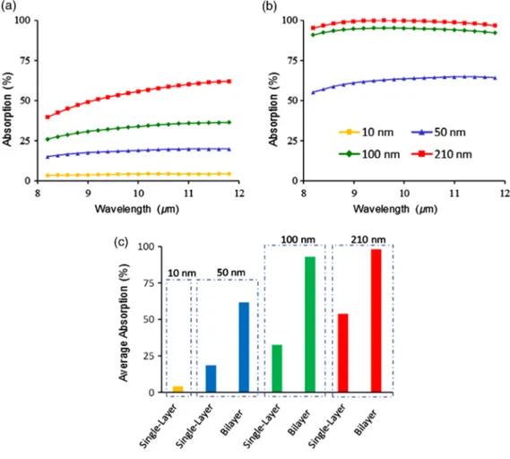
A parameter sweep is conducted for bilayer structure to determine the optimum structure where the ratio of average absorption to thickness is maximized. The thicknesses of the top layer (t1) and bottom layer (t2) are varied from 10 to 200 nm. The gap between absorber structure and metallic bottom boundary is swept from 200 nm to 4μm and at 2.6μm it appeared that the absorption is maximized. Therefore, the gap is assumed 2.6μm thick and kept constant for all simulations. For each bilayer structure, a reference structure of single layer ZnO with the same total thickness is also simulated. Three structures were chosen for further investigation with t1− tAl2O3− t2: 30–10–10 nm, 80–10–
10 nm, 100–10–100 nm. Reference structures with the same total thicknesses (50, 100, and 210 nm) as well as a 10-nm-thick reference structure are simulated. As can be seen in Fig. 3, bilayer structures exhibit dramatic increase in average absorption compared to single-layer structures with the same thickness. As the thickness of the reference single-layer structure increases, the absorption also increases linearly as expected. These results show that a bilayer as thin as 50 nm absorbs more than a much thicker (210 nm) single layer, which is very promising for microbolometer applications.
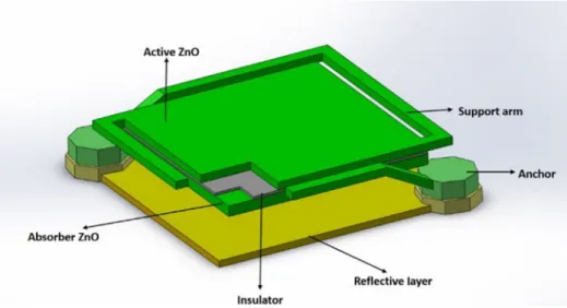
Fig. 1 Three-dimensional cross-sectional view of bilayer microbolometer.
Fig. 2 Simulation setup of (a) single-layer structure and (b) bilayer structure with ZnO layers grown at 120°C and 250°C (ZnO120and ZnO250).
Also, the absorption properties of 210-nm-thick proposed structure are calculated with respect to the incidence angle, which varies from 0 deg (normally incident) to 90 deg. Up to 60 deg, the average absorption is still more than 80% of its maximum value and after then it decreases rapidly (Fig.4). 3 Thermal Simulations
The parameters in Eq. (1) including the thermal conductance are required for NETD calculation. To simulate the thermal conductance of the microbolometers and evaluate the time constants, thermal simulations are performed using the Coventorware simulation software. The physical properties
of ZnO required for thermal simulations are taken as follow-ing: density is 5.6 g∕cm3,7specific heat is 40.25 J∕mol:K,8
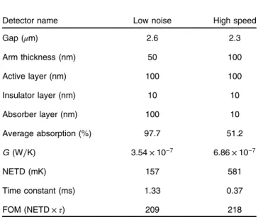
and thermal conductivity is 90 W∕m:K.9The thermal prop-erties of Al2O3are obtained from database of Coventorware software. All simulated structures have 35μm × 35 μm pixel area and 2-μm arm width. Support arms are connected to the active layer. Arm thickness of the detector is associated with the thermal conductance of the detector5and cannot exceed thickness of the active layer. Other properties required for NETD calculation are given in Table1.
Due to the trade-off between NETD and time constant, two types of detector designs are proposed: low noise and high speed. The structural details and performance values of both detectors are given in Table2. The ultimate NETD per-formance, 157 mK, are achieved with 210-nm total body thickness and 50-nm arm thickness. Time constant of the low-noise detector is evaluated as 1.33 ms and compatible with the frame rates up to 300 Hz.10 On the other hand, a high-speed detector is obtained with 120-nm total body thickness and 100-nm arm thickness. The high-speed detec-tor has 0.37-ms estimated time constant which is compatible with frame rate up to 900 Hz;10 however, it has a higher NETD value, 581 mK, compared to low-noise detector.
An optimized bilayer ZnO bolometer structure provides similar average absorption values with a much thinner body compared to a single-layer ZnO bolometer structure. Therefore, time constant decreases in bilayer case for similar NETD values due to lower thermal capacitance. In addition, Fig. 3 Simulation results. (a) Single-layer reference structures. (b) Bilayer proposed structures.
(c) Average absorption comparing single-layer (dashed bars) and bilayer structures.
NETD decreases in bilayer case for similar time constant val-ues due to higher average absorption. The comparison of bilayer and single layer ZnO results is given in Table3. It should be noted here that a possible increase in 1∕f noise due to thinner active layer is not considered in the calcula-tions, which can be solved by material development strategies.
It is important to see the simulated performance of all-ALD microbolometers in perspective with commercially available products because all-ALD detectors are promising to have disruptive low cost due to their simplified fabrication by single ALD growth. Although current market products provide <40 mK NETD performance, all-ALD detectors can be suitable for cost-effective applications. The compari-son of all-ALD simulated results and market products is shown in Fig.4.
In this paper, we also investigated the performance of ultrathin microbolometers (shown with filled triangles in Fig.5) to see the performance limits of all-ALD microbol-ometers. Yoneoka et al.13 fabricated ALD-metal uncooled
microbolometers with a body thickness less than 10 nm. Although ultrathin and suspended structures are not easy to fabricate, they represent the performance limits that can be obtained by bilayer ZnO structure. The performance of ultrathin microbolometers is given in Table4.
Ultrathin microbolometers promise very low NETD values and superior time constant performance. Despite manufacturing challenges, these results show that all-ALD Table 1 The detector parameters for NETD calculation.4
Parameter Value
Resistance 135 kΩ
Active detector area/fill factor 620 μm2∕50.5%
TCR −10.4%∕K DC responsivity 5.2 × 10⁵V∕W FPA size 384 × 288 Electrical bandwidth 5 kHz Detector noise 27 μVrms Transmission of optics 0.93
Table 2 The structural details and performance values of all-ALD microbolometers.
Detector name Low noise High speed
Gap (μm) 2.6 2.3 Arm thickness (nm) 50 100 Active layer (nm) 100 100 Insulator layer (nm) 10 10 Absorber layer (nm) 100 10 Average absorption (%) 97.7 51.2 G (W∕K) 3.54 × 10⁻⁷ 6.86 × 10⁻⁷ NETD (mK) 157 581 Time constant (ms) 1.33 0.37 FOM (NETD× τ) 209 218
Table 3 The performance comparison of all-ALD (bilayer ZnO) and all-ZnO (single layer) microbolometer by Kesim et al.4
Name NETD (mK) τ (ms) FOM (mK.ms)
Low noise 157 1.33 209
High speed 581 0.37 218
Detector 14 171 6.6 1129
Detector 24 940 0.32 301
Fig. 5 The performance comparison of commercially available prod-ucts11,12 and simulated detectors. ULIS sensors stated as having
<10 ms time constant.
Table 4 The structural details and performance values of ultrathin microbolometers. Ultrathin detectors 1 2 3 Gap (μm) 2.4 2.5 2.5 Arm thickness (nm) 10 10 10 Active layer (nm) 10 10 10 Insulator layer (nm) 10 10 10 Absorber layer (nm) 10 20 30 Average absorption (%) 29.3 47.6 61.4 G (nW∕K) 70.2 70.8 70.9 NETD (mK) 104 64 50 Time constant (ms) 1.07 1.33 1.57 FOM (NETD× τ) 111 86 79
technique can be a very attractive route to realize next-generation ultralow-cost and high-performance infrared imaging.
4 Conclusion
This paper presents an all-ZnO bilayer bolometer, operating in the LWIR regime, which can be fabricated simply by ALD. Absorptivity of the microbolometer can be increased more than 100% in comparison with the same thickness of single layer due to bilayer design of ZnO. Simulation results show that bilayer structures display better performance than single-layer structures in terms of NETD and time constant. Among the proposed structures, low-noise detector provides 157-mK NETD value and is also compatible with 300-Hz frame rate, and high speed detector provides 0.37-ms time constant, compatible with 900 Hz, with a relatively lower NETD performance of 581 mK.
Acknowledgments
K.G. and Z.S. thank TUBITAK-BIDEB for MS scholarships. Funding source: Scientific and Technological Research Council of Turkey (TUBITAK) (112M004, 112E052, 113M815, 114E645, 2228A, 2211).
References
1. M. Y. Tanrıkulu, “An uncooled infrared microbolometer detector array using surface micromachined MEMS technology,” PhD Thesis, Middle East Technical University, Department of Electrical and Electronics Engineering (2007).
2. A. Rogalski,“History of infrared detectors,”Opto-Electron. Rev.20, 279–308 (2012).
3. A. Rogalski and K. Chrzanowski,“Infrared devices and techniques (revision),”Metrol. Meas. Syst.21(4), 565–618 (2014).
4. Y. E. Kesim et al.,“An all-ZnO microbolometer for infrared imaging,” Infrared Phys. Technol.67, 245–249 (2014).
5. R. K. Bhan, C. R. Jalwaina, and S. K. Lomash,“Uncooled infrared microbolometer arrays and their characterisation techniques,” Def. Sci. J.59, 580–589 (2009).
6. E. Battal et al.,“Atomic-layer-deposited zinc oxide as tunable uncooled infrared microbolometer material,”Phys. Status Solidi A211, 2475– 2482 (2014).
7. R. C. Weast, M. J. Astle, and W. H. Beyer, CRC Handbook of Chemistry and Physics, 69th ed., CRC Press, Boca Raton, Florida (1988). 8. International Zinc Association,“Zinc oxide properties,” http://www.
zinc.org/zinc_oxide_properties(12 March 2017).
9. J. Alvarez-Quintana et al.,“Temperature dependent thermal conduc-tivity of polycrystalline ZnO films,”J. Appl. Phys.107, 063713 (2010). 10. B. Fièque et al.,“Uncooled microbolometer detector: recent
develop-ments at ULIS,”Infrared Phys. Technol.49, 187–191 (2007) 11. Semi Conductor Devices,“All uncooled products,”http://www.scd.co.il/
Templates/showpage.asp?DBID=1&LNGID=1&TMID=84&FID=1288 (12 March 2017).
12. ULIS,“Thermal imaging sensors,”http://www.ulis-ir.com/index.php? infrared-detector=products(12 March 2017).
13. S. Yoneoka et al.,“ALD-metal uncooled bolometer,” inProc. of the IEEE Int. Conf. on Micro Electro Mechanical Systems (IEEE‘11), pp. 676–679 (2011).
Muhammet Poyraz is a PhD student in electrical engineering at Stanford University and a graduate researcher at Canary Center at Stanford for Cancer Early Detection. He received his BS degree from Bilkent University, Turkey in electrical and electronics engineer-ing. He joined professor Utkan Demirci’s Lab at Stanford University in 2016 as a graduate student. He is currently working on plasmonic-based biosensing technologies for point of care applications. Kazim Gorgulu received his BS degree in 2015 from the Department of Electrical and Electronics Engineering at Bilkent University where he is currently an MS candidate. His research interests are photonics and nanoscience.
Zulkarneyn Sisman received his BS degree in electrical and elec-tronics engineering from Bilkent University in 2015. He is currently an MS candidate in the same department and also working as an electronic design engineer in Meteksan Defense.
Mahmud Yusuf Tanrikulu received his PhD in electrical and elec-tronics engineering with high honors from Middle East Technical University (METU), Ankara, in 2007. His PhD studies focused on the design and implementation of uncooled infrared microbolometer arrays. From 2007 to 2013 he worked as a scientific project specialist in METU-MEMS Center studying on the uncooled infrared detector projects. He is now an assistant professor in Department of Electrical-Electronics Engineering in Adana Science and Technology University.
Ali Kemal Okyay received his BS degree in electrical and electronics engineering from METU, in 2001 and his MS and PhD degrees in electrical engineering from Stanford University, CA, in 2003 and 2007, respectively. Since January 2008, he worked as a faculty member at Bilkent University, where he held joint appointments as an assistant professor in the electrical and electronics engineering department, and the Institute of Material Science and Nanotechnology.