Colorimetric and Near-Absolute Polarization-Insensitive
Refractive-Index Sensing in All-Dielectric Guided-Mode Resonance Based
Metasurface
Deniz Umut Yildirim,
*
,†,‡Amir Ghobadi,
†,‡Mahmut Can Soydan,
†,‡Murat Gokbayrak,
†Ahmet Toprak,
†Bayram Butun,
†and Ekmel Ozbay
*
,†,‡,¶,§†NANOTAM-Nanotechnology Research Center, ‡Department of Electrical and Electronics Engineering,¶Department of Physics,
and§UNAM-Institute of Materials Science and Nanotechnology, Bilkent University, 06800 Ankara, Turkey
*
S Supporting InformationABSTRACT: Colorimetric detection of target molecules with insensitivity to incident-light polarization has attracted considerable attention in recent years. This resulted from the ability to provide rapid output and reduced assay times as a result of color changes upon altering the environment that are easily distinguishable by the naked eye. In this paper, we propose a highly sensitive refractive-index sensor, utilizing the excitation of guided modes of a novel two-dimensional periodically modulated dielectric grating-waveguide structure. The optimized nanosensor can numerically excite guided-mode resonances with an ultranarrow linewidth (full width at half-maximum) of 0.58 nm. Sensitivity is numerically investigated by considering the deposition of dielectric layers
on the structure. For a layer thickness of 30 nm, the maximum sensitivity reached as high as 110 nm/refractive index unit (RIU), resulting in a very high figure of merit of 190. The fabricated devices with 30 nm aluminum oxide and zinc oxide coatings achieved a maximum sensitivity of 235.2 nm/RIU with a linewidth of 19 nm. Colorimetric detection with polarization insensitivity is confirmed practically by a simple optical microscope. Samples with different coatings have been observed to have clearly distinct colors, while the color of each sample is nearly identical upon azimuthal rotation. Excellent agreement is obtained between the numerical and experimental results regarding the spectral position of the resonances and sensitivity. The proposed device is, therefore, highly promising in efficient, highly sensitive, almost lossless, and compact molecular diagnostics in the field of biomedicine with personalized, label-free, early point-of-care diagnosis and field analysis, drug detection, and environmental monitoring.
B
iosensors play a vital role in improving the overall well-being of the society. The detection techniques used in biosensors can be broadly divided into free and label-based techniques.1 Traditional methods of label-based techniques enabled us to gain an improved understanding on many biological processes and cellular actions.2−7 However, using fluorescent dyes, radioactive labels, and staining agents essentially limit the scope of the experiment as they require prior knowledge of the target’s presence and the label may interfere with the process.8 Therefore, there has been significant effort made toward developing label-free biosensors that can allow any sample to be analyzed with minimal preparation and assay times.1 Over the last decade, label-free biosensing has made great improvements due to the develop-ments in nanotechnology.9Strong light−matter interactions in nanophotonic structures have shown high sensitivity, cost effectiveness, and practicality in many areas, such as biomedicine,10−16 drug detection,17 reaction monitoring,18 and environmental control.19,20 Among the label-free assays, colorimetric biosensing has, in particular, attracted muchattention because the rapid color change output upon changing the external environment can be read out in thefield, that is, at the point of care, by the naked eye. Therefore, this technology is not confined to the laboratory, it does not require expensive or advanced instrumentation, and the data readout can be carried out in wider clinical practice without requiring trained personnel.21−24 Insensitivity to incident-light polarization is also highly desirable as it would eliminate the requirement of polarizing equipment. In a practical setting, sensitivity to polarization would also mean that a sample reflects different colors depending on its azimuthal orientation with respect to the observer, when an arbitrarily polarized light is incident on it. A polarization-insensitive structure, on the other hand, would reflect the same color at all azimuthal orientations. Combining all of these, a colorimetric sensor with polarization Received: May 20, 2019
Revised: July 12, 2019 Published: July 15, 2019
Article
pubs.acs.org/JPCC Cite This:J. Phys. Chem. C 2019, 123, 19125−19134
insensitivity results in simpler instrumentation for interfacing, faster and more reliable readout with more self-contained devices of smaller footprints, and a lower cost.
In the broadfield of optical and label-free sensing, there are many competing technologies. Among these, sensors based on surface plasmon polaritons (SPPs) or localized surface plasmon r esonances (LSP Rs ) of met al lic stru c-tures10,12,14,15,17,18,20,25have seen the most extensive industrial adoption. Both methods can yield resonances in the visible range of the electromagnetic spectrum with polarization-insensitive unit cell arrangements and, therefore, enable colorimetric detection with high sensitivity. However, plasmonic sensing has inherently limited performance in terms of the resonance linewidth, which is broadened by the optical losses26,27due to free electrons and local heating.11,16 Localized heating may also alter the composition of analytes28 and prevent in vivo sensing. Moreover, metals are prone to oxidation and corrosion under high temperatures and harsh environments, which, in turn, limit their long-term perform-ance stability. On top of that, the excitation of SPPs requires p-polarized light, hence a polarizer, and phase-matching mechanisms, such as prisms,29resulting in sophisticated optics.
As a consequence, transparent dielectric nanoresonators stand out as strong candidates for not only biosensing but also for nanophotonics.30
All-dielectric nanophotonics is a rapidly developing field because the resonant nanostructures, such as silicon nano-particles, not only support electric-type (dipole, quadrupole, etc.) resonances, as in metallic nanoparticles, but also magnetic multipole Mie resonances,30−34with tailorable35 and actively tunable36,37 resonance features. Similar to their plasmonic counterparts, the spectral positions of these resonances also strongly depend on the properties of the dielectric environ-ment,38yet they can achieve higher quality-factors due to lower optical losses.30,39 These offer interesting opportunities for biosensing and refractive-index sensing. The present studies in this field mostly utilized silicon11,16,40−42 with sensitivities comparable to LSPR sensors. Although silicon has a negligible loss in the near-infrared region, its high refractive index in the visible region comes at a price of increased absorption due to interband transitions. Indeed, TiO2and GaP are shown to have better scattering efficiencies in the visible range,43 yet their application to colorimetric sensing without optical losses requires further research.
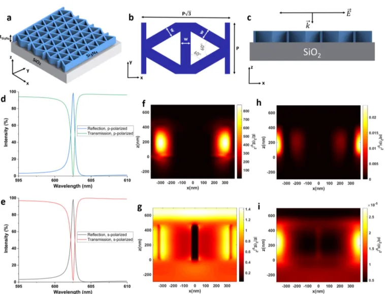
Figure 1.Proposed design and unit cell. (a) Device I to excite GMRs. (b) Unit cell of Device I, detailing the 2D grating, as seen from the top view. (c) Dielectric layers, as seen from the side view, and illumination by p-polarized plane wave. Transmission and reflection spectra for Device I (d) under p-polarized and (e) under s-polarized incident plane waves.|E|2/|E0|2 at the XZ plane during (f) on-resonance at 602.5 nm and (g)
off-resonance at 750 nm;|H|2at the XZ plane during (h) on-resonance and (i) off-resonance. |E|2and|H|2are the modulus of electric and magnetic fields inside Device I; |E0|2and|H0|2denote that of incident light. GWS extends from z = 0 to z = 460 nm.
Dielectric materials with negligible optical losses, when arranged periodically, can also show guided-mode resonance (GMR) phenomena.44−50 GMRs define the phase-matched coupling between the free-space radiation and a waveguide’s supported (guided) modes, and they have a leaky nature due to the periodicity of the structure.44−49,51 They result in resonances with narrow linewidth and high sensitivity to the changes in the surrounding medium’s refractive index, which are very well suited to colorimetric sensing applications52,53 with negligible optical losses. Sensitivity also benefits from utilizing a grating with sharp features, owing to the high localization of the electromagnetic fields around these regions.54 The problem with GMR-based devices that utilize one-dimensional (1D) gratings as their coupling element is sensitivity to incident-light polarization.49,55,56
In the present paper, we propose a novel design that utilizes a two-dimensional subwavelength grating-waveguide structure to excite its GMRs. We employ the finite-difference time-domain (FDTD) method to numerically show that the coupling of incident light to the GMRs yields perfect reflection of light (98.7%) with 0.58 nm of full width at half-maximum (FWHM) at 602.5 nm, under p-polarized incident light. In the literature, the refractive-index sensing performance is fre-quently evaluated by changing the refractive index of the entire environment.57−64We, however, investigated a scenario that is closer to biosensing by considering the deposition conformal dielectric layers (an example can be NH2 (amine) groups) coated over the device. The highest sensitivity reached as high as 110 nm/refractive index unit (RIU) for a biolayer thickness of 30 nm, yielding a very highfigure of merit (FoM) of 190. Moreover, the proposed device preserves perfect reflection of >98% at all source polarization angles as well as the spectral position of the resonance. We then transferred these numerical findings to the fabricated devices. The highly sensitive sensing of adsorbed layers and change of the surrounding refractive index are experimentally demonstrated by comparing a bare device and two devices with 30 nm alumina (Al2O3) and zinc oxide (ZnO) layers coated by atomic layer deposition (ALD). These proof-of-concept devices offered a high experimental sensitivity of 235.2 nm/RIU, with a resonance linewidth of 19 nm. Examination of samples with the naked eye showed that each sample with a different coating has a distinct color, owing to the high sensitivity and narrow linewidth. The samples also preserved the reflected color upon 90° of rotation, so insensitivity to incident-light polarization is also verified. Excellent agreement is obtained between the numerical and experimental results in terms of the spectral position of the resonances and sensitivity. The spectral tunability of the resonances is shown numerically by changing the key geometrical parameters of the device. We first elucidate the resonance mechanism in an optimized grating-substrate structure. We then demonstrate the polarization insensitivity and sensing performance of the device and scrutinize the effect of geometrical parameters on thefigure of merit of the device. Finally, we present the experimental results for the fabricated devices.
■
RESULTS AND DISCUSSIONExciting Guided-Mode Resonances of a Grating-Waveguide Structure with Polarization Insensitivity. Our proposed device in Figure 1a is designed to excite the guided modes of a unique two-dimensional, subwavelength, periodically modulated, high-refractive-index silicon nitride
(Si3N4) waveguide core. Due to the introduced periodicity in this structure, it additionally exhibits properties of a grating and essentially a phase-matching coupler element.44,49 This grating-waveguide structure (GWS) is supported by a quartz (SiO2) substrate. We call this design Device I. The
near-absolute polarization-insensitive hexagonal unit cell is based on our group’s previous study on ultra-narrowband perfect visible light absorption in monolayer graphene65 and wideband plasmonic light absorbers.66 Figure 1b illustrates the details of our novel 2D subwavelength grating from the top view. Two dielectric layers and the excitation conditions are shown from the side view inFigure 1c. The critical design parameters in determining the spectral position of GMRs are the thickness of the grating region tSi3N4, the periodicity P of the unit cell in the y direction, and the width of each grating stripe w.
To investigate the spectral response of Device I, we utilize finite-difference time-domain simulations. Details of the simulation setup are outlined in theExperimental Section.
First, we set the geometrical design parameters tSi3N4, P, and w to their optimum values of 460, 450, and 60 nm, respectively. We then looked at the amount of power that is reflected or transmitted from Device I to gain insight about the resonance excitation. The simulation result inFigure 1d shows a sharp guided-mode resonance manifesting itself as a peak in reflection (98.7%) and a dip in transmission at 602.5 nm. The absorption due to the dispersion of dielectrics is negligible but not zero, which is why reflection cannot fully reach 100%. The same simulation is also performed by changing incident-light polarization from p to s polarization (E-field is now polarized in the y direction), and the result is shown in Figure 1e. Comparing these figures, the most important observation is that the spectral position of the resonance and the reflection intensity at resonance are almost identical, owing to the unit cell. The physics governing the excitation the GMRs is explained in detail in theSupporting Information.
To discern the resonance behavior, we plotted the electric and magnetic field (E-field and H-field) profiles at two different wavelengths, namely, when Device I is off-resonant or on-resonant. We demonstrate a comparison of the fields for these two situations in Figure 1f−i. These figures clearly indicate a strong field enhancement and the localization of bothfields inside the GWS region. Both fields are enhanced close to 3 orders of magnitude with respect to the incident light. It is the strong field localization and the large optical energy stored in the waveguide core that are responsible for the very small linewidth of the GMR. The electric field and magneticfield profiles in Figure 1f,h, respectively, imply that the fundamental mode of the slab waveguide is excited. This is entirely expected because of the relatively small thickness of the waveguide core region with respect to the wavelength, tSi3N4/λ, as the excitation of higher-order modes of a waveguide requires larger core thickness.56,67
Another intriguing feature of GMRs is their Fano lineshape. It emerges because of the interaction between the sharp resonance channel and the broad radiation continuum.68The subwavelength nature of the grating results in only zeroth-order diffracted wave to propagate, while all other diffracted orders are evanescent. Therefore, the incident wave is coupled evanescently to the guided mode.
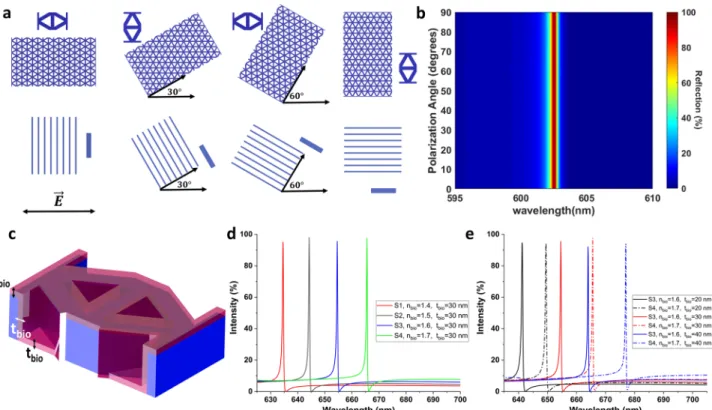
We now concentrate on the polarization insensitivity of Device I. We explained the reasoning behind using the hexagonal 2D unit cell to achieve polarization insensitivity
explicitly in our early works.65,66 Briefly, the idea behind achieving polarization insensitivity is to come up with a unit cell whose interaction with the incoming E-field changes as little as possible for all polarization angles. This is equivalent to stating that the E-field with a fixed polarization angle has to “observe” the same unit cell upon rotating the latter arbitrarily. By doing so form birefringence,69and the different excitation conditions between the TE and TM Bloch modes defined by the periodicity of the structure56are minimized, which are the main reasons why 1D gratings are polarization-sensitive.
To compare the unit-cell Device I with the devices using 1D grating, we kept the polarization angle of the incident wave at ϕ= 0° and rotated both unit cells for 0, 30, 60, and 90°. The result of this comparison is shown inFigure 2a. FromFigure 2a, it can be seen that our hexagonal unit cell has 60° of rotational symmetry, while the 1D grating has different unit cells for all polarization angles. The hexagonal unit cell is in different orientations for the 0 (60°) and 30° (90°) cases, but the interaction of the E-field with the unit cells is nearly identical (see the Supporting Information of ref65for a more detailed discussion). We examined the polarization insensi-tivity of Device I in more detail by sweeping the polarization angle of the source from 0 to 90°. The result in Figure 2b clearly demonstrates that Device I preserves almost constant reflection at a nearly fixed spectral position.
Refractive-Index Sensing with the Proposed Device. Our discussion of the guided-mode excitation and its theoretical treatment in the Supporting Information also points out the fact that the propagation constant of the guided mode β and therefore neff strongly depend on the refractive
indexes of the GWS and the superstrate regions. To analyze this, we consider a scenario where an aqueous or gaseous
solution containing target analytes is delivered over Device I with the help of a microfluidic channel. The accumulation of the target analytes on the surface will change the refractive indexes nsuper and nw, where the latter can be thought as a weighted average of nSi3N4and the background refractive index.
Since β is a constant under fixed grating periodicity, the resonance wavelength is shifted, fromeq S5. This wavelength shift can be directly related to the addition of the biolayers, and Device I can be calibrated differently for different relevant molecules. The small changes in the properties of the dielectric medium can be read if the sensor has large sensitivity values.
The shift of the resonance wavelength is usually quantified in the literature by altering the entire refractive index of the simulation region.57−64The possible downside of this method, however, is that the target molecules are typically confined to a very thin region that may be smaller than the decay length of the guided mode in the superstrate. In such a case, the optical fields are not decayed to negligible values in the air region above the biolayer. Therefore, if the biolayer refractive index is assigned to the entire superstrate region, including air, these opticalfields now interact with nbio, instead of air, and shift the GMRs considerably. As a result, the interaction of the optical fields with the superstrate is overestimated compared to its actual (air on top a thin biolayer) case. This causes the shift of GMRs to be significantly larger than their true values. Consequently,the accumulation of target analytes can be analyzed better by regarding them as a thin deposition layer on the GWS and treating sensitivity as a function of biolayer thickness. Only if the biolayer thickness is much thicker than the decay length of the guided mode can nbiobe safely assigned
to the entire simulation region.
Figure 2.Achieving near-absolute polarization-insensitive refractive-index sensing in Device I with the 2D grating. (a) Comparison of the unit cells of Device I and the design incorporating 1D grating under different rotations. (b) Reflection map of Device I for the polarization angles spanning from 0 (p, TM-polarization) to 90° (s, TE-polarization). (c) Device II with the adsorbed biolayer. Spectral shift of the guided-mode resonance depending on the (d) refractive index nbioand (e) thickness tbioof the biolayer.
To measure the sensitivity of Device I, we modeled the biolayer as a dielectricfilm, deposited as a conformal layer over Device 1. Device I with the attached biolayer is called Device II, which is shown inFigure 2c.
To evaluate sensing, we initiallyfixed the biolayer thickness tbioas 30 nm while varying its refractive index nbio. The shift of
the GMR peak in Device II is presented inFigure 2d. By taking the largest spectral shift of the GMR Δλ, the maximum sensitivity57−64(Smax) of Device II is found as Smax=Δλ/Δn =
(665.53 nm− 654.55 nm)/(1.7 − 1.6) = 110 nm/RIU. Based onFigure 2d, Smaxis obtained between S4 and S3 cases, that is, between nbio= 1.6 and nbio= 1.7. For our proposed device, it is observed that, as the biolayer refractive index gets larger, it becomes more sensitive. This is expected because of the following reason. Under thefixed fill factor of GWS with Si3N4,
the biolayer with a larger refractive index has a higher influence on nw, nsuper, and consequently neff, even if it has a constant
thickness.
To examine how changing biolayer thickness tbioaffects the performance of Device II, we considered S3 and S4 cases, and the results are shown inFigure 2e. Two important observations can be made from Figure 2e. First, as tbio is increased, the
GMRs continue to shift for constant nbiodue to the increased
interaction of opticalfields with the biolayer. At the same time, as the biolayer gets thicker, the GMRs shift more for the same Δn value of 0.1. This is because a thicker biolayer has a greater fill factor and again a higher influence on nw, so Device II
becomes more sensitive and can have larger Smaxvalues when a
thicker biolayer are attached on it.
With a calculated sensitivity (S) value of 110 nm/RIU and an FWHM of 0.58 nm, the figure of merit of our sensor reached as high as FoM = S/FWHM = 190. We also observed that the resonances get narrower as the biolayer refractive
index is increased. This is also expected by the coupled mode theory,44which found that the linewidth is proportional to the difference between the dielectric permittivities of the grating material and the surrounding mediumΔϵ.
We close this subsection by pointing out that the attachment of biological analytes may also change the geometrical dimensions that may shift the resonance frequency. Therefore, biosensing is realizable by Device I in addition to refractive-index sensing as outlined up to now. To point out an important design consideration, however, in refractive-index sensing, the overlap of the electromagnetic mode outside the guiding layer should be maximized to resolve all of the changes in the superstrate. Conversely, in biosensing, this overlap should only cover the ultrathin layer that the analytes attach to.11,70As another possible application, the biolayer thickness dependent shift of the resonance wavelength, under constant nbio, implies that this shift can be measured as a function of time to quantify the binding kinetics. These applications are an ongoing study at the present time.
Technological Tolerances of the Proposed Device and Effect of Geometrical Parameters on GMR Proper-ties and Sensing Performance. The results and discussion up to now have demonstrated that GMRs can be excited when the phase-matching condition is satisfied; that is, one of the evanescent diffracted order can be coupled to one of the guided waveguide modes. Although the waveguiding effects on the Bloch modes49of the periodically patterned waveguides are complicated, we can still have a solid understanding on how the spectral position of GMRs and the sensing properties of Device I and Device II depend on the structural parameters tSi3N4, P, and w.
To start with the spectral position of GMRs,eqs S5, S6, and S7 show that it strongly depends on the effective refractive Figure 3.Dependence of the reflection spectrum and the refractive-index sensing properties of Device I on the structural parameters. Reflection spectrum of Device I under varying (a) grating thickness tSi3N4, (c) unit cell periodicity in the y direction P, and (e) width of each stripe w. When
changing one parameter, we kept the other parameters at their optimum value. FWHM, sensitivity, and FoM of Device II when (b) tSi3N4, (d) P, and
(f) w are changed. FWHM is measured for Device I without the biolayer attachment, while sensitivity is measured for Device II by comparing the S3 and S4 cases, with tbio= 30 nm. In the unit cell periodicity sweeps, the width of grating is kept as w
P
2 15
= . All results are taken with the p-polarized incident wave.
index neff of the guided mode if we regard GWS as an asymmetric dielectric slab waveguide. This is done by considering the GWS as a medium with an effective dielectric permittivity.56,71 For the linewidth of the resonance, one can resort to the coupled mode theory, a multiple-interference model based on the geometrical ray picture, or the quality factor (Q factor) of a standard waveguide.44−46 For our analysis, we will employ the findings of the coupled mode theory,44which states that, in addition toΔϵ, the linewidth is proportional to the thickness of the grating tSi3N4but inversely
proportional to the propagation constant of guided mode β. The sensitivity, especially when the biolayer is a very thin layer, depends on the spatial extent of the mode and its overlap with the biolayer.11,70 This is controlled by the evanescent decay length of the guided mode in the superstrate region and thus neffagain.
Equations S6 and S7 clearly show that neff is determined primarily by normalized core thickness tSi3N4/λ and its average
refractive index nw. Significantly, the modes with higher β and
neffare confined more tightly to the core, and the optical fields
have smaller evanescent decay lengths in the substrate and superstrate regions. This has two critical implications. First, this smaller decay length associated with larger neff results in the less overlap of opticalfields with the adsorbed layer and poorer sensing performance. Second, the linewidth is reduced because of increasing β. This highlights the fundamental tradeoff between the two key parameters defining the performance of a sensor, namely, linewidth and sensitivity. While a small linewidth requires a guided mode with a large Q factor and hence large β, sensitivity necessitates a strong interaction of the opticalfield with the superstrate medium and thus a mode with looser confinement, larger leakage, and smaller neff. With this treatment of Device I and Device II, we
will now explain the dependence of the abovementioned features on the physical dimensions.
InFigure 3a, we show how the thickness of Si3N4GWS tSi3N4
affects the spectral response of Device I. The thickness of the waveguide core has a strong influence on neff, as shown ineqs.
S6 and S7, so it also has a large impact on the spectral position of resonance under afixed grating period, as ineq S5. It is clear from Figure 3a that the spectral position of GMR changes almost linearly with tSi3N4. This makes the GMRs easily tunable
to the application-at-hand but also prone to fabrication inaccuracies. In addition, as tSi3N4is increased, neffincreases
56,65
as well as the Q factor of the guided mode,44 so we see a decrease in the linewidth. Indeed, inFigure 3b, we plotted the variation of Device II’s sensing parameters with the thickness of GWS, and the linewidth steadily decreases, as tSi3N4increases.
However, the sensitivity of the sensor suffers due to the smaller interaction of the guided mode with the biolayer. Nevertheless, as tSi3N4 increases, the decrease in FWHM outweighs the
decrease in sensitivity, so FoM improves. However, increasing this thickness too much may obstruct or prevent the fabrication of the design because it may prevent the lift-off process or if the device is to be fabricated with etching, the long exposure time to the etchant would also make the sharp features rounded,72and the electromagnetic hotspots may be lost. Decreasing the thickness too much, on the other hand, may result in the cutoff of the mode.
The next parameter that we modified is the periodicity P of the unit cell. The reflection map shown inFigure 3c indicates
that the resonance wavelength changes linearly with the unit cell periodicity, but the effect on neff is opposite to that of
tSi3N4.To illustrate, while increasing tSi3N4underfixed P increases
neff, increasing the periodicity underfixed tSi3N4decreasesβ and neff, fromeq S3. Its effect on the sensing parameters is plotted
inFigure 3d, and they are in agreement with our reasoning by neff. Device II with a larger unit cell period has large sensitivity
and large bandwidth due to a more loosely confined mode, while the opposite is true for small periodicity. As the period gets smaller, the figure of merit is again dictated by the decrease in the linewidth as opposed to the decrease in the sensitivity. Lastly, the linear dependence of the resonance position on the periodicity gives Device I great tunability but also sensitivity to fabrication imprecisions. Decreasing the periodicity too much can give Device II a very large FoM at the cost of a more strenuous electron beam lithography step while fabricating the grating. Increasing the periodicity too much may cause GMR to disappear due to decreasedβ and neff, from
eq S5.
Finally, we examined the effect of the width of each stripe w of the 2D GWS and obtained the reflection map inFigure 3e. We divide our analysis into two in this section: w above 60 nm and w below 60 nm. For the former, we observed that, as w is increased beyond the mode cutoff, it causes the red shift of the resonance wavelength. Additional higher-order modes also start coupling to the waveguide, as it is increased even further. All of these can be explained by considering thefill factor of the grating material, and the resultant average refractive index of the GWS.49,56Increasing w increases thefill factor of Si3N4 with respect to the superstrate, so the GWS assumes a larger average refractive index nw. Based on the asymmetric dielectric
slab waveguide theory,56,67 this allows the waveguide to support more modes and increases the effective mode index neff
of existing modes. Therefore,eq S5requires the red shifting of resonance wavelength because β is a constant under the constant grating period P. The increased mode confinement causes a decrease in the linewidth, as shown in the right-half portion of Figure 3f. For the sensitivity, increasing the width too much is very detrimental because not only thefill factor of the superstrate material and thereby its weight in nwdecrease
but also the spatial overlap of the guided mode with the superstrate reduces. The decrease in sensitivity with increased w is clearly visible in the right-half portion ofFigure 3f. This region offers an interesting possibility for sensing, however. Instead of measuring the wavelength of a single GMR, one can look at the difference of the spectral positions of two resonances. This would eliminate the effect of noise sources, as their effect is common in both modes.
When w is too small, the guided mode proceeds toward the mode cutoff, and it eventually cannot be supported anymore, as the bottom portion of Figure 3e shows. Interestingly, however, this region offers a very small linewidth, although the mode is loosely confined to the core. This can be understood by considering the limiting case where GWS acts as a grating, but nw of the waveguide is exactly equal to the larger one of
nsuper and nsub. In such a case, the linewidth tends to go to
zero.73 The small width of each stripe also means that the weight of the background material will be very prominent on nw and the sensitivity will be greatly improved. Both small
bandwidth and large sensitivity promise ultrahigh FoM as the left-half portion of Figure 3f shows. Although this region appears ideal for refractive-index sensing, it also has the largest
intolerances to the fabrication errors because slightflaws can cause losing the entire GMR phenomenon.
To wrap up, the geometrical parameters should be determined based on the main requirement of the application-at-hand, that is, whether a small linewidth or large sensitivity is desired, because improving one tends to diminish the other. For the figure of merit, it should be remembered that targeting small FWHM outweighs targeting large sensitivity. In general, a device that is more tolerant to fabrication inaccuracies will offer more sensitivity instead of a small linewidth.
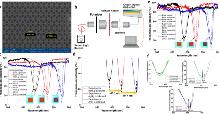
Fabrication and Characterization of the Proposed Guided-Mode Resonance Based Nanosensor. The numerical results up to now have demonstrated that colorimetric and near-absolute polarization-insensitive sensing of the changes in the refractive index of the surrounding medium is possible in a lossless, all-dielectric nanosensor, owing to the excitation of guided-mode resonances. As a proof of concept, we fabricated the proposed device with the procedure outlined in theExperimental Section. To investigate refractive-index sensing, the bare sample is compared with two other samples on which 30 nm of Al2O3and ZnO are coated with ALD. ALD is preferred because it best imitates the attachment of target analytes by producing uniform, conformal, and pinhole-free layers with very high thickness precision.
Figure 4a shows the top-view scanning electron microscopy (SEM) image of the patterned, bare nanosensor. In fabricating the proposed device, P is set constant at 460 nm, while w is chosen as 100 nm, in an effort to increase the tolerance to the fabrication inaccuracies. tSi3N4is chosen as 150 nm in order not to excite higher-order modes of the waveguide. Infinding the
transmission spectrum, a custom-made optical setup, whose details are given in theExperimental Section, was used.Figure 4b shows the schematic diagram of the optical setup. The slight adjustments we have made in the FDTD simulation setup to better model the experimental conditions are outlined in theExperimental Section.
In our initial set of experiments, we characterized the bare, alumina-coated, and ZnO-coated samples under p-polarized light. The experimental transmission spectra for these devices, compared with their corresponding FDTD simulations, are given in Figure 4c. The results in Figure 4c show that the resonance positions of all the samples are in good agreement with the numerical results, but the experimentally measured resonances are broadened and have larger dip magnitudes. This is primarily because of the following: in the FDTD simulations, we utilized perfect and infinite periodicity of a unit cell, imported from Figure 4a. In reality, however, there are slight variations between the individual hexagonal unit cells, and the number of them isfinite. These perturbations, that is, deviations from ideal conditions, contribute to more leakage of the guided mode, which in turn broadens and weakens the resonance. Similar to our discussion in the numerical part, the linewidth is observed to be the narrowest when Δϵ is the smallest. Indeed, the best FWHM is observed for ZnO-coated samples, and it is 22.1 nm. As aforementioned, the position of the resonances and their shift with changing background are mainly controlled by thefill factor of the grating material, and there is perfect agreement with the numerical and experimental results. The shift of resonances is investigated further in detail inFigure 4d to determine the sensitivity. The resonance shifts between larger nbio materials (Al2O3and ZnO) are higher, as also observed in the numerical analysis. The maximum Figure 4.Fabrication and optical characterization of the proposed nanosensor. (a) Top-view SEM micrograph of the fabricated bare device. (b) Schematic diagram of the optical characterization setup. (c) Experimental transmission spectra for the bare, Al2O3-coated, and ZnO-coated devices
under p-polarized incident light. (d) Shift of the excited GMRs. (e) Experimental transmission spectra for the bare, Al2O3-coated, and ZnO-coated
devices under s-polarized incident light. (f) Insensitivity of fabricated devices to incident-light polarization by comparing the excitation wavelengths of GMRs under p- and s-polarized light for each device. In panels (c) and (e), the spectrum of each device is connected to their associated optical microscope image.
experimental sensitivity of our proposed all-dielectric nano-sensor is recorded as Smax = Δλ/Δn = 49.5 nm/(1.983 −
1.778) = 241 nm/RIU, which is comparable to its plasmonic counterparts. Next, we performed the same set of experiments with s-polarized light, and the experimental results are plotted inFigure 4e. The results and discussion are similar to the p-polarization case. In the s-p-polarization case, however, the resonances all have smaller linewidths and smaller dip values. The smallest linewidth is reached as low as 19 nm, while the maximum sensitivity is measured as Smax = 235.2 nm/RIU.
Similar to the previous numerical results, the decrease in the linewidth predominates the decrease in sensitivity. The satisfactory experimentalfigure of merits of 10.9 and 12.3 are obtained for p-polarized and s-polarized incident radiation, respectively.
For practical settings, the observation of the samples with the naked eye is of paramount importance. In our observed nanosensor devices, we observed clearly distinguishable color differences between different samples (of only 30 nm adsorbed layer), as in Figure 4c,e, by merely using a simple optical microscope. The nearly identical color of the samples is an indication of insensitivity to the polarization of incident light, which is verified quantitatively by comparing the transmission spectra of the samples under p- and s-polarized incident light. The results are demonstrated inFigure 4f where it can be seen that the bare samples have nearly the same resonance position, whereas for the coated samples, the difference between peak positions is only 2 nm. As a result, colorimetric and near-absolute polarization insensitive detection of ultrathin layers of adsorbed molecules is verified by using minimal instrumenta-tion. This makes our proposed device highly applicable to point-of-care personal diagnostics andfield analyses.
■
CONCLUSIONSIn conclusion, in this paper, we analyzed and experimentally confirmed the highly sensitive measurement of adsorbed layers and the change of the surrounding medium’s refractive index numerically. Colorimetric detection and near-absolute insensi-tivity of the proposed design to the polarization incident light are verified. Our novel 2D subwavelength periodically modulated grating structure also acts as a waveguide to support the guided modes. The interaction of absorbed layers with the guided mode within the evanescent decay length of the mode results in the shift of the resonance wavelength. Numerically calculated linewidth of the resonance of 0.58 nm and a maximum sensitivity of 110 nm/RIU resulted in a very highfigure of merit of 190. A design that is more tolerant to fabrication inaccuracies is fabricated, and the maximum sensitivity reached as high as 235.2 nm/RIU while the linewidth is measured as 19 nm. Perfect agreement of resonance positions and their shift is obtained between experimental results and numerical simulations. The perform-ance of our nanosensor can be improved even further and/or adapted to different scenarios by the physical laws and explanations outlined in this paper, at the cost of a more cumbersome fabrication route. Overall, our simple yet robust and easy-to-fabricate device holds great promise in many areas such as biomedicine with less invasive and point-of-care therapies, drug detection, and contamination control.
■
EXPERIMENTAL SECTIONFabrication of the Nanosensor Device. For the fabrication of the samples, first, a typical commercial square-shaped quartz substrate with 144 mm2area was cleaned with acetone, isopropanol (IPA), and deionized water and then was dried with N2flow, to be used as a substrate. The surface was further treated using oxygen plasma for 5 min before starting the deposition of thinfilms. First, a 150 nm thick Si3N4layer
was coated by using a plasma-enhanced chemical vapor deposition system (SAMCO). This process was carried out with SiH4, NH3, and N2flow rates of 160, 6, and 500 sccm,
respectively, at a temperature of 275°C, RF power of 130 W, and pressure of 75 Pa. Electron beam lithography (RAITH E-Line Plus) was employed to fabricate the hexagonal grating unit cell, with the ZEP520A resist. Electron beam exposure was then performed with a beam writer at an accelerating voltage of 30 kV, aperture size of 7μm, working distance of 6 mm, and beam current of 22 pA. To obtain our desired dimensions, we used an exposure dose of 60μC/cm2. After the exposure, the samples were developed at room temperature by utilizing xylene solution for 4 min followed by immersion in IPA for 30 s. Then inductively coupled plasma reactive-ion etching was performed (SAMCO) with the following etching conditions: flow rates of SF6and argon at 4 and 20 sccm, respectively, and
at an RF power of 10 W and pressure of 0.6 Pa. The ZEP resist was subsequently stripped by an ultrasonic bath in NMP at 50 for 15 min.Figure 4a shows the hexagonal grating pattern with P = 460 nm and w = 100 nm.
Optical Characterization. A custom-made optical setup was used for the transmission measurements of the samples. The setup comprised a spectrometer (OceanOptics-USB4000), a personal computer (PC), and a xenon light source (Spectral Products ASB-XE-175). Light was transmitted by a multimode optical fiber to a lens that illuminates the nanosensor through a collimating lens. In between this lens and the input, the light was polarized by a mounted linear polarizer with indexed rotation (Thorlabs RPS1X15). Colli-mated and polarized light was focused onto the sample by a focusing lens, then transmitted through the biosensor, and collected by the imaging lens. The image was projected onto an aperture that enables only the signal from the selected region of the sample being measured to be transmitted. Another focusing lens coupled this signal to the collection fiber. The spectrum was then measured by the spectrometer. The dispersion effect of the dielectric layers mentioned in this paper was determined by a J.A. Woollam Co. Inc. V-VASE ellipsometer, and they were in good agreement with the models based on the Sellmeier equation.74 These optical constants were input to the numerical simulations.
Numerical Simulations. In the FDTD simulations, we illuminated the unit cell with a broadband plane-wave at normal incidence whose electric field is polarized in the x direction (ϕ = 0, p-polarization), as inFigure 1c. In the x and y directions of the simulation region, we used periodic boundary conditions, while in the z direction perfectly matched layers were adopted and they were placed 4 wavelengths away from the structure. We used two monitors that are an adequate distance away from the structure tofind the reflected (R) and transmitted (T) power, normalized to the incident power. In simulating the fabricated devices, all of the FDTD simulations were performed by importing the SEM image of the structure in Figure 4a to the Lumerical FDTD solver software75 and
defining it as the top layer. The biolayer was defined as shown inFigure 2c with a biolayer thickness tbioof 30 nm. All of the
structures were modeled with rounded top edges and a radius of curvature of 10 nm.
■
ASSOCIATED CONTENT*
S Supporting InformationThe Supporting Information is available free of charge on the
ACS Publications websiteat DOI:10.1021/acs.jpcc.9b04748. Physical insight on the excitation of guided-mode resonances and their analytical analysis based on the dielectric slab waveguide formulas and grating equations (PDF) (ZIP)
■
AUTHOR INFORMATIONCorresponding Authors
*E-mail:[email protected] (D.U.Y.). *E-mail:[email protected] (E.O.).
ORCID
Deniz Umut Yildirim: 0000-0002-2160-1142
Notes
The authors declare no competingfinancial interest.
■
ACKNOWLEDGMENTSAuthors acknowledgefinancial support from the Scientific and Technological Research Council of Turkey (TUBITAK) and DPT-HAMIT under Project Nos. 113E331, 114E374, and 115F560. One of the authors (E.O.) also acknowledges partial support from the Turkish Academy of Sciences (TUBA).
■
REFERENCES(1) Sang, S.; Wang, Y.; Feng, Q.; Wei, Y.; Ji, J.; Zhang, W. Progress of new label-free techniques for biosensors: A review. Critical Reviews in Biotechnology 2016, 36, 1−17.
(2) Elf, J.; Li, G. W.; Xie, X. S. Probing transcription factor dynamics at the single- molecule level in a living cell. Science 2007, 316, 1191− 1194.
(3) Schuler, B.; Lipman, E. A.; Eaton, W. A. Probing the free-energy surface for protein folding with single-molecule fluorescence spec-troscopy. Nature 2002, 419, 743−7.
(4) Sako, Y.; Minoghchi, S.; Yanagida, T. Single-molecule imaging of EGFR signalling on the surface of living cells. Nat. Cell Biol. 2000, 2, 168−172.
(5) Jaiswal, J. K.; Simon, S. M. Imaging single events at the cell membrane. Nat. Chem. Biol. 2007, 3, 92−98.
(6) Lang, M. J.; Fordyce, P. M.; Fordyce, A. M.; Neuman, K. C.; Block, S. M. Simultaneous, coincident optical trapping and single-molecule fluorescence. Nat. Methods 2004, 1, 133−139.
(7) Huang, B.; Wu, H.; Bhaya, D.; Grossman, A.; Granier, S.; Kobilka, B. K.; Zare, R. N. Counting low-copy number proteins in a single cell. Science 2007, 315, 81−84.
(8) Armani, A. M.; Kulkarni, R. P.; Fraser, S. E.; Flagan, R. C.; Vahala, K. J. Label-free, single-molecule detection with optical microcavities. Science 2007, 317, 783−787.
(9) Rosi, N. L.; Mirkin, C. A. Nanostructures in Biodiagnostics. Chem. Rev. 2005, 105, 1547−1562.
(10) Lim, W. Q.; Gao, Z. Plasmonic nanoparticles in biomedicine. Nano Today 2016, 11, 168−188.
(11) Bontempi, N.; Chong, K. E.; Orton, H. W.; Staude, I.; Choi, D. Y.; Alessandri, I.; Kivshar, Y. S.; Neshev, D. N. Highly sensitive biosensors based on all-dielectric nanoresonators. Nanoscale 2017, 9, 4972−4980.
(12) Howes, P. D.; Rana, S.; Stevens, M. M. Plasmonic nanomaterials for biodiagnostics. Chem. Soc. Rev. 2014, 43, 3835− 3853.
(13) Song, Y.; Huang, Y. Y.; Liu, X.; Zhang, X.; Ferrari, M.; Qin, L. Point-of-care technologies for molecular diagnostics using a drop of blood. Trends Biotechnol. 2014, 32, 132−139.
(14) Joshi, G. K.; Deitz-Mcelyea, S.; Johnson, M.; Mali, S.; Korc, M.; Sardar, R. Highly specific plasmonic biosensors for ultrasensitive MicroRNA detection in plasma from pancreatic cancer patients. Nano Lett. 2014, 14, 6955−6963.
(15) Saha, K.; Agasti, S. S.; Kim, C.; Li, X.; Rotello, V. M. Gold Nanoparticles in Chemical and Biological Sensing. Chem. Rev. 2012, 112, 2739−2779.
(16) Yavas, O.; Svedendahl, M.; Dobosz, P.; Sanz, V.; Quidant, R. On-a-chip Biosensing Based on All-Dielectric Nanoresonators. Nano Lett. 2017, 17, 4421−4426.
(17) Zhang, J.; Wang, L.; Pan, D.; Song, S.; Boey, F. Y.; Zhang, H.; Fan, C. Visual cocaine detection with gold nanoparticles and rationally engineered aptamer structures. Small 2008, 4, 1196−1200. (18) Shi, L.; Jing, C.; Ma, W.; Li, D. W.; Halls, J. E.; Marken, F.; Long, Y. T. Plasmon resonance scattering spectroscopy at the single-nanoparticle level: Real-time monitoring of a click reaction. Angew. Chem., Int. Ed. 2013, 52, 6011−6014.
(19) Long, F.; Zhu, A.; Shi, H. Recent advances in optical biosensors for environmental monitoring and early warning. Sensors 2013, 13, 13928−13948.
(20) Chen, L.; Fu, X.; Lu, W.; Chen, L. Highly sensitive and selective colorimetric sensing of Hg 2+ based on the morphology transition of silver nanoprisms. ACS Appl. Mater. Interfaces 2012, 5, 284−290.
(21) Aldewachi, H.; Chalati, T.; Woodroofe, M. N.; Bricklebank, N.; Sharrack, B.; Gardiner, P. Gold nanoparticle-based colorimetric biosensors. Nanoscale 2018, 10, 18−33.
(22) Song, Y.; Wei, W.; Qu, X. Colorimetric biosensing using smart materials. Adv. Mater. 2011, 23, 4215−4236.
(23) Verma, M. S.; Rogowski, J. L.; Jones, L.; Gu, F. X. Colorimetric biosensing of pathogens using gold nanoparticles. Biotechnol. Adv. 2015, 33, 666−680.
(24) Tang, L.; Li, J. Plasmon-based colorimetric nanosensors for ultrasensitive molecular diagnostics. ACS Sens. 2017, 2, 857−875.
(25) Homola, J. Surface plasmon resonance sensors for detection of chemical and biological species. Chem. Rev. 2008, 108, 462−493.
(26) Yildirim, D. U.; Ghobadi, A.; Soydan, M. C.; Atesal, O.; Toprak, A.; Caliskan, M. D.; Ozbay, E. Disordered and Densely Packed ITO Nanorods as an Excellent Lithography- Free Optical Solar Reflector Metasurface. ACS Photonics 2019, 1812.
(27) Soydan, M. C.; Ghobadi, A.; Yildirim, D. U.; Erturk, V. B.; Ozbay, E. All Ceramic- Based Metal-Free Ultra-broadband Perfect Absorber. Plasmonics 2019,DOI: 10.1007/s11468-019-00976-z.
(28) Mahmoudi, M.; Lohse, S. E.; Murphy, C. J.; Fathizadeh, A.; Montazeri, A.; Suslick, K. S. Variation of protein corona composition of gold nanoparticles following plasmonic heating. Nano Lett. 2013, 14, 6−12.
(29) Maier, S. A. Plasmonics: Fundamentals and Applications; Springer Science & Business Media: 2007; pp 1−223.
(30) Kuznetsov, A. I.; Miroshnichenko, A. E.; Brongersma, M. L.; Kivshar, Y. S.; Luk’yanchuk, B. Optically resonant dielectric nanostructures. Science 2016, 354, aag2472.
(31) Kuznetsov, A. I.; Miroshnichenko, A. E.; Fu, Y. H.; Zhang, J.; Lukyanchukl, B. Magnetic light. Sci. Rep. 2012, 2, 492.
(32) Evlyukhin, A. B.; Reinhardt, C.; Seidel, A.; Luk’Yanchuk, B. S.; Chichkov, B. N. Optical response features of Si-nanoparticle arrays. Phys. Rev. B 2010, 82, 045404.
(33) van de Haar, M. A.; van de Groep, J.; Brenny, B. J.; Polman, A. Controlling magnetic and electric dipole modes in hollow silicon nanocylinders. Opt. Express 2016, 24, 2047.
(34) Shi, L.; Harris, J. T.; Fenollosa, R.; Rodriguez, I.; Lu, X.; Korgel, B. A.; Meseguer, F. Monodisperse silicon nanocavities and photonic
crystals with magnetic response in the optical region. Nat. Commun. 2013, 4, 1904.
(35) Staude, I.; Miroshnichenko, A. E.; Decker, M.; Fofang, N. T.; Liu, S.; Gonzales, E.; Dominguez, J.; Luk, T. S.; Neshev, D. N.; Brener, I.; et al. Tailoring directional Scattering through magnetic and electric resonances in subwavelength silicon nanodisks. ACS Nano 2013, 7, 7824−7832.
(36) Parry, M.; Komar, A.; Hopkins, B.; Campione, S.; Liu, S.; Miroshnichenko, A. E.; Nogan, J.; Sinclair, M. B.; Brener, I.; Neshev, D. N. Active tuning of high-Q dielectric metasurfaces. Appl. Phys. Lett. 2017, 111, 053102.
(37) Sautter, J.; Staude, I.; Decker, M.; Rusak, E.; Neshev, D. N.; Brener, I.; Kivshar, Y. S. Active tuning of all-dielectric metasurfaces. ACS Nano 2015, 9, 4308−4315.
(38) Bohren, C. F.; Huffman, D. R. Absorption and Scattering of Light by Small Particles; Wiley Science Series; Wiley, 2008.
(39) Decker, M.; Staude, I. Resonant dielectric nanostructures: A low-loss platform for functional nanophotonics. J. Opt. (Bristol, U. K.) 2016, 18, 103001.
(40) Yan, J.; Liu, P.; Lin, Z.; Yang, G. New type high-index dielectric nanosensors based on the scattering intensity shift. Nanoscale 2016, 8, 5996−6007.
(41) Zhang, J.; Liu, W.; Zhu, Z.; Yuan, X.; Qin, S. Strong field enhancement and light-matter interactions with all-dielectric meta-materials based on split bar resonators. Opt. Express 2014, 22, 30889. (42) Yang, Y.; Kravchenko, I. I.; Briggs, D. P.; Valentine, J. All-dielectric metasurface analogue of electromagnetically induced transparency. Nat. Commun. 2014, 5, 5753.
(43) Baranov, D. G.; Zuev, D. A.; Lepeshov, S. I.; Kotov, O. V.; Krasnok, A. E.; Evlyukhin, A. B.; Chichkov, B. N. All-dielectric nanophotonics: the quest for better materials and fabrication techniques. Optica 2017, 4, 814−825.
(44) Rosenblatt, D.; Sharon, A.; Friesem, A. A. Resonant grating waveguide structures. IEEE J. Quantum Electron. 1997, 33, 2038− 2059.
(45) Magnusson, R.; Wang, S. S. New principle for optical filters. Appl. Phys. Lett. 1992, 61, 1022−1024.
(46) Wang, S. S.; Magnusson, R.; Bagby, J. S.; Moharam, M. G. Guided-mode resonances in planar dielectric-layer diffraction gratings. J. Opt. Soc. Am. A 1990, 7, 1470.
(47) Moharam, M. G.; Gaylord, T. K. Rigorous coupled-wave analysis of planar-grating diffraction. J. Opt. Soc. Am. A 1981, 71, 811. (48) Tamir, T. Leaky waves in planar optical waveguides. Nouv. Rev. Opt. 1975, 6, 273−284.
(49) Halir, R.; Bock, P. J.; Cheben, P.; Ortega-Moñux, A.; Alonso-Ramos, C.; Schmid, J. H.; Lapointe, J.; Xu, D. X.; Wangüemert-Ṕerez, J. G.; Molina-Fernandez, I.; et al. Waveguide sub-wavelength structures: A review of principles and applications. Laser Photonics Rev. 2015, 9, 25−49.
(50) Sharon, A.; Rosenblatt, D.; Friesem, A. A. Resonant grating− waveguide structures for visible and near-infrared radiation. J.Opt. Soc. Am. A 1997, 14, 2985.
(51) Hessel, A.; Oliner, A. A. A New Theory of Wood’s Anomalies on Optical Gratings. Appl. Opt. 1965, 4, 1275.
(52) Magnusson, R.; Wenner, B. R.; Allen, J. W.; Allen, M. S.; Gimlin, S.; Lee, K. J.; Weidanz, D. W.; Hemmati, H.; Ko, Y. H. The guided-mode resonance biosensor: principles, technology, and implementation. Frontiers in Biological Detection: From Nanosensors to Systems X 2018, 15.
(53) Wei, X.; Weiss, S. M. Guided mode biosensor based on grating coupled porous silicon waveguide. Opt. Express 2011, 19, 11330.
(54) Haes, A. J.; Zou, S.; Schatz, G. C.; Van Duyne, R. P. Nanoscale optical biosensor: Short range distance dependence of the localized surface plasmon resonance of noble metal nanoparticles. J. Phys. Chem. B 2004, 108, 6961−6968.
(55) Rubio-Mercedes, C. E.; Rodriguez-Esquerre, V. F.; Lima, I. T.; Hernandez-Figueroa, H. E. Analysis of straight periodic segmented waveguide using the 2-D finite element method. J. Lightwave Technol. 2014, 32, 2163−2169.
(56) Yariv, A.; Yeh, P. Photonics: Optical Electronics in Modern Communications (The Oxford Series in Electrical and Computer Engineering); Oxford University Press, Inc.: New York, NY, USA, 2006.
(57) Li, R.; Wu, D.; Liu, Y.; Yu, L.; Yu, Z.; Ye, H. Infrared Plasmonic Refractive Index Sensor with Ultra-High Figure of Merit Based on the Optimized All-Metal Grating. Nanoscale Res. Lett. 2017, 12, 1.
(58) Liu, N.; Mesch, M.; Weiss, T.; Hentschel, M.; Giessen, H. Infrared perfect absorber and its application as plasmonic sensor. Nano Lett. 2010, 10, 2342−2348.
(59) Tang, Y.; Zhang, Z.; Wang, R.; Hai, Z.; Xue, C.; Zhang, W.; Yan, S. Refractive Index sensor based on fano resonances in metal-insulator-metal waveguides coupled with resonators. Sensors 2017, 17, 784.
(60) Wu, D.; Liu, Y.; Li, R.; Chen, L.; Ma, R.; Liu, C.; Ye, H. Infrared Perfect Ultra-narrow Band Absorber as Plasmonic Sensor. Nanoscale Res. Lett. 2016, 11, 483.
(61) Lu, H.; Liu, X.; Mao, D.; Wang, G. Plasmonic nanosensor based on Fano resonance in waveguide-coupled resonators. Opt. Lett. 2012, 37, 3780.
(62) Luo, S.; Zhao, J.; Zuo, D.; Wang, X. Perfect narrow band absorber for sensing applications. Opt. Express 2016, 24, 9288.
(63) Yong, Z.; Zhang, S.; Gong, C.; He, S. Narrow band perfect absorber for maximum localized magnetic and electric field enhance-ment and sensing applications. Sci. Rep. 2016, 6, 24063.
(64) Wu, D.; Li, R.; Liu, Y.; Yu, Z.; Yu, L.; Chen, L.; Liu, C.; Ma, R.; Ye, H. Ultra-narrow Band Perfect Absorber and Its Application as Plasmonic Sensor in the Visible Region. Nanoscale Res. Lett. 2017, 12, 427.
(65) Yildirim, D. U.; Ghobadi, A.; Ozbay, E. Near-absolute polarization insensitivity in graphene based ultra-narrowband perfect visible light absorber. Sci. Rep. 2018, 8, 15210.
(66) Ghobadi, A.; Hajian, H.; Gokbayrak, M.; Dereshgi, S. A.; Toprak, A.; Butun, B.; Ozbay, E. Visible light nearly perfect absorber: an optimum unit cell arrangement for near absolute polarization insensitivity. Opt. Express 2017, 25, 27624.
(67) Taylor, J. Journal of Modern Optics; Elsevier: 2007; Vol. 39; pp 901−901.
(68) Fan, S.; Joannopoulos, J. D. Analysis of guided resonances in photonic crystal slabs. Phys. Rev. B 2002, 65, 235112.
(69) Born, M.; Wolf, E. Principles of optics: electromagnetic theory of propagation, inter- ference and diffraction of light; Elsevier, 2013.
(70) Bontempi, N.; Salmistraro, M.; Ferroni, M.; Depero, L. E.; Alessandri, I. Probing the spatial extension of light trapping-induced enhanced Raman scattering in high-density Si nanowire arrays. Nanotechnology 2014, 25, 465705.
(71) Peng, S.; Morris, G. M. Experimental demonstration of resonant anomalies in diffraction from two-dimensional gratings. Opt. Lett. 1996, 21, 549.
(72) Plummer, J. D. Silicon VLSI technology: fundamentals, practice and modeling; Pearson Education India, 2009.
(73) Wang, S. S.; Magnusson, R. Theory and applications of guided-mode resonance filters. Appl. Opt. 1993, 32, 2606−13.
(74) Palik, E. D. Handbook of Optical Constants of Solids; Academic Press, 2012.
(75) Lumerical, F. Solutions. 2016.