dicular and lateral forces are calculated by molecular-dynamics methods using an empirical potential based on the embedded-atom model. The sharp tip experiences multiple jumps to contact in the attractive force range. The contact interface grows discontinuously mainly due to disorder-order transformation leading to disappear-ance of a layer and hence abrupt changes in the normal-force variation. Atom exchange occurs in the repulsive range. During the pulling off, the connective neck is reduced discontinuously; however, not all the abrupt changes of the pulling force are associated with the creation of a new layer in the neck. The sliding of the sharp tip~or single asperity! induces two consecutive structural transformations that occur periodically, but end with the wear of a layer. The situation for a blunt tip is, however, quite different.@S0163-1829~98!02203-6#
I. INTRODUCTION
Scanning tunneling microscopy ~STM! and atomic force microscopy~AFM! have great impact on the development of nanoscience. In particular, the atomic scale investigation pro-vided by these new techniques have been the source of mo-tivation for the recent studies of point contact and nanoin-dentation, as well as the sliding friction. The relevant length scales in the contact or in the connective neck between the tip and the sample can be in the range of the Fermi wave-length lF, whereby the quantum size effects become
pro-nounced. Moreover, the discrete structure made from indi-vidual atoms dominates over the continuum description in this length scale. Any change in the atomic structure of a point contact can lead to significant changes in its mechani-cal and electrimechani-cal properties. The level spacings of transver-sally confined electrons can be as large as;1 eV. Therefore, their quantization are expected to lead to discrete variations of various observables~such as conductance, surface energy, elastic stiffness, Young’s modulus, etc.! with the change of the confining size.1 Perhaps, even the change of diameter during deformation is affected with the quantization.1 As a matter of fact, the two-terminal conductance G has shown discrete variations as the contact grows by pushing2 ~or as the connective neck reduces by pulling off3!. Recently, the simultaneous measurement4,5 of the conductance and force variations with the stretch of the connective neck have estab-lished that observed features are closely related to the dis-crete variation of the cross section A at the contact, as in fact proposed by the earlier theoretical studies.6,7 The detailed analysis of the contact formation and the atomic rearrange-ments are important not only for understanding the contact resistance (R51/G), but also for contact mechanics,8 wear and tip-sample interaction effects in AFM.9
The dry sliding friction between two metal surfaces, that are in direct contact through their asperities involve also many complex phenomena.10,11While the relative motion of
two commensurate surfaces can take place through the re-peating stick-slip motion,12 the situation becomes compli-cated if the sliding surfaces are incommensurate.13,14It has been argued that frictionless sliding ~or superlubricity! can occur if the surfaces are flat and incommensurate.15 On the other hand, the study of sliding friction between the Ir tip and the Au~111! surface did not reveal atomic scale stick-slip behavior, but found stronger friction during unloading then during loading with the identical values of the loading force.16The formation of the contact between an asperity and the substrate surface, and its evolution by the wear occurring in the sliding motion involve physical events that are com-mon to the nanoindentation.17–19
Earlier the tip-sample interaction effects have been stud-ied to reveal the modification of electronic structure at the close proximity of the tip.20 The variation of the electronic potential, interaction energy, perpendicular and lateral force variations were calculated as a function of the tip-sample distance by using ab initio, self-consistent field pseudopoten-tial method within the local-density approximation.9,18,20–23 In these studies not only a clear picture of the collapse of barrier and transition from tunneling to ballistic transport have been developed, but also the nature of short-range and long-range forces and their variations with the distance have been clarified. Furthermore, the two-terminal conductance through a junction between a metal tip and sample were cal-culated as a function of the contact area A; the effect of material parameters were discussed.6,7,22 The classical molecular-dynamics~CMD! method with empirical potential were used to calculate the images of force in AFM,24 to investigate atomic scale modifications at the close proximity of the tip and to simulate the formation of a connective neck.7,17,25–27 In spite of the relatively shorter time scale in the simulation studies based on the CMD method, several important aspects of the contact were established.
The emphasis of the present work is focused on the evo-lution of the atomic structure in the course of contact, inden-57
tation, pulling off and sliding, and its effects on the normal (FN) and lateral (FL) force variations. In particular, we
ex-amine the effects of various parameters~such as the shape of the tip, and its structure! on the formation of the contact and reveal new mechanisms in the junction growth. The first part of the paper deals with the contact and indentation, subse-quent pulling off and sliding of a sharp Ni~111! tip on the relatively soft Cu~110! substrate. In the second part, we study the indentation and sliding of a blunt Ni~001! tip on the Cu~001! surface. The tip considered here is relevant for AFM, as well as for the asperity in dry sliding friction. We use a state of the art CMD method and embedded atom potential28 and provide a detailed analysis about how the atomic rearrangements occur and which structural features are retained under excessive strain.
II. SHARP TIP
The sharp tip ~or asperity! is formed from ten Ni~111! layers that has a single atom at the apex. The substrate has fourteen Cu~110! atomic planes which are parallel, but in-commensurate to the Ni~111! planes. The atomic arrange-ment of the tip-sample system after the contact is shown in Fig. 1. The top two layers of the tip are robust; either they are lowered or raised in increments ofDz50.1 Å along the z direction by keeping the (x,y ) positions of the atoms also fixed, or they are translated in increments of Dx50.05 Å along the x axis in the sliding. The bottom four layers of the substrate are fixed. Between two consecutive increments (Dx orDz) all the dynamic atoms of the asperity ~120 atoms! and the substrate~1650 atoms! are relaxed to attain their steady-state positions for 3000 steps in pulling off and in pushing
~and for 500 steps in sliding!. In each time step, ~Dt 510215 seconds! the positions and the velocities of all
dy-namic atoms that move under the force generated from the interatomic potential are determined by solving Newton’s equations of motion. The temperature is kept fixed at 4 K by
rescaling the velocities of all dynamic atoms at the end of each step. To ensure that the above systems are converged to steady state after each increments (Dx or Dz) we calculated the physical quantities, such as temperature, force, kinetic and potential energy in each relaxation step and traced their variation. We observed no significant variation of the above quantities except their natural fluctuations before the preset maximum number of relaxation is reached.
A. Contact and indentation
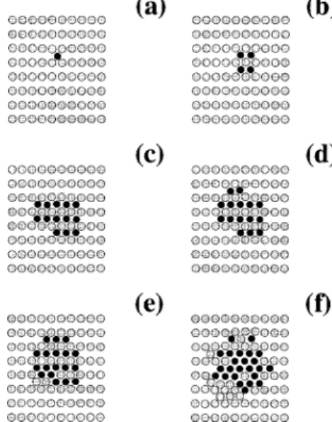
The sharp tip is pushed when its separation from the Cu~110! surface is 4 Å. In Fig. 2 we show the variation of the normal force FN~along the z direction! with the push ~or
downwards displacement of the tip, d5pdDz, pd being the number of increments!. The sign of the attractive force is taken negative. The atomic structure of the junction are il-lustrated in Fig. 3 for relevant stages of the contact and in-dentation. At large separation, FN;0 owing to the short-range nature of interaction forces; but it becomes attractive and increases with increasing d, passes through a minimum and then decreases. The interaction of the single Ni atom at the apex, that faces the substrate, dominates the force varia-tion. In agreement with the ab initio calculations21 FN
de-creases because the apex of the Ni tip enters the repulsive range. The electronic contact, where the electronic structure and hence electronic charge density are modified owing to the interaction between outermost Ni and Cu atoms, sets in for d.1.3 Å. For d*3 Å, the effective potential barrier Feff
collapses to allow the ballistic conductance. The first fall of FN denoted by J1 corresponds to the jump of the apex Ni
from its metastable position to the hollow (H) site. This situation indicates that a mechanical contact is established between the tip and the sample surface. At d54.3 Å four Ni atoms~apex atom and three atoms in the second layer of the bare asperity! move to the H sites of the substrate and be-come in registry with the Cu~110! planes. The Ni atoms in the layer following the contact occupy bridge sites and keep their hexagonal structure, but their registry with the adjacent Ni layers of the asperity is destroyed. The attractive force decreases quasilinearly with the increasing push in the region 4.3 Å,d,5.7 Å. At d;5.8 Å the atomic structure and the layers near the contact becomes disordered and eventually one layer of the Ni asperity disappears. This is a yield that causes to the sudden fall of FN labeled by J2.
FIG. 1. Schematic description of the Ni~111! tip ~or asperity! and the Cu~110! substrate. The dark and light gray balls represent the Ni and Cu atoms, respectively. The Ni~111! and Cu~110! atomic planes are parallel to the xy plane. The long side of the ~110! rectangle is parallel to the x axis.
FIG. 2. Variation of the normal force FN versus the downward
displacement ~or push! d. J1,J2, . . . indicate the features
associ-ated with sudden change in FN. The attractive and repulsive range
Between J2 and J3, FNdecreases again with d~or push!, and
displays also a quasilinear variation; the Cu atoms at the contact are gradually displaced from their original positions, and the atoms in the first layer lose their registry. This situ-ation lasts until d57.2 Å, where the area of the contact in-creases and the first Ni layer becomes in registry with the substrate. At the end, the attractive FN increases suddenly.
Further variation of FN is not regular ~for d.7.2 Å!, and
attractive FNgenerally decreases with increasing d ~or pd) if
the number of layers does not change. On the other hand, the attractive FN increases if the two adjacent layers of the
as-perity merges into one layer, or the number of asas-perity atoms at the contact increases or disordered atomic structure be-comes ordered. It is seen that for 0,d,10 Å, FN(d) is
generally in the attractive range; displays multiple ~or se-quential! jump-to-contact phenomena in the attractive range. Tip atoms having relatively lower coordination can lower the total energy by moving to the substrate surface and forming a commensurate layer. The growth of the contact is easier for a sharp tip as in the present case. Moreover, while the repul-sive forces act on the contact layer, the atoms in the layer above the contact become in the attractive range. Initially, the contact area A is relatively smaller; the resulting force becomes attractive. Beyond certain value of A ~i.e., contact involving 23 Ni and Cu atoms and thus d.10 Å! FN(d)
varies but always stays in the repulsive range. The elastic stiffness constants of the bulk Ni along @111# direction and that of the bulk Cu along @100# direction are (C1112C12
14C44)/353.6nN/Å2 and C1151.7nN/Å2, respectively.
Both values are relatively larger than that of the junction
estimated from Fig. 2. This implies that the discrete nature of the junction and its atomic structure becomes crucial for the small contacts.
The atom exchange,19in which substrate atoms~Cu! raise to the contact interface ~i.e., first layer above the substrate surface! and to the layers above it while the Ni atoms of the asperity dip into the substrate, starts to occur at the beginning of the repulsive range and increases with the deformation of the substrate. This process contribute to the growth of A. The contact area grows discontinuously; in different stages of the contact and subsequent indentation the contact interface in-corporates 1,4,8,13,15,18,23, . . . atoms. Interestingly, the growth of the contact in terms of new atoms brought into the interface, i.e., Ai112Ai, does not present a regular pattern
and involves more then one atom. The dissapearance of an asperity layer gives rise to a sudden change of the force, i.e., sudden increase~decrease! in the attractive ~repulsive! range. However, not all the sudden changes of FN(d) are associated
with the dissapearance of a layer. The evolution of the con-tact is illustrated by Fig. 4, where we note that the significant deformation of the interface starts to occur in the repulsive force range.
The simulation of indentation25 in the Au~001! @also Ni~001!# sample produced by the blunt Ni~001! @also Au~001!# tip at T5300° K revealed that the deformation occurs in the softer metal. In the present study the sequential
~multiple! jump-to-contact phenomena and the deformation
induced therefrom occur in the sharp tip even it is harder than the sample. As seen in Fig. 2, the multiple jump-to-contact phenomena yield an average attractive force in a rather long-range displacement of the sharp tip even though the deformed apex of the tip is under the action of the repul-sive force. The puzzling results29 of the measurements of force between the Si~111! tip and the Si~111! sample can be explained by the deformation of the sharp tip yielding the FIG. 3. Side views of the atomic structure for the Ni~111! tip ~or
asperity! and the Cu~110! substrate are illustrated for various stages of the indentation. The tip is pushed from a distant separation to-wards the sample surface in increments of Dz. The downwards displacement of the tip is d5pdDz. ~a!, ~b!, ~c!, ~d!, ~e!, ~f!, ~g!, and
~h! correspond to d57.1, 7.2, 8.0, 8.7, 11.1, 11.5, 12.2, and 12.9 Å, respectively. The Ni and Cu atoms are shown by filled and empty circles, respectively.
FIG. 4. Top views of the atomic structure at the interface of the contact are shown for various stages of contact and indentation. Substrate atoms in the surface and tip atoms in the contact interface are shown by large gray and small dark circles, respectively. The panels ~a!, ~b!, ~c!, ~e!, and ~f! correspond to d50.9, 5.2, 8.7, 9.2, 9.9, and 11.5 Å, respectively. The atom exchange are seen in the panels in~e! and ~f!.
force variation similar to that in Fig. 2. In order to examine the variation of two-terminal conductance through a point contact created by Ir~111! tip, Todorov and Sutton7 carried out atomic scale simulations of the indentation and found that the contact grows discontinuously. Present work pro-vides a detailed analysis for the growth of the contact and its atomic structure.
B. Pulling off
At certain stage of the indentation we stop lowering the tip, and start to move it away from the substrate in the posi-tive z direction. This way the junction formed by indentation is stretched and a connective neck is formed.17,25,30This neck becomes narrower with the stretch~or pull u5puDz, pu
be-ing the number of increments! and eventually is broken. We investigated the pulling off the junction from two different stages of the indentation, described in Sec. II A, i.e., d
510.1 Å and d513.6 Å. In the latter, A is relatively larger
and the deformation at the junction is more pronounced. We first consider the former case, i.e., small size indentation made by a sharp tip. In Fig. 5 we show the variation of the tensile force FN(u) with the stretching. Figures 6 and 7 show side and top views of the atomic structure at the relevant stages of the stretch and reveal new and interesting features. In agreement with the earlier studies5–7,31 FN(u) curve
shows abrupt changes. However, in contrast to the earlier studies each of these changes are not associated with the creation of a new layer. Furthermore, these changes do not exhibit a regular pattern with u. On the other hand, the completion of a new layer give rise to an abrupt decrease in FN(u). Before the formation of a new layer the structure of
the neck becomes disordered, and eventually a new layer is formed. This is the yielding of the neck. As pointed out by earlier studies,7,25,31,32 the yielding and subsequent creation of a new layer is mediated by the disorder-order transforma-tions in the nanowires with cross section incorporating only a few atoms as in the present case. Between two consecutive yielding of the neck FN(u) increases linearly. That is
attrib-uted to the quasielastic straining of the neck. In the present case, where T54 K and the initial junction is narrow ~or A is small!, disorder-order transformations are usually sudden, but require significant stretching; in the meantime, different intermediate situations~such as transformation of an incom-plete layer or generation of interstitial atoms, etc.! occur. At
the beginning of the pulling of the junction, five dynamic layers of mainly Ni with some mixture of Cu atoms can be identified. For small u, FN(u) varies linearly; ]FN/]u is
large and hence requires a strong force to induce the first structural change U1. However, U1displays an intermediate situation, and only after U2 an additional layer is identified.
Between U1 and U2, ]FN/]u is reduced, and continues to
reduce in the following quasielastic stages. The next new layer forms at U3 and stays stable until U4, but transition
from seven-layer to eight-layer structure is completed be-tween U4and U5. After U5, the junction has eight Ni layers
above the substrate. Interestingly, the neck is formed from two pentagons ~layers 4 and 5! and a quadrangle ~sixth layer!. Single atoms located between these layers form a string passing through the centers of pentagons and quad-rangle. This low-temperature intermediate structure FIG. 5. Variation of the tensile force FN versus the upwards
displacement or pull u (u5puDz) in a connective neck formed by
the pulling-off the sharp tip from an indentation. U1, U2, . . . U6
are relevant features that are explained in the text.
FIG. 6. Side-view snapshots of the atomic structure for the rel-evant steps of pulling the Ni tip from an indentation. The pulling-off starts from an indentation corresponding to d510.1 Å. The panels~a!, ~b!, ~c!, ~d!, ~e!, ~f!, and ~g! correspond to u5 0.7, 2.1, 4.2, 5.6, 6.3, 7.7, and 10.5 Å, respectively.
FIG. 7. Top and side views of the atomic structure during the formation of the connective neck.~a! Atomic structure of the sub-strate surface and the contact interface. Circles with the sharp and dotted circumferences are Ni and Cu atoms, respectively. In the gray scale, the higher the atoms are, the lighter become their color. ~b! The top view of atoms at the neck forming pentagon, quadrangle and single atoms between them.~c! Side view of the neck.
earlier ab initio calculations for single atom contact. In the course of stretch of the neck the structure of the interface
~that is in contact with the substrate surface! does not change
significantly and stays in registry with the Cu~110! structure. Moreover, the layers of the Ni pyramid that stayed on the substrate after the break, becomes also pseudomorphically commensurate with the Cu~110! structure. As for the Ni as-perity that remains after the break of the neck, a few layers keep their hexagonal structure commensurate with the Ni~111! plane, except the pentagonal structure maintained at the bottom of the asperity.
Pulling from a higher level of indentation (d513.6 Å in Sec. II A! starts from a junction that has relatively larger A and more pronounced deformation, and displays similar fea-tures with following differences. In the latter the tensile force at the initial stage of stretch reach to higher level (FN;14 nN! owing to relatively larger contact area, but the amount of stretching achieved until the break is relatively smaller. In contrast to the previous pulling off from the low level of indentation ~i.e., d510.1 Å!, the Ni pyramid stayed on the substrate is relatively large while the Ni asperity becomes relatively smaller.
C. Sliding friction
To investigate the friction and wear of a single metal as-perity on an incommensurate metal surface we used the same system that was considered in Secs. II A and II B. The as-perity is first pushed to the Cu~110! surface along the z di-rection and then is slit along the x didi-rection under the con-stant loading force FN52.64 nN distributed on the top plane of the asperity. The displacement of the asperity after ps
increments is s5psDx. The temperature is kept fixed at 4 K. Upon the formation of steady state contact between the Ni asperity and the Cu surface the energy of the whole system is lowered by;22 eV. The energy lowering originates mainly from the adhesive interaction. The atomic rearrangements during the development of the junction between the Ni as-perity and substrate prior to sliding follows the similar events described in Sec. II A. The aspects that are relevant for the sliding are briefly summarized. Once the contact is estab-lished, the layer structure of the pyramid remains, but single atom at the apex and the subsequent layer disappears leaving only eight Ni layers including the contact layer~interface! at the surface of the substrate ~as described in Fig. 1!. While some Ni atoms substitute Cu atoms at the contact, some of them are accumulated behind the asperity. On the other hand, some Cu atoms migrate into the Ni asperity. The Cu~110! surface at the contact region can be viewed as a Cu-Ni alloy with the lattice structure of the Cu~110! surface. In spite of the fact that the cohesive energy of Ni ;30% higher than
that of Cu crystal, two layers of the Ni pyramid which are adjacent to the Cu~110! surface have changed from the Ni~111! lattice structure and become matched the Cu~110! substrate. The distance between these layers comply with that of the Cu~110! planes. This is perhaps due to the lower coordination numbers of the Ni atoms near the apex. The remaining top five layers of Ni asperity keep their original Ni~111! lattice structure.
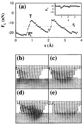
The sliding starts after the atomic configuration of the contact reached the steady-state condition; the asperity is translated by the increments ofDx. The variation of the lat-eral force FLwith the displacement s is shown in Fig. 8. By
definition, the sign of FL(s) resisting to the sliding is taken
negative. We note the following interesting features:~i! The abrupt changes of the FL(s) curve display a quasiperiodic
variation with a period of approximately 3.5 Å. Two features of different characters ~labeled T and M) occur consecu-tively in each period; these are noticed by the fact that FL(s)
decreases and changes sign with the displacement of the as-perity.~ii! Between two consecutive features ~from Tnto Mn
or from Mn to Tn11) FL(s) first decreases ~where FL.0)
and then increases ~where FL,0) with displacement s; it displays a quasielastic behavior.~iii! The work done against FL(s) over a period from Tn to Tn11, i.e.,2*Tn
Tn11
FL(s)ds,
increases from period to period. This deviation from the Amonton’s law is explained by the growth of the junction. The variation of lateral force showing the elastic ~or linear! region followed by an abrupt decrease is a peculiarity of the stick-slip process in dry sliding friction that occurred in cer-tain ideal conditions so far. It is of particular interest since the sliding of a metal asperity on an incommensurate metal surface is shown to give rise to a stick-slip behavior. Since the asperity forms a finite-size contact with ordered structure, the occurance of a quasiperiodic stick-slip behavior cannot be explained by the sharpness of the asperity. It is rather due to the fact that the cubic lattice parameters of Ni and Cu vary within;2.5% (aNi53.52 Å and aCu53.61 Å!. Moreover all
edges of the~111! unit cell has the same length as the shorter edge of the ~110! unit cell (a/
A
2). Under these circum-stances, the sliding of a Ni asperity follows a special path on the Born-Oppenheimer surface that passes through certain structural phases explained below. However, we expect that the stick-slip behavior in Fig. 8 can be washed out if the FIG. 8. Variation of the lateral force with the sliding s of the Ni~111! asperity on the Cu~110! surface. The average lateral force F¯
L~or friction force! is shown by dashed line. Tnand Mnindicates
different type structural transformation in the nth period. FL(s)
sliding involves multiple asperity. Very large contacts ~that is unusual for an asperity! can give rise to misfit dislocation. Snapshots of side views and x y projections of the atoms in the layers where the sliding takes place are shown in Fig. 9, only for T1 and M1 features. Figure 9~a! depicts atomic
configuration essentially before T1, but after the onset of
contact. As a result of sliding, the top four planes are dis-placed along the x direction and also slightly lowered. This changed the registry between the fourth and fifth Ni~111! layers from the top; the energy of the system is raised and perhaps exceeded that of another structure. Eventually, as shown in Fig. 9~b!, the fifth layer from the top, which was initially commensurate with the Ni~111! layers, undergoes a structural transformation and becomes matched the lower Ni layer that was already changed to the lattice structure of the Cu~110! plane. The xy projection of atoms in this particular layer that changed its lattice structure through T1is shown in
Fig. 9~e! before and after the transformation. One row of Ni atoms moved sideways, the next went ahead and third one merged to the lower layers. During this
incommensurate-commensurate structural transformation, while part of the stored energy is kept in the new phase, the rest of it is re-leased in the nonadiabatic transition and dissipated perhaps by exciting nonequilibrium phonons. The amount of energy dissipated in this transition is calculated ;3 eV. The force FL(s), which was initially resisting the sliding, is lowered
suddenly during the transition and changed its direction. The above variation of FL(s) is reminiscent of the stick-slip
mo-tion, but the rearrangement of the atoms leading to an or-dered structural transition is rather unexpected. After the transition T1,uFL(s)u increases quasi-linearly with the
dis-placement of the asperity. Once the asperity moves approxi-mately 2 Å, or by the height of the 2D hexagonal unit cell of the Ni~111! planes, the stick behavior ends and the slip starts with the second structural transition M1. The side views of
the atoms before and after the transition M1 are shown in
Figs. 9~c! and 9~d!; those corresponding to xy projections are presented in Figs. 9~f! and 9~g!. Two asperity layers both were commensurate with the Cu~110! plane @i.e., one pro-duced by the transition T1 as explained above and the
Ni~110! layer below it# merge into a single ~111! layer of Ni. The transition starts in front of the Ni asperity and ends at its back, and uFL(s)u decreases abruptly. Note that upon this latter structural transition, one layer of asperity disappears and hence the slip ends with a wear. During the stick stage from T1 until the onset of M1 the energy of motion is con-verted into the potential energy and is stored as the strain energy ofDEs;2.8 eV. While part of DEsis kept in the new phase on the Born-Oppenheimer surface as a result of the structural transition labeled by M1, the major part,DEd;2
eV, is, however, released to generate local nonequilibrium phonons and hence is dissipated in the whole system. After M1, FL(s) increases again linearly with s; same events
re-peat leading to transitions T2 and M2. At each period, the
asperity loses one layer, so its contact area with the Cu~110! surface further increases.
The incommensurate-commensurate structural transition illustrated in Fig. 9 have interesting features. The transition occurs in a short time interval; starting from one ordered 2D structure it ends up in a different ordered atomic structure. In the course of these transitions, the energy of the system makes a sudden change. These features suggest that each structural transition is associated with a first-order phase transition and corresponds to local minimum in the Born-Oppenheimer surface. This conclusion is strengthened by the analysis of the structure factor,33 S(qW).
In closing this part we comment on the following points:
~i! The junction between the asperity and the Cu surface is
growing with sliding. The cross section of the contact A is in the range of ;plF2, where the electronic states are quan-tized in the x y plane with a level spacing ;103 K. The number of contact states that dip below the Fermi level, EF
depends strongly on A and its shape, and the conduction channels derived therefrom are intermixed owing to the tun-neling and scattering.22,34 Therefore, the ballistic conduc-tance of the contact, G(s) cannot yield sharp quantized step structure even if the contact would evolve adiabatically with sliding. However, G(s) is expected to show abrupt jumps only due to the discontinuous growth of the junction through the T- and M -type phase transitions in the course of sliding. FIG. 9. Side view of atomic structure calculated for the Ni~111!
asperity ~dark gray circles! sliding on the Cu~110! surface ~light gray circles!. Panels ~a! and ~b! are before and after the structural transformation T1; Panel~c! and ~d! are before and after the
struc-tural transformation M1. Only part of the substrate is shown. Panel
~e! shows the xy projection of the atoms in the Ni layer experienc-ing a structural transformation. Light gray circles correspond to the fifth Ni~111! layer from the top before T1; after T1 this layer is
changed to the Ni~110! that is commensurate to the Cu~110! as shown by the dark circles with dotted circumference. Panel ~f! shows the two Ni~110! layers corresponding to the situation in ~c! before the transformation M1. These two layers merged into one
Ni~111! layer in panel ~g! as described by the side view ~d! after M1.
By measuring FL(s) and G(s) simultaneously in the course
of sliding one can provide additional information about the contact. ~ii! As the sliding continues, a cluster of atoms grows at the contact behind the asperity. The atoms of this cluster are not usually in disordered state. ~iii! The sliding occurs at the interface between Ni~111! plane and Ni~110! plane matched to the Cu~110! plane, since the relative mo-tion between the ~111! planes requires relatively lesser en-ergy. ~iv! The average friction force F¯L is calculated for 0,s,11 Å to be 22.06 nN. ~v! Finally, we note that the usual stick-slip behavior was also obtained in the earlier simulation of the Si~111! tip sliding on the Si~111! surface.35 Here, the sliding leads to wear and two stick-slip stage in each period are associated with different structural transfor-mations. The mechanism of wear and accumulation of mate-rial behind the tip are also results revealed from the present study.
III. BLUNT TIP
The blunt tip is constructed from a hemisphere compris-ing 1580 Ni atoms, which are arranged initially in 14 Ni~001! planes. The dynamic atoms are in the first nine lay-ers from the bottom; the remaining five Ni~001! layers at the top are robust. The bottom of the hemisphere is flat and the lowest Ni~001! layer includes 24 Ni atoms facing the surface of the substrate. The substrate by itself is made from 10 Cu~001! planes; each plane including 200 Cu atoms, alto-gether 2000 Cu atoms. The last~bottom! three Cu~001! lay-ers are robust. The Ni~001! planes as well as the Cu~001! planes are parallel to the xy plane. The present case is dif-ferent from that of the sharp tip, since the Ni~001! planes are pseudomorphic to the Cu~001! planes. The lowest part of the tip being flat, the Ni and Cu atoms have similar coordination numbers and the hemisphere exerts strong forces on the sub-strate and can sustain strong forces without significant defor-mation.
A. Contact and indentation
The Ni hemisphere~with flat bottom! is lowered by incre-ments ofDz50.1 Å; between two consecutive increments all the dynamic atoms ~in the Ni hemisphere and in the sub-strate! are relaxed for 500 time steps. When the separation between the lowest layer of the Ni hemisphere and the Cu surface is in the range of the cubic lattice parameters a (.3.5 Å!, a significant attractive ~adhesion! force is gener-ated; that causes, in particular, the Cu atoms facing the Ni
hemisphere to jump to contact. It can be understood by the fact that the elastic stiffness constant C11 of the Cu and Ni crystals are 1.8 and 2.6 nN/Å2. The jump to contact is clearly seen in Fig. 10~a!, in which FN attained ;25 nN within a small displacement d. Subsequent to the jump to contact FN
decreases in the attractive range with increasing d. Multiple jump to contacts of the sharp tip in Fig. 2 do not occur in the present situation. While the Ni atoms forming the contact with the substrate enters gradually to the repulsive range, the Ni atoms slightly above the contact are still in the attractive range. In the repulsive range, the substrate atoms under the contact is lowered while surface atoms around the contact raised under the attractive interaction with the Ni atoms. The massive deformation at the close proximity of the contact occurs in the repulsive range, and it involves the substrate atoms under the contact area as seen in Fig. 10~b!. In the hemisphere, all the Ni atoms except those near the center are displaced. The plastic deformations are induced by disloca-tions in the hemisphere and by slips both in the hemisphere and in the substrate. Fig. 10~c! illustrates the formation of slip planes. We note that FN(d) is piecewise linear in the
interval 2,d,7 Å. The yielding occurs for d;7 Å; the Ni layers are deformed as a result of compressive strain, and eventually become disordered. Subsequently, the layer struc-ture is recovered, but one layer of the hemisphere disappears and the contact area increases. In the meantime, the Cu and Ni atoms start to mix in the interface.
B. Sliding
The sliding of the blunt Ni tip described in Sec. III on the Cu~001! surface is investigated under the loading force FN
59.1 nN and FN512.9 nN. The lowest atomic plane of the
blunt tip, which includes 24 Ni atoms, is initially in contact with the Cu~001! surface. The interface created by these at-oms are rather large and flat. Therefore, the sliding friction is expected to be different from the friction of a sharp tip, treated in Sec. II C.
These two surfaces, i.e., the Ni~001! and Cu~001!, are pseudomorphic, but their elastic parameters and binding en-ergies are different. In this respect, the relative motion of these two surfaces and resulting friction may involve inter-esting features. Here the diagonal of the primitive square unit cell is taken parallel to the x direction. In Fig. 11~a! we show the variation of the lateral force under the constant normal loading force, FN59.1 nN. The variation of the normal re-action force that is calculated in the course of simulations is presented by the inset. It demonstrates that the operation un-FIG. 10. ~a! Variation of the perpendicular force with the displacement of the Ni hemisphere making a contact and then indentation on the Cu surface.~b! Side views of the atoms during indentation under the repulsive perpendicular force FN524 nN. ~c! Side view of atoms
der the constant loading force mode is well simulated. Figs. 11~b!–~e! show the atomic structure before and after the slip for different loading forces. We note that in Fig. 11~a! the ratio of the static friction force FLS and average kinetic fric-tion force, F¯f, i.e., FL
S/ F¯
f;2. In the low loading ~i.e., FN 59.1 nN! case the Ni surface is initially stuck on the Cu
surface; whole Ni hemisphere and the Cu surface are sheared and line dislocations are generated on the substrate surface below the contact interface until the slip sets in. During slip the atomic structure at the contact becomes disordered, some Cu and Ni atoms are exchanged and the hemisphere is dis-placed along the @110# direction. Eventually the regular structure at the contact is recovered upon the jump of the Ni atoms at the interface to their new positions. These events take place in a short interval, and the lateral force FL
de-creases by ;15 nN. As the sliding continues following the slip the hemisphere and the substrate at the junction are sheared again in the new stick stage started at T. While in the front of the hemisphere the junction becomes disordered and more atoms are exchanged, in the back the slips occur on the Ni~111! planes. At the end, the quasilinear increase of the lateral force FL(s) stops with the start of the slip stage; it decreases suddenly while the Ni atoms at the contact jump to the next position by moving along the @11¯0# direction. For large FN, the generation of dislocation and slip planes in the
hemisphere become pronounced in the sliding motion; this way the stick-slip motion becomes less regular.
IV. CONCLUSIONS
We presented the detailed analysis of contact formation, indentation, subsequent pulling and dry sliding friction of the Ni tip on the relatively soft Cu surface. We investigated the effect of tip geometry ~sharp or blunt!, crystal structure of the tip and sample, and discovered the following important features:~i! Upon the onset of the contact of a sharp tip the multiple jump to contact events can occur in the attractive regime of the normal force. The Ni layers~or atoms! near the apex engage in the jump to contact phenomena even though the elastic stiffness constants of Ni are larger than those of Cu. Already with the onset of the contact, atoms from the lower planes of the asperity become matched to the substrate lattice structure. The situation is reversed if the tip is blunt with large area of contact. In this case, mainly the Cu atoms on the surface jump to contact in a single event. ~ii! Inden-tation proceeds in the repulsive force range. For a sharp tip the perpendicular force displays quasilinear variations fol-lowed by a sudden decrease caused by disappearance of a layer, or other structural changes. The junction grows dis-continuously and, in general, suddenly by the implementa-tion of the new atoms to the interface. However, the number of atoms that are brought to contact is different for each growth event. It is interesting to explore whether the growth of the contact in terms of these new atoms is correlated with the electronic contact states dipping into the Fermi level. Such effects were explored earlier by 2D metals.1 In the indentation of the flat tip the sudden force variations ~or yields! are not so frequent and occurs mainly through the slips on the atomic planes.~iii! The atom exchange, in which the substrate and the asperity atoms change their positions occurs in the repulsive force range and increases with in-creasing deformation. ~iv! Pulling off from an indentation occurs in the attractive ~tensile! range of the perpendicular force. The connective neck first forms through interesting atomic rearrangements and then is broken leaving a Ni py-ramidal asperity on the Cu surface, that is lattice matched to the substrate. ~v! During the pulling off, the tensile force exhibits abrupt changes. However, each of these changes are not associated with the creation of a new layer. Sometimes, a single atom implemented between two adjacent layers in-duces additional structures in force variation. ~vi! In the dry sliding of a sharp Ni~111! tip ~or asperity! on the Cu surface under constant loading force the lateral force exhibits quasi periodic variation; each period consists of two different stick-slip process involving structural phase transitions. While one layer of asperity changes and matches the sub-strate lattice in the first slip, two asperity layers merge into a one through structural transition during the second slip. This leads to wear. While the relative motion occurs between the regular plane and the substrate matched plane of the asperity, the strain energy is stored at the interface.~vii! The sliding of a flat Ni~001! surface on the Cu~001! surface depends on the loading force. In the low loading case, the lateral force dis-plays quasilinear variation in the stick stage that is followed by the sudden decrease in the slip stage. For large loading, the stick-slip motion is less regular.36
FIG. 11. ~a! Lateral force FL vs the lateral displacement s
cal-culated for the Ni hemisphere sliding on the Cu~001! surface under the loading force, FN59.1 nN. The inset show that the loading
force does not vary significantly. FLis the lateral force before the
first slip stage begins. T indicates the point where the first slip ends and the second stick stage starts.~b! and ~c! show the side view of atomic structure in the stick stages before and after a slip taking place under the loading force, FN59.1 nN. Ni and Cu atoms are
shown by filled and empty circles.~d! and ~f! are stick stages before and after a slip taking place under a larger loading force, FN
S. Ciraci and E. Tekman, Phys. Rev. B 40, 11 969~1989!.
7T. N. Todorov and A. P. Sutton, Phys. Rev. Lett. 70, 2138~1993!;
A. M. Bratkovsky, A. P. Sutton and T. N. Todorov, Phys. Rev. B 52, 5036~1995!.
8K. L. Johnson, Contact Mechanics~Cambridge University Press,
Cambridge, 1986!.
9S. Ciraci, in Tip-Surface Interactions in Scanning Tunneling
Mi-croscopy and Related Methods, Vol. 183 of NATO Advanced Study Institute, Series E: Applied Science, edited by R. J. Behm, N. Garcia, and H. Rohrer~Kluwer Academic, Dordrecht, 1990! p. 113; E. Tekman and S. Ciraci, Phys. Rev. B 40, 10 286 ~1989!; E. Tekman and S. Ciraci, Phys. Scr. 38, 486 ~1988!.
10C. M. Mate, G. M. McClelland, R. Erlandsson, and S. Chiang,
Phys. Rev. Lett. 59, 1942~1987!.
11For a current review see, for example, Physics of Sliding Friction,
Vol. 311 of NATO Advanced Study Institute, Series E: Applied Science, edited by B. N. J. Persson and E. Tosatti~Kluwer Aca-demic, Dordrecht, 1996; Micro/Nanotribology and its Applica-tions, edited by B. Bhushan ~Kluwer Academic, Dordrecht, 1997!.
12G. J. Germann, S. R. Cohen, G. Neubauer, G. M. McClelland,
and H. Seki, J. Appl. Phys. 73, 1~1993!; S. Fujisawa, E. Kishi, Y. Sugawara, and S. Morita, Phys. Rev. B 51, 7849~1995!.
13M. Hirano and K. Shinjo, Phys. Rev. B 41, 11 837~1990!. 14M. Hirano, K. Shinjo, R. Kaneko, and Y. Murata, Phys. Rev. Lett.
67, 2642~1991!.
15
K. Shinjo and M. Hirano, Surf. Sci. 283, 473~1993!.
16S. R. Cohen, G. Neubauer, and G. M. McClelland, J. Vac. Sci.
Technol. A 8, 3449~1990!.
~1990!.
22E. Tekman and S. Ciraci, Phys. Rev. B 43, 7145~1991!. 23E. Tekman and S. Ciraci, Phys. Rev. B 42, 1860~1990!. 24F. F. Abraham, I. P. Batra, and S. Ciraci, Phys. Rev. Lett. 60,
1314~1988!.
25U. Landman, W. D. Luedke, N. A. Burnham, and R. J. Colton,
Science 248, 454~1990!.
26M. Brandbyge, J. Schio
”tz, M. R. So”rensen, P. Stoltze, K. W. Jacobsen, and J. K. No”rskov, Phys. Rev. B 52, 8499 ~1995!.
27For a critical review see also A. P. Sutton, Curr. Opin. Solid State
Mater. Sci. 1, 827~1996!.
28M. S. Daw and M. I. Baskes, Phys. Rev. B 29, 6443~1984!; S. M.
Foiles, M. I. Baskes, and M. S. Daw, ibid. 33, 7983~1986!; M. S. Daw, ibid. 39, 7441 ~1989!. We used the embedded atom model potentials for Cu and Ni developed in the above works.
29S. P. Jarvis, H. Yamada, S. I. Yamamoto, H. Tokumoto, and J. B.
Pethica, Nature~London! 384, 247 ~1996!.
30J. K. Gimzewski, R. Mo¨ller, D. W. Pohl, and R. R. Schlitter, Surf.
Sci. 189, 15~1987!.
31H. Mehrez, M.S. thesis, Bilkent University, 1996.
32H. Mehrez and S. Ciraci, Phys. Rev. B 56, 12 632~1977!; J. Phys.
9, 10 843~1977!.
33A. Buldum and S. Ciraci, Phys. Rev. B 55, 12 892~1977!. 34H. Mehrez, S. Ciraci, A. Buldum, and I. P. Batra, Phys. Rev. B
55, R1981~1997!.
35
U. Landman, W. D. Luedke, and A. Nitzan, Surf. Sci. 210, L177 ~1989!.