i.. í^;¡:· ;ï'îî у·'·, ” -■■■·:■ к-it ' . ί ; 4U '(іш‘ " . r ‘ 1 " 4 : ''.r Л 1 i 1 І ! { У" « :;■ ' H ; :*· '>··ν "! i t o M.. j vt k,; , ¿ ''w .w L * » « , / > ■ (’. •.li.if? '·: “ ';■' Г · '; 1 ir : ·· ·' ·» .'· * 4*ί^ · «· : (TV ' ··*·· q / / 9 s < l
•A78
У
5
?
tâB8
NOISE ANALYSIS OF INTERDIGITAL CANTILEVERS FOR
ATOMIC FORCE MICROSCOPY
A DISSERTATION
SUBMITTED TO THE DEPARTMENT OF ELECTRICAL AND ELECTRONICS ENGINEERING
AND THE INSTITUTE OF ENGINEERING AND SCIENCES OF BILKENT UNIVERSITY
IN PARTIAL FULFILLMENT OF THE REQUIREMENTS FOR THE DEGREE OF
DOCTOR OF PHILOSOPHY
By
G. Gokseniii Yaraliogiu
October 6, 1998
I certify that I have read this thesis and that in my opinion it is fully adequate, in scope and in quality, as a thesis for the degree of Doctor of Philosophy.
Alxlullah Atalar, Ph. D. (Supervisor)
I certify that I have read this thesis and that in my opinion it is fully adequate, in scope and in quality, as a thesis for the degree of Doctor of Philosophy.
Hayrettin Koymen, Ph. D.
I certify that I have read this thesis and that in m.y opinion it is fully adequate, in scope and in quality, as a thesis for the degree of Doctor of Philosophy.
Orhan Aytiir, Ph. D.
I certify that 1 have read this thesis and thcit in iiiy opinion it is fully adequate, in scope and in quality, as a thesis for the degree of Doctor of Philosophy.
Ekmel Ozbay,
I certify thcit I have read this thesis and that in my opinion it is fully adequate, in scope and in quality, as a thesis for the degree of Doctor of Philosophy.
Gozde Bozdagi, Ph. D.
Approved for the Institute of Engineering and Sciences:
Prof. Dr. Mehmgj/^aray
Director of Institute of Engineering and Sciences
ABSTRACT
NOISE ANALYSIS OF INTERDIGITAL CANTILEVERS FOR
ATOMIC FORCE MICROSCOPY
G. Göksenin Yaralioglii
Ph. D. ill Electrical and Electronics Engineering
Supervisor: Prof. Abdullah Atalar
October 6, 1998
Atomic force microscoiDe (AFM) is proved to be a powerful tool for atomic resolution surface imaging. The most crucial parts of an AFM system are the cantilever with an integrated tip and the deflection detection sensor. AFM systems measure deflections that are comparable to atomic dimensions using technicpies such as tunneling, interferometry, piezoresistive sensing and optical lever detection. Interdigital (ID) cantilevers are the most recently introduced method which makes use of its interferometric nature to improve deflection detection sensitivity. Basicallj^ ID cantilever is composed of two sets of interleaving fingers which create an optical phase grating. In this thesis, a detailed analysis of ID cantilevers will be presented. The theory underlying the o[)eration of the phase gratings with the response curves curd confirming e.xperimental results will be formulated. The noise performance of the ID cantilever will be compared to the optical lever detection method. We will present a new method for the mechaniccd noise calculation by using the analogy between electrical circuits and mechanical structures. This new method will be applied to the AFM cantilevers to calculate the noise correlation on the cantilever surface. We will also present the signal to noise ratio (SNR) calculation method on the cantilever. One of the basic problem of the all AF'M systems is the speed limitation due to single AF'M tip scanning at relatively low frequencies yielding low throughput. A direct approach to this problem is the operation of cantilever arrays instead of one cantilever. In this thesis, we will also present the electronics for cantilever arrays which increases the throughput of the AFM systems.
Keyioords: Atomic Force Microscopy, Interdigital cantilever. Deflection Detection.
Optical Phase Grating, Mechanical Noise Analysis, Cantilever .'\rrays.
ÖZET
a t o m ik k u v v e t m ik r o s k o b u iç in b ir b ir in e g e ç m iş
PARMAKLI KALDIRAÇLARIN GÜRÜLTÜ ÇÖZÜMLEMESİ
G. Göksellin Yaralıoğlu
Elektrik ve Elektronik Mühendisliği Doktora
Tez Yöneticisi: Prof. Dr. Abdullah Atalar
6 Ekim 1998
Atomik ktıvvet mikroskobunun (AKM), atomik çözünürlükte yüzey resimlenmesi için güçlü bir alet olduğu kanıtlanmıştır. Bir. AKM sistemiııin en önemli kısımları bir iğne birleştirilmiş kaldıraç ve bükülme ölçen algılayıcıdır. AKM sistemleri tüııelleme, girişim, piezodirenç algılama, ışık kaldıracı gibi yöntemleri kullanarak atomik ölçekte bükülmeleri ölçebilirler. Girişimi kullanan birbirine geçmiş parmaklı (BGP) kaldıraçlar en son önerilen yöntemdir. Temel olarak, BGP kaldıraç oııtik faz mazgalı oluşturmak için birbirine geçmiş iki takım pa.rma,ktan oluşur. Bu tezde, BGP kaldıra.çların detaylı bir çözümlemesi sunulacak ve optik faz ınazgallarmm çalışına ilkesi yanıt eğrileri ve deneysel sonuçlarla beraber formüle edilecektir. BGP kaldıracının gürültü başarımı da ışık kaldıracı yöntemi ile karşılaştırılacaktır. Aynı zamanda, mekaııiksel gürültü hesaplan ması için, mekanik sistemlerle elektrik devrelerindeki benzerliklere da.yana,ıı yeni bir yöntem de gösterilecektir. Bu yöntem kullanılarak AKM kaldıraçlarının yüzeyinde gürültü ilintisi ve işaret gürültü oranı (IGO) hesaplanacaktır. AKM sistemlerindeki en önemli sorunlardan birisi de tek bir AKM kaldıracının düşük sahınmlarda tarama yapmasından kaynaklanan hız limitidir. Bu problem kaldıraçların paralel çalışması ile çözülebilir. Ayrıca bu tezde, kaldıraç dizilimleri için elektronik devreler de sunulacaktır.
Anahtar Kdirneler: Atomik Kuvvet Mikroskobu, Birbirine Geçmiş Pcirma.k]ı Kaldıraç,
A C K N O W L E D G M E N T S
Man}^ people contribute to the development of this thesis. But above all, I would like to especially thank to my supervisor Professor Abdullah Atalar for always generating new ideas, encouraging me when things were not going so well, providing me the physical intuition when I got stuck among the equations and finally showing me the true joy of elec trical engineering.
1 would like to express my sincere gratitude to Professor Cal Quate who provided me a great opportunity at Ginzton Lab., Stanford, and also I would like to thank him for showing me the real aspects of engineering.
Special thanks to Dr. Hayrettin Köymen, Dr. Orhan Aytür, Dr. Ekmel Ozbay, Dr. Gözde Bozdağı for reading the manuscript and commenting on the thesis.
The technicians Ismail Kir, Ersin Başar and Ergun Hirlakoglu provided me great support for experiments. Ismail Kir produced the mechanical parts. Ersin Başar a.nd Ergun Hirlakoglu soldered hundreds of components on multichannel AEM boards.
I would like to thank all of my friends, Eeza, Benia, Hakan, Ece, Kenan, Gökhan, Çağdaş for their friendships and my sister Devrim for her patience.
It is a pleasure to express my special thanks to my mother and fatlier for their sincere love, support and encouragement.
Finally, I would like to thank my wife, İlkay, whose love, patience and generosity make this study possible.
Contents
1 INTRODUCTION 1
2 PARALLEL AFM WITH INTEGRATED PIEZORESISTIVE SEN
SOR AND ACTUATOR 7
2.1 Piezoresistive sen.sing... 8
2.2 Cantilever-array electronics 11
3 INTERDIGITAL CANTILEVER 18
3.1 G e o m e tr y ... 18 3.2 Theory of phase g ra tin g s ... 20
3.3 Two dimensional analysis and experimental results 23
4 COMPARATIVE NOISE ANALYSIS 28
4.1 D efinitions... 28 4.2 SNR for lever d etection... 30
4.3 SNR. for ID cantilever with one detector 32
4.4 SNR. for ID cantilever with two d e te c to rs... 33 4.5 C o m p ariso n ... i ... 35
5 NOISE ANALYSIS OF MECHANICAL STRUCTURES USING THE ANALOGY BETWEEN ELECTRICAL CIRCUITS AND MECHAN
ICAL SYSTEMS 39
5.1 Electrical noise equations... 40
5.2 Noise in mechaniccil stru c tu re s... 41
5.3 Application of the method: Cantilever B e a m ... 13
5.3.1 Simple analytical m o d e l ... 44
5.3.2 Finite element m o d e l... 45
5.3.3 Signal to noise ratio on the cantilever... 50
5.4 Correlation of noise in ID cantilever... 51
5.5 Mechanical noise in an interferom eter... 53
5.5.1 The Michelson in te rfero m ete r... 55
5.5.2 ID cantilever 58 5.5.3 C o m p ariso n ... 60
6 CONCLUSION 61
A Noise sources in AFM 65
B Definition of normalized noise quantities 69
Vita 74
List of Figures
1.1 Typical AFM system with Z-feedback. :i
1.2 Constant height mode of operation. Tip position hence the deflection of the cantilever changes according to the sample surface... 4 1.3 Constant force mode of operation. The sample position adjusted so that
the tip position hence the cantilever deflection is kept constant. 4 2.1 Piezoresistive cantilever with integrated ZnO a c tu a to r... 8
2.2 Wheatstone bridge 9
2.3 Ideal am plifier... 9 2.4 Photographic image of P C B ... 13 2.5 One channel of cantilever array e le c tro n ic s... 14 2.6 Response of the driver electronics with a cantilever connected to one of
the channels. Cantilever is not in contact with the sample. A sine wave is applied to the ZnO films and the output signal from the high voltage
amplifier is measured. 15
2.7 Closed-loop transfer function and open-loop transfer function of the cantilever in contact with a sample... 16
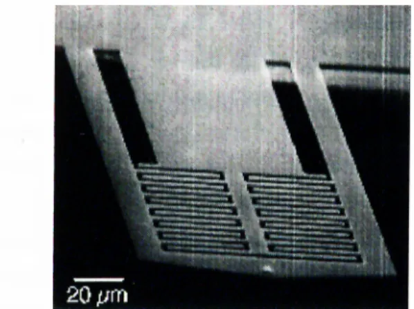
2.8 A 32 X 1 parallel AFM image of a lithographically patterned holes on a silicon substrate. Imaged area is 200 fan by 6.4 mm (512 pixels by 16384 pixels). Pixel size is around 0.4 /.im. The entire image area is 1.28 mm“^. 'Phe image rejiresents the horizontal combination of l.he 32 individual images. It has been broken into four strips, and offseted vertically, lor display purposes. The box in the bottom left of the image represents the maximum scan size of a typical AFM, 100 fim x 100 //m... 17 3.1 Geometry of (a) the first kind and (b) the second kind interdigital cantilever 19 3.2 SEM image of an interdigital cantilever. The length of the cantilever is
215 /im. The length and the width of the fingers are 30 /im and 3 /an, respectively. The thickness of the structure is 2.5 /im. The cantilever is
micro-fabricated in Ginzton Lab., Stanford. 20
3.3 The simulated first four mode shapes of the second kind cantilever. (Young modulus, F^=130 Pa, density, />=2.332 g/cm'^, Poisson ratio, <t=0.278) . . 20 3.4 Gross sectional view of the grating. The width of the fingers are 2 /an. 21 3.5 Field intensity at D=2cm. Fingers are assumed to be infinitely long, (x
in m e te r)... 22 3.6 Goordinate system... 24 3.7 (a) Cantilever pattern, (b) </(a;o, i/o ) ... ‘•^4 3.8 Calculated diffraction pattern 4 cm above the interdigital cantilever for
various deflections. The width and the spacing of the fingers are 3 /iin
(,/y=0.167 X 10^ m -i) 25
3.9 Intensities of the zeroth and first order modes... 26 3.10 Differential detector output. Experimental and calculated data. The
length of the cantilever is 215 /<m. Incidence angle is 20°... 27 4.1 Noise sources in a typical AFM system which uses optical detection methods. 29 4.2 Electrical equivalent noise circuit of Figure 4 . 1 ... 29 4.3 Lever detection m eth o d ... 31
4.4 Calculated SNR. and MDD of interdigital cantile\'er with one detector for various values of n;. ‘o’ shows optimum bias poijit. {P=\ rnVV, )R=0.54, 7г=0.9, 7гı=0.185, Q=100, k ^ l N t/m , /o=46 kHz, T '= 3 0 0 °K )... 34 4.5 Calculated SNR and MDD of interdigital cantilever with two detectors.
‘o’ shows optimum bias point. (T^o = 0.23, 7?.i = 0 .1 8 5 )... 34 4.6 Equivalent mechivnical noise amplitude due to I. shot noise current, II.
input noise current of op-amp. III. resistor .lohnson noise current, IV. input noise voltcige of op-amp... 36 4.7 Calculated SNR ratios of interdigital cantilever with two detector and
lever method. The quality factor of the cantilevers, Q, are 100. (For lever detection method; /=200 /im, a=15 /im .) ... 37 4.8 Positions of the laser spots on the split photodetectors for lever detection
method and interdigital cantilever with two detectors... 38 5.1 General n-port netw ork... 41 5.2 Analogy between mechanical systems and electrical circuits. 42 5.3 FEM modeling of a cantilever beam and the electrical model. The length
and the width of the cantilever is 100 /nn and 40 //,m, respectively, 'hhe thickness of the cantilever is 1 ¡.im. Cantilever material is silicon (Young modulus, E=130 Pa, density, p=2.332 g/cm^, Poi.s.son ratio, (7=0.278). Node M is in the middle of the free end... 15 5.4 Calculated RMS mechanical noise amplitude of the free end (node
M) of the cantilever by using FEM & Eqn. 5.15 (tempei'ature, 7\ is 300 K) {¡A = 100 Hz, Jb = 70 kHz, f c = 123 kHz, f o = 380 kHz, fpj = 768 kHz). 46
5.5 Calculated RMS mechanical noise amplitude along the cantilever axis at / — fA = 100 Hz and / = f c — 123 kHz. ‘o’ shows FE nodes, i
(nodes along the ca.ntilever axis). 47
5.6 Correlation coefficient between the nodes along the cantilever axis and the node at the middle of the free end, (node M ) ... 48
5.7 Correlation coefficient between the node at the free end (x=100 /an) and the nodes at x=.30 /¿nr, x=60 /mi, x=85 /mi for Q = 100 and Q = Í as a function of frequency... 49 5.8 The signal power when the cantilever is deflected by an applied force of
10 pN to the free end. Noise power is calculated foi· a bandwidth of 50 kHz. 50 5.9 Calculated signal to noise ratio (SNR) along the cantilever axis within a
bandwidth of 50 kHz when 10 pN signal force is applied to the free end. . 51 5.10 Interdigital cantilever and the form of correlation m atrix... 52 5.11 Correlation coefficient between node A and B... 52 5.12 Mode shapes of the fingers at different resonance frequencies. The finger
length is 120 /¿m... 53 5.13 Generic interferometer... 54 5.14 The Michelson interferometer... 55 5.15 ID cantilever and ordinary AFM cantilever illuminated l)y a circular laser
beam. The thickness of the ID cantilever is 1.0 /mi and the thickness of the other cantilever is 0.51 /mi. Shadowed elements have been used to calculate the total noise... 60 A.l Cantilever model. Adopted from reference [28]... 66
List of Tables
2.1 Rc -- 3000i). Cantilever clis.sipates 1 rnW. Bridge voltage, is 15 V. f show.s the most feasible combination... 11 -1.1 Calculated square of noise currents and equivalent rms mechaniccxl noise
amplitudes due to the various noise sources in different detection methods in 1 kHz bandwidth. Laser dependent noise sources are not considered. (n;=0, nps=0) Input noise current of the amplifier, < in >, is 2 pA/Hz^^^. Input noise voltage of the amplifier, < e„ >, is 10 nV/Hz^^^. The resistor
of the transimpedance amplifier is 10 KH. 36
5.1 Below resonance (100 Hz) and on resonance (123 kHz) RMS mechanical noise amplitudes calculated by using different methods... 47 5.2 Resonance frequencies between 0 and 300 kHz. for diflerent finger lengths. 54 B.l Noise currents in different detection methods, (n.z. : non-zero) 70
Chapter 1
INTRODUCTION
Scanning probe microscopes (SPMs) are a class of instruments used to mecisure cuid modify surface properties. Since their introduction to industry, SPMs have become the most popular tools in many fields as diverse as mai.erials science, semiconductor technology, biology, biochemistry, storage applications, lithography, etc. In the most common form of a SPM, a shiirp probe is brought close to the sample surface and the interaction of the probe and the surface is measured while the probe is scaniK'd over the surface.
The most widely used tool for imaging and measuring surface topology has lieen the optical microscope. The early forms of the instrument have been introduced by Hooke cuid Leeuwenhoek in 1600’s. Since its invention, researchers have continuously tried to improve the resolution of the device and today’s microscopes have reached the typical resolution limit set lyy the wavelength of the light they use (about 1 /.tin). Optical microscopes produce images of optically transiDarent or semi-transparent surfaces in the
X and y direction, on where surface lies, they cannot provide any measurements in the
direction normal (z) to the surface.
In 1926, Busch (German physicist, 1884-1973) demonstrated that a suitably shaped magnetic field could be used as a lens to create electron microscopes. In 1940’s, Ruska (German physicist, 1906-1988) and co-workers designed and 1)uilt the first practical scanning electron microscope (SEM) which surpasses the resolution of optical microscopes. Today, typical resolution for SEMs is about 50 k. Like optical microscopes, SEMs can only measure the x and y dimensions of the sainple.
Scanning probe microscopes are the newest entry into the surface imaging held. As opposed to optical microscopes and SEMs, they do measurement s in all three dimensions. The resolution in x — y direction is typically between 1 A a.nd 20 A and they can resolve features cis low as 0.01 Á in direction.
The first SPM which is introduced by Binnig (German physicist, 1947- ) and co workers was the scanning tunneling microscope (STM) [1] which makes use of strong dependence of tunneling current on the distance between tlie sharp probe and the sample surface. In STM systems, a sharpened, conducting tip is scanned across the sample surface with a bias voltage applied between the tip and the sample. When the tip sample distance is less than 10 Á, electrons tunnels through the gap. The tunneling current varies with the tip to sample spacing, and this signal is used to create STM images. STM was the first device to generate real-space images of surfaces with atomic resolution. One disadvantage of the STM is that both tip and the sample should be conducting.
Another kind of SPM is the atomic force microscope [2] (AFM) which has been originated from STM. Besides tunneling current, STM tip e.xerts force on the surface of the samples which has a magnitude on the order of interatomic forces. This effect gave rise to a novel instrument, atomic force microscojíe. Binnig and co-workers positioned the STM tip almost parallel to the sample surface so that its sharp edge is just above the surface. The tip, acting as a cantilever, exerted force to the sample surface and the deflection of the tip was measured by another STM tip. By displaying the deflection of the tip as function of the tip position atomic resolution image of the surface was obtained.
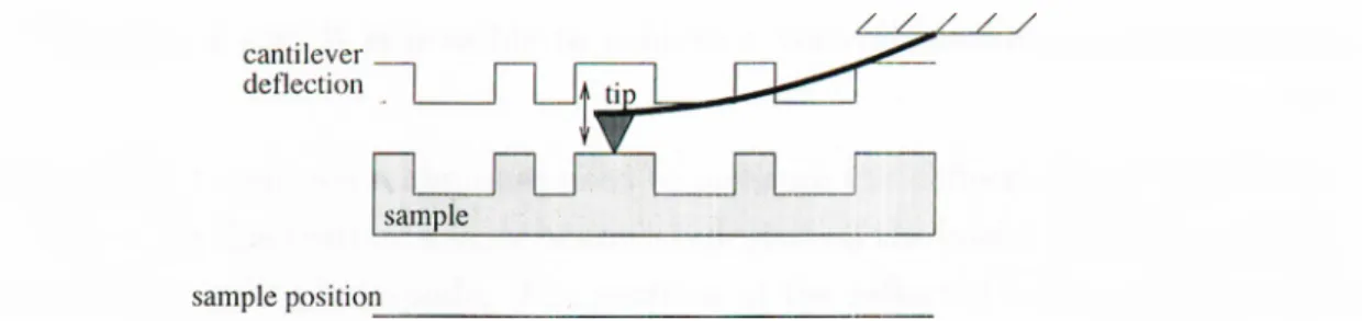
AFM provides high resolution topographic images of conducting and insula surfaces. As its name suggests, it measures forces between the atoms of the sharp tip and the sample surface. The most crucial jiarts of the AFM aie the spring cantilever beam with a very sharp tip attached at the one end of it and a cantilever deflection detection system. The cantilever tip is pressed into contact with the surface to be imaged. The atomic forces between the tip and the surface cause the cantilever to deflect which is measured by the deflection detection sensor. The cantilever is then scanned across the surface and the deflection of the cantilever is recorded at each pixel. Hence, the topographic image of the surface is obtained. This mode of operation is called as “constant height” mode, the sample height (distance between the sample and the tip) is not changed during the scan. The dynamical range of this microscope is limited by
Figure 1.1: Typical AFM sy.stem with Z-feedback.
the maximum allowable deflection of the cantilever. For tcill fea.tures, the force between the tip and the sample increases drastically, which may darna.ge the tip or the sample. In the other mode of operation, “constant force” mode, the distance hence the force between the tip and the sample is kept constant by changing the position of the sample. Deflection sensor detects the deflection and a controller unit adjusts the jrosition of the sample in the 5; direction as shown in Figure 1.1. Two modes of operation are depicted in Figures 1.2 and 1.3.
For the AFM systems, two kinds of resolution can be defined; spatial resolution and vertical resolution. The spatial resolution is determined by the maximum of the step size of the image and the radius of the tip end. Consider a 512 by 512 data points image of 1 /<m by 1 ;tim area. In this case, the spatial resolution is around 20
A
(1 //,m-f512) if the radius of the tip is less than 20A.
The diameter of the tip end is typically less than 50A
and these tips provide lateral resolution less than 10A.
With the best instruments and suitable samples 1A
resolution can be achieved.Pixel in AFM images is defined in the same manner as image processing systems. An AFM image is the discretized version of surface topography in both spatial coordinates and height. We may consider an AFM image as a matrix whose row and column indices identify a point on the surface and corresponding matrix element value identifies the height at that point.
Figure 1.2: Constant height mode of operation. Tip position hence the deflection of the cantilever changes according to the sample surface.
sensor. Various deflection detection schemas have been employed since the investigation of the AFM. The most common sensors include tunneling [2], interferometry [3, 4], the optical lever [.5, 6], and a piezoresistive element [7] used to sense the strain. The sensitivity with these methods is sufFicient to resolve features on the atomic scale and indeed this fine sensitivity is a basic factor in the widespread acceptance of the AFM.
One of the first techniques for measuring the deflection of the cantilever is an electron tunneling detector [2]. This is done by placing a tunneling electrode near the metal coated cantilever. The operation is similar to the scanning tunneling microscope. A bias voltage is applied between the electrode and the cantilever while tunneling current is measured. The current depends strongly on the distance between the electrode and the cantilever. Hence, by measuring the current, cantilever deflection is found. One disadvantage of this method is that both attraction and repulsion forces between the electrode and the cantilever can cause a considerable deflection of the cantilever.
A highly sensitive technique for measuring the deflection of a cantilever is the interferometer. Rugar et al. [4] developed a deflection sensor based on the interference of light between the cleiived end of an optical fiber and the backside of a cantilever. By accurately positioning the fiber above the cantilever to form a tightly sj^aced interference
cantilever deflection
sample position__[~
Figure 1.3: Constant force mode of operation. The sample position adjusted so that the tip position hence the cantilever deflection is kept constant.
cavity of less than 4 /im, it is possible to achieve a vertical resolution on the order of O.Of Ä.
One of the most common techniques used to measure the deflection of a cantilever is the optical lever. In this system, a laser beam is reflected off the backside of the cantilever and directed into a split photodiode. The position of the reflected beam, and hence the cantilever deflection, is determined by subtracting the photodiode outputs. Unlike the interferometer, the optical lever does not require the positioning of components directly above the cantilever. It is this simplicity that has made the optical lever more popular than the interferometer. However, the resolution is typically limited to roughly 0.1 A.
The deflection of a cantilever can also be determined with an integrcited piezoresistive strain gauge. Since silicon is a piezoresistive material, it can be used to microfabricate cantilevers that change resistance when stressed. Developed by Tortonese [7], the piezoresistive cantilever is capable of 0.1 Á resolution in a 10 Hz to 1 kHz bandwidth. The main advcintage of using a piezoresistor to measure cantilever deflection is that alignment is not required. In the case of the optical lever, there are typically two alignment steps that require physical positioning: first, a laser must be aligned to the end of the cantilever and second, a s25lit-photodiode must be aligned to the laser Iream that reflects off the cantilever. When using the piezoresistor, it is only necx^ssary to l)alance the resistor bridge by changing the resistance of one of the elements. For low temperature or UHV applications where i^hysical alignment is difficult, the piezoresistor is a simi)le alternative. The piezoresistor is also a useful techniciue for measuring the deflection of cantilever arrays [8]. .In chapter 2, piezoresistive detection technique will be described in details and driver electronics that we built for large array of cantilevers will be presented.
The advances in silicon micro-machining techniques permit us to fabricate cantilevers with intricate designs and small dimensions. Our new interferometric detection method, as introduced earlier in [9], is based on a cantilever shaped to form an interdigital optical diffraction grating. The interdigital grating is composed of two sets of fingers. One set contains the tij? which follows the contour of the sample. The other set is rigidly connected to the cantilever support and remains stationary during scanning. When the fingers are illuminated, the optical beams reflected from fingers produce a diffraction pattern composed of many orders. The intensities of each order depend on the amount of cantilever deflection. In this way the cantilever deflection is determined by a simple measurement of optical intensity and this gives us the simplification that is needed to adapt this system to cantilever arrays.
This thesis mainly cleixls with the analysis and the noise perfoniumce evaluation of the intercligital (ID) cantilevers. However, before the analysis of the ID cantilevers, one problem of the AFM systems will be pointed out. Although striking advances in the technology of AFM systems, one of the most crucial problems is the scan speed. The main limitations are due to the low speed of mechanical scanners and the low resonance frequencies of cantilevers. One possible solution to this problem is to operate more than one cantilever in parallel to increase the throughput of the system. In chapter 2, we will present a state of the art method for the cantilever arrays, which uses piezoelectricity. We will also demonstrate an electronics for a i^arallel AFM system which uses piezoelectric cantilevers and AFM images obtained by using this electronics.
In chapters 3 and 4, we present a detailed analysis of the operation of the interdigital (ID) cantilever. We will first introduce the geometry then formulate the theory underlying the operation of the phase gratings with the responses curves and confirming experimental results. The noise performances of the ID cantilever will be compared to the most popular deflection detection schema, optical lever detection method. Then, in chapter 5, we will present a novel method for the noise analysis of the mechcuiical structures by using similar techniques that are used in electrical circuits and the analysis method will be applied to AFM cantilevers and ID cantilevers. By using this method, noise correlation within a mechanical structure will be Ccilculated. We will also demonstrate the noise analysis of interferometric methods which also includes the noise correlation.
We will conclude with a discussion of the overall advantages of the ID cantilever, improvements of the array electronics.
Chapter 2
PARALLEL AFM WITH
INTEGRATED PIEZORESISTIVE
SENSOR AND ACTUATOR
AFM has proven itself as a. very promising tool for surface imaging since its invention. In spite of the advances in the technology of the devices, one common limitation of the AFM is the scan speed. Usually, imaging a 50x50 ¡.im area requires a few minutes. The problem is due to the serial nature of the single tip sccuming at relatively slow speeds. OiK' possiljle solution to increase the speed is to use array of cantilevers in parallel.
In typical AFM systems, deflection of the cantilever is monitored with an optical beam precisely aligned to the cantilever. But, it is difficult to apj)ly the same system for the cantilever-arrays, because of the increased alignment re(|uirements as the numbei· of cantilevers. This problem can be overcome by integrating the sensor into the cantilever. Much work has been done on microfabricated electro-medianical sensors. One of the most popular method for measuring the deflection is piezoresistive sensors integrated in· the cantilevers [7, 8]. Piezoresistive sensors do not only decrease the alignment requirements, but they also mahe possible to scan the cantilevers with respect to sample. Foi· AFM systems which use optical detection methods, alignments must be preserved while scanning. For this reason, most AFMs hold the cantilever and detection system fixed and scan the sample. As long as the sample is small this technic[ue is practical.
however there is growing interest in using the AI''M to i wafers cuicl rigid magnetic disks.
large samples like silicon
Integrating deflection detection sensor in the cantilever solves the parallel detection of deflection. For constant height mode of operation, by scanning an array of cantilevers with integrated sensors on the sample, a parallel innige of surface is easily obtained. However, for constant force mode of operation there is another difficulty. In single tip AFM case, usually sample is moved in the Z-direction to keep a constant force between the cantilever and the sample. To image the sample surface with an array of cantilevers in the constant force mode, each cantilever should have an independent actuator which is also integrated in the cantilever. Actuators consisting of ZnO film located at the cantilever base solves the problem of independent actuation [10] (Figure 2.1).
ZnO Electrode.s ZnO
Figure 2.1: Piezoresistive cantilever with integrated ZnO actuator
In this chapter, first we will present the theory of piezoresistive detection. Then, electronics for parallel cantilever arrays will be described. We will also present images obtained by using parallel AFM.
2.1
P iezoresistive sensing
Piezoresistive cantilevers make use of piezoresistive effect, which is known as the variation of. bulk resistivity with applied stress, to sense the cantilever deflection. Silicon is a piezoresistive material and it is very suitable for fabricating the cantilever beams. Piezoresistive cantilever is composed of two piezoresistor arm and a triangular part which holds the tip as shown in Figure 2.1. The value of piezoresistor changes with the tip displacement. The change in the piezoresistor is detected l)y a Wheatstone bridge (Figure 2.2).
Figure 2.2: Wheatstone bridge
The output voltage between the two terminals of the Wheatstone bridge, as a function of change in piezoresistor (AR) is given by
V ,, = 14 - 14 = Vl)ia.sARR2
{ R + R2){R3 + Rc)
When there is no deflection, {AR = 0), bridge should be l)cdanced,
R^Rc R2 _ R3
Ri Rc R3 Ri
Substituting, Eqn. 2.2 in Eqn. 2.1,
— ^bias f A R \ R Ji2
\ Rc / (Ri +
(2.1)
(2.2)
(2.3)
Now, assume that piezoresistor signal is amplified by an amplifier shown in Figure 2.3. The signal to noise ratio (SNR) at the output of the amplifier is given by.
SNR =
1/2
pzr
B{ilR^ + el + -ikeTR) ’ (2.4)
where R = R i / / R2 + R3IIRc and B is the detection bandwidth, in is the input noise current, e,i is the input noise voltage of the amplifier, ks is the Boltzmann constant, T is the temperature in Kelvin. By using Ecjn. 2.2,
R = R2(Ri + Rc)
+ R‘i (2.5)
hence, signal to noise ratio,
SNR =
T/·^ fA/lVV R,R2 Y
'htas{R,J
B{ilR^ + el + 4k.BTR) (2.6)
SNR at the output is directly proportional to the squan? of the bias voltage. It may seem advantageous to keep the bias voltage as high as possible. However, this increases the heat dissipated on the piezoresistor, causing the thermal drift to become a serious problem. Power dissipated on the cantilever should be kept within a few watts. Power dissipated on the cantilever is given by
2
Rc . (2.7)
Pc =
Again using Eqn. 2.2
HLs —
^¡>¿04· R 3 "h R c
PciRl + R2Y Rc
R?
(2.8)Typical resistance Vcilue for a piezoresistive cantilever is around 3 k {Rc — 30000) and the power dissipated on the cantilever should be kept less than 1 mW. If we assume that we use 15 V for the bridge, from Eqn. 2.8, we find that,
R2 = 7.66R1 (2.9)
If Eqn. 2.9 is substituted in Eqn. 2.6, the maximum value of Eqn. 2.6 is achieved when
Ri is zero and
SNR„.„. = 3.2763 X 10'"
(
4
. (2.10)\ R c J B '
Ri and i?2 should be kept as small as possible to achieve high SNR. However, there is a practical limit for these resistor which is set by the power dissipation. Typically, stiindard metal film resistors dissipate 0.25 Watts. If Ri = lOOO and R2 = 7660 then SNR=3.1310 X 10'" K. With this coniiguration /¿2 dissipates 0.23 Watts whidi is about the maximum allowable rate for standard 1/4 Watts resistor. SNRs for different Ri values are given in Table 2.1.
R\ — 0 & R2 — 0 Ri = 10 k R2 = 76.6 Ri = 100 k R2 = 766 ^ i?i = 1000 k R2 = 7660 SNR=.3.2763 X 10’® K SNR=.3.2611 X 10’® K SNR=3.1310 X 10’® K SNR=2.1793 X 10’® K
Tcible 2.1: Rc = 30000. Cantilever dissipate.s 1 rnW. Bridge voltage, Vua.,. is 1.6 V. t shows the most feasible combination.
2.2
C antilever-array electronics
Cantilevers with integrated piezoresistive detection and actuation are the heart of the pcuallel AFM system. However, they are not enough for parallel atomic imaging. Parallel imaging by using cantilever arrays requires individual detection and actuation of each cantilever with a sej^arate electronic circuit.
The need for high speed imaging is steadily increasing. It is accepted that single AFM cantilevers will not achieve data rates useful for industry. For example, only arrays of 1000 or more could achieve rates comparable to those of magnetic disks [11]. With the help of micromachining, laj-ge number of cantilevers ca,n be brought together in a lew centimeters. However, for such arrays, the size of driving electronics is becoming larger and larger.
For small arrays of cantilevers it is possible to manually control all aspects of the cantilever’s ojseration during an imaging experiment. However, for massively parallel operations, or operation in a scalable system, it is important to have a compact electronic system for automated control. In the piezoresistive/ZnO system, the position of the cantilever arm is detected by microvolt changes in the piezoresistive sensor’s bridge circuit. This voltage is cimplified to tens of volts to generate a. suitable signal for feedback and analysis. Since the voltage gain is high, special considerations need to be given to electronic noise and phase delays in order to create a high-speed, sensitive, electronic system. Automation is achieved through computer control of the microscope’s oj^erational parameters: force setpoint, gain and feedback.
The specifications of the electronics for AP’M arrays can be summarized as follows, • High density, small area: To support large number of cantilevers, electronic
components should fit in an area as small as possible, 'hhis can be achieved by 11
using integrated circuits, surface mount and multi layered printed circuit Ijoard (P (J B ) technology.
• lx)w noise, high gain-bandwidth product; The resolution of an AFM is determined by the noise level of the system. Theoretically, piezoresistor and 3 resistor in the Wheatstone bridge determines the noise floor. Noise contribution of the electronic circuit should be as low as possible. For high imaging bandwidth, electronic circuit should not introduce too much phase shift.
• Computer controlled: It is a very tedious work to balance all bridges with potentiometers separately. Instead of this, bridges should be balanced by a computer. The computer also sets the gain of each feedback loop.
• High speed computer interface: Images from cantilevers should be displayed on a computer monitor in real time. For large arrays, data flow rcite from cantilevers to computer memory is limited by the speed of computer interface.
We designed and assembled such a PCB for an array of 16 cantilevers^. Figure 2.4 shows the photographic image of the PCB. Each PCB has 16 channels and they are installed in a. computer on ISA bus. The number of PCBs that are working in parallel is limited bj^ the number of ISA slots in the computer. With a typical number of 4 slots, 64 cantilevers can work in parallel.
Figure 2.5 depicts electronics for an individual cantilever with integrated piezoresis tive sensor and piezoelectric actuator. Piezoresistor forms one arm of the Wheatstone bridge. Output signal from the bridge is amplified by a differential preamplifier (Ci). Preamliher is chosen so that it has very low input noise voltage (e,i = l^inV/s/Hz) and noise current (i„ = 2pA./\fHz) while maintaining the highest liandwidth. Piezoresistor signed is further amplified ( C 3 ) by using wide bandwidth amjjliiiers. The gain ((¡2) of the
hrst stage is controlled by the computer. Integrator enables integral control. The integral of the piezoresistor signal is then applied to ZnO films by a high voltage amplifier. ZnO films can bend the cantilever 4 /mi for voltages of ±35 V. This dynamic range is enough for atomic resolution imaging for constant force mode of o]ieration. The bandwidth of the amplifier chain is measured to be l.I MHz and the jihase shift at 100 kHz is less
10°.
hJuiTently, these boards are being used at Ginzton Lab., .Stanford, for one-dimensional array of :32 cantilevers and for two-dimensional array of -5x5 cantilevers at IBM Zurich Research Lab.
Figure 2.4: Photograi^hic image of PCB
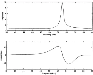
Figure 2.6 shows the response of one of the channels with a cantilever out of contact with the sample. The cantilever is attached to the bridge. A sinusoidal voltage is applied to the ZnO actuators and the voltage at the output of the high voltage amplifier is measured. Frequency is scanned from 40 kHz to 60 kHz. The voltage gain of the channel is set to 5000 (74 dB). The resonance of the cantihn^er is observed clearly at 52.5
э σο/ 6 to Ol g O rD < 2 ■:;Tî O c o’ Z n O Z n O / \
kHz. The quality factor is around 100. Note that this is not a closed loop rneasurenient.
Figure 2.6: Response of the driver electronics with a cantihwer connected to one of the channels. Cantilever is not in contact with the sample. A sine wave is applied to the ZnO films and the output signal from the high voltage a.mplifier is measured.
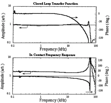
Figure 2.7 shows the closed-loop transfer function and th(i open-loop transfer function when the cantilever is in contact with the sample. CHosed-loop transfer function is obtained by adding a small sinusoidal signal to the amplifi(n· with gain 63 and measuring the amplitude and phase of the ZnO signal (output of the high voltage amplifier). The bandwidth of the system using a 40° phase margin is 20 kHz. Above this freciuency, phase shift in the system easily adds up to 180° which results in instability in feedback loop. The main limitation on bandwidth is due to the resonance of the cantilever. In contact open-loop measurement is done like non-cbntact measurement. Again, a sinusoidal voltage is applied to the ZnO layers and the ZnO signal is measured. When the cantilever is in contact, resonance frequency slightly increases to 60 kHz. (52.5 kHz when out of contact).
Figure 2.8 is a image of 200 /mi by 6.4 mm area and is taken with the parallel operation of 32 cantilevers. The real aspect ratio of the image is difficult to show, so the composite has been broken into four parts and separated in the vertical direction. Sample is a silicon substrate with lithographically patterned holes on it. The depth of the holes is 225 nm. The cantilevers were driven with Iwo 16-channel PC expansion boards that control the array’s operation, gain, and offset. Eacli cantilever scans an area of 200 /un by 200 /an on a grid of 512 by 512 pixels. Conventional piezotubes cannot be
b£) OJ»
T3
M
a.
Figure 2.7: Closed-loop transfer function and oj^en-loop transfer function of the cantilever in contcict with a sample.
used for this type of scanning because their typical range is much less than 200 fim. More importantly, the nonlinear z coupling of the piezotube ¡prevents linear scanning over a large area. To solve this problem a custom flexure scanner from Nikon is used for .r-scan (fast scan direction) and it is driven by a sinusoidal voltage instead of a triangular wave to decrease the mechanical oscillations of the scanner. After the image is acc|uired, it is deconvolved with a sine wave to obtciin the original image. Foi· the ?/-scan (slow scan direction) long range high resolution scanner from Newport (PM-500) is employed. The .I'-scan speed is 7.8 Hz and whole image takes 1 minute to acquire.
In Figure 2.8, the cantilever.s with numbers 5, 6, 7, 24 and 31 are broken. Black stains on images 4, 15 and 29 are probably caused by dust |)articles. The blurred image from the 16th cantilever is due to the blunted tip of the cantilever. VVe believe that this image represents the largest parallel probe operation to date (Lutwyche and co-workers have achieved to operate 5x5 array of piezoresistive cantilevers [11]).
Figure 2.8: A 32 x 1 pcvrallel AFM image of a lithographically patterned holes on a silicon substrate. Imaged area is 200 /¿m by 6.4 mm (512 pixels by 16384 pixels). Pixel size is ciround 0.4 ¡nn. The entire image area is 1.28 mnP. The image represents the horizontal combination of the 32 individual images. It has been broken into four strips, and offseted vertically, for display purposes. The box in the bottom left of the image represents the maximum scan size of a typical AFM, 100 ¡im x 100 //m.
Chapter 3
INTERDIGITAL CANTILEVER
Micro-machinecl diffraction gratings have been used in many micro-optical systems [12, 13]. Integrating a diffraction grating onto the cantilever is capable of sub-angstrom resolution in AFM. The principle of operation is very simple. Optical grating is compo,sed of two sets of fingers. One set, called as “moving fingers”, is connected to the tip and moves cvccording to the surface topography of the sample that is scanned. Other set, called as “reference fingers”, remains fixed. If the cantilever is illuminated by a coherent light source, the fingers form a phase sensitive diffraction grating, and the tip displacement is determined by measuring the intensity of the diffracted modes.
3.1
G eom etry
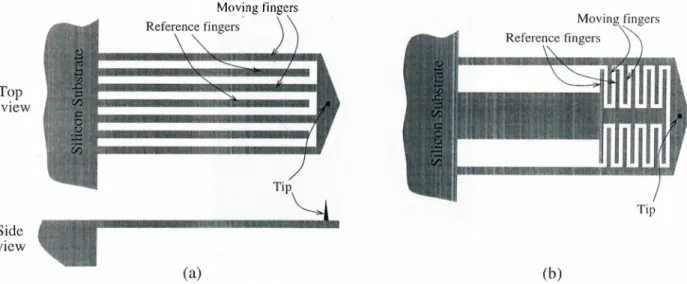
There are two wa.ys of implementing jDhase gratings on cantilevers. Figure 3.1a shows the first kind cantilever where the fingers are directed along the direction of the cantilever axis. In the second kind the fingers are perpendicular to cantilever axis (Figure 3.1b). There is little difference between two geometries except foi' the diffraction pattern which is perpendicular to the cantilever for the first kind and parallel to the cantilever axis for the second kind. The geometry of the first kind is more simple in some ways, but it is not suitable for arrays since the higher order diffraction patterns from neighboring cantilevers interfere with each other.
The typical ID cantilever is several micrometers thick, several hundred micrometers 18
Moving fingers
(b)
Figure 3.1; Geometry of (a) the first kind and (b) the second kind interdigital cantilever in length and 100 micrometers in width. A sharp tip perpendicular to this surface is formed at the end. The cantilever is fabricated from silicon with the standard techniques of micro-nicichining. Alternatively, silicon nitride can be used in place of silicon and the surface of the fingers are coated with an optically reflecting material such as aluminum or gold.
A scarming electron micrograph of the ID cantilever of the second kind is shown in Figure 3.2. The tip is visible on the triangular piece at the end of the cantilever. One set of fingers is connected to the outer portion of the cantilever which moves when a force is applied to the tip. The second set of fingers is connected to the inner portion which remains fi.xed.
We have used a. general purpose finite-element pcickage, ANSYS version 5.2 [14], to study the shape of the modes and the associated resorumces. A 4-node elastic shell element (SHELL63) was used to construct the FEM model, 'riiis resonance is important since the high frequency limit of the imaging bandwidth is set by the first resonance peak of the cantilever. The calculated and experimentally measured resonance frequency of our cantilever is around 46 kHz. This is the first longitudinal resonance of the outer portion of the Ccintilever. Figure 3.3a shows the mode shape for the first resonance. At this frequency, triangular part of the cantilever moves up and down. The second resonance frequency is the first longitudinal resonance of the inner part (Figure 3.3b). The third mode corresponds to a torsional mode where the cantilever rotates around the axis of the cantilever (Figure 3.3c). The individual fingers resonate at a frequency above
í ’igure 3.2: SEM image of an intercligital cantilever. The lengtli of the cantilever is 2L5 /mi. The length and the width of the fingers are 30 /mi and 3 /mi, respectively. The thickness of the structure is 2..5 /¿m. The cantilever is micro-fabricated in Ginzton Lab., Stanford.
3 MHz.
3.2
T heory o f phase gratings
The geometry of the interdigital cantilever forms a phase sensitive optical diffraction grating. This grating reflects the incident coherent optical beam into several orders
(a) f,=46.3 kHz (b) r,=98.8 kHz
(c) f,=182.6 kHz (d) r,=293.6 kHz
Figure 3.3: The simulated first four mode shapes of the se;cond kind cantilever. (Young modulus, .£=130 Pa, density, p=2.332 g/cni^, Poisson ratio, <7=0.278)
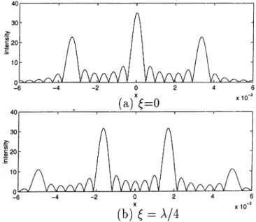
with an intensity that depends on the rehitive disi^lacernent between tlie two sets of fingers. Figure 3.4 shows the cross section of the grating and the profile of the optical diffraction pattern. In the equilibrium position, ^ = 0, where ( represents the relative deflection of moving fingers with respect to reference fingers, the intensities of the even- numbered orders are maximum (P’igure 3.5a). The spatial separation of the second order component from the central component (the zeroth order) is XDfg, where fg is the spatial frequency of the grating, D is the observation distance and A is the wavelength of the incident beam. When the moving fingers are displaced by A/4, the central beam vanishes and the energy is divided between two first order components and other odd numbered components (Figure 3.5b). Figure 3.5 was calculated from fingers of infinite length. The diffraction pattern profile is calcidated by taking the one dimensional Fourier transform of the grating. If we assume the amplitude of the incident l)earn varies ¿is cos(u)t + kz), where k — 2tt/ \ is the wavenumber, we can calculate the intensity of the zeroth order
component as a function of cantilever deflection. At ^ = 0 the amplitudes of the beam reflected from the two sets of fingers are cos(ujt) and cos(u;¿ -j- 2k.^), respectively. If we add these two cosine terms, we find that the intensity of the zeroth order component, 7o, is proportional to /ooccos^d, (3.1) 3. - 6 m m 2. - 4 m m - 2 m m orders 0. O m m 2 m m 4 m m
Figure 3.4: Cross sectional view of the grating. The width of the fingers are 2 /¿m.
wher;e
27T
(3.2) The reflected beams from moving fingers and reference fingers add constructivel_y when if = 0, A/2, A, 3A/2... Similarly, the intensity of the first order component, ./j, is proportional to
/1 oc sin^ d . (3.3)
Again, reflected beams from moving fingers and reference fingers add constructively when f = A/4, 3A/4, 5A/4... The phase difference between incideiit and reflected bea.m is 2A:f when we assume that incident beam is normcil to the cantilever plane, i.e. incidence angle is zero degree. Experimentally, it is difficult to illuminate the cantilever with this angle of incidence and measure the diffraction pattern at the same time since there is usually a small incidence angle, 7. If the effect of incidence angle is considered, in above formulae, f should be replaced by f e o s7. We note that we maximize the sensitivity when the incidence angle is kept as small as possible.
Another issue that must be considered when designing interdigital cantilevers is the spatial separation of the orders. If the orders are not well separated, they interfere with each other and this reduces sensitivity. The beam width for an order at the observation plane is proportional to XDfgfN^ where N is the number of finger pairs and N / fg is the length of the grating. The ratio of the spatial separation between successive orders to
Figure 3.5: B'ield intensity at D=2cm. Fingers are assumed to be infinitely long, (x in meter)
the beam width [15] can be considered as a figure of merit and it is given by
f , \ D / 2
\ D f j N = N/2 . (3.4)
This ratio is proportional to the number of fingers, but it is independent of observation distance D. We conclude that for N is greater than 4, the orders are well-se|)arated.
3,3
Two dim ensional analysis and experim en tal
results
In order to simulate the performance of the interdigital cantilever, the diffraction pcittern above the interdigitated fingers has to be determined. The difli’action pattern from an arbitrary source distribution can be found by using well-known diAhaction integral [16] which can be difficult to calculate. However, Fresnel approximations for near field calculations is very accurate and computationally less complex. The Fresnel formula for calculating field amplitude due to an arbitrary source distribution is given by the Fourier transform of the source distribution multiplied by a constant ]rhase surface. With the nota.tion defined in Figure 3.6, the resulting field, u{xi,yi), due to an arbitrary source distribution, g{xo, yo), is given by
1
where
//(//,., lyy) = F < g{xo, yo)e so
(3.5)
(3.6) The light intensity a,t z = D plane is ¡Droportional to )ii(;i·], ;(/i)]^. Hence, the intensity is
{DXy
2 7 T X 1 __ 2TTV/J A D ' ' ' y - A D
(3.7)
The intensity is calculated from the two dimensional fast Fourier transform. In Figure 3.7a, we show the intensity distribution at the cantilever plane, = 0. In general the displacement ^ is a function of .tq and yo and it is denoted by ^(xo. yo)· The amplitudes of the moving parts are multiplied by a phase term, exp(47rj^(,ro,;yo)/^)i which denotes the additional two-way phase difference due to the cantilever deflection.
Cantilever plane Detector plane
Figure 3.6: Coordinate system.
^(.To,i/o)· When a force is applied to the tip, the deflection of the cantilever varies along the length of the cantilever. It is zero cit the jDoint where the cantilever is connected to the silicon substrate and maximum at the tip. The cantilever deflection, 2/o), is calculated as a function of xq and yo by using ANSYS. fl’he tip is deflected by 210 nm
with a force of 23 nN on the tip. The calculated spring constcint of the Ccintilever is
1.1 Nt/rn.
The function g{xo,yo) is obtained by weighing the cantilever pattern by a Gaussian beam, exp( —(a;Q + ?/o)/'^^)» where <r = 3.6 /irn (Figure 3.7b). Once y(.To, yo) is determined, the intensity pattern at the desired z = D plane is found by applying the Ecjn. 3.7. In Figure 3.8, we show the calculated diffraction pattern for various cantilever deflections.
(a) (b)
Figure 3.7: (a) Cantilever pattern. (b)y(a:o,yo)
With no deflection i^{xo,yo) = 0), the intensities of the even-numbered orders are maximum, for D = 4 cm, the spatial separation of the second side order from the central component is 4.46 mm as calculated from XDfg. This value is consistent with Figure 3.8. When the cantilever is deflected 210 nm, intensities of the odd-numbered components reach their maximum values. The distance between the first order component and the
x10"'
I
I
2 .1.
O pL·0. CD
1
.
2
.3.
-1 0 1 X 10'· X(m.)
^ : Onm
52nm
87nm
140nm
175nm
210nm
Figure 3.8: Calculcvted diffraction pattern 4 cm above the interdigitai cantilever for varioius deflections. The width and the spacing of the fingers are 3 /mi (/;,=0.167 X 10® rn"^)
zeroth order component is around 2.2 mm which is nearly A D /',/2.
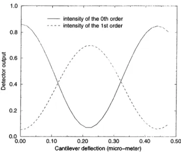
The cantilever deflection can be determined b}^ measuring the intensity of the zeroth order component, the first order component or the difference between the two. This is easily done by placing a photo detector at the proper position. Figure 3.9 shows the calculated detector output voltages versus cantilever deflection. For the detector output, we integrate over the area, corresponding to the size of the photodetector. The period of the curve is slightly larger than the expected value A/2. This is due to the fact that, the actual average displacement of the interdigital fingers is less than the displacement of the tip.
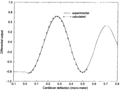
Figure 3.10 shows an experimental and calculated response curves. In the
Cantilever deflection (micro-meter)
Figure 3.9: Intensities of the zeroth arid first order modes.
experiment*, the interdigital cantilever of the second kind is illuminated by a laser beam with a spot size of 20 ¡J,m (a - 3.6^im) and the reflected diffraction pattern is measured with a split photodiode. The photodiode is placed so that zeroth order mode illuminates one side and the first order mode illuminates the other. The calculated curve is the difference of the two curves in Figure 3.9. The effect of incidence angle is also included. There is good agreement between the experimental curd calculated data.
* Experiments were done by a co-worker in Ginzton Lab., Stanford.
Figure ЗЛО: Differential detector output. Experimental and calculated data. The length of the cantilever is 215 fim. Incidence angle is 20°.
Chapter 4
COMPARATIVE NOISE
ANALYSIS
The sensitivities of all deflection detection techniques are limited by noise, l b compare the performances of different detection methods, signal to noise ratio should l:>e calculated. In this chapter, first, noise sources in a typical AFM system which employs optical deflection detection method will be discussed, then the noise analysis of the interdigital cantilever will be presented with a comparison l.o optical lever detection method.
4.1
D efinitions
The vertical resolution of the AF'M is determined by the minimum detectable deflection (MOD) of the cantilever. MDD is assumed to occur when signed power is equal to the noise power. Another term' which is useful while compaTing detection systems is sensitivity. In AFM systems, which use optical detection methods, the sensitivity, 5, of the system is defined a.S the output signal current generated by the photoddector per unit displacement of the cantilever and it is given by
dis
“ d^ ’ (T i:
- Thermal meclianical noise of the overall system Transimpedance Amplifier Laser
- Laser Intensity noise - Laser phase noise - Laser pointing noise - Laser 1/f noise
- Resistor Johnson noise - Blectrical 1/f noise - Electronic noise Cantilever
- Thermal mechanical noise of the cantilever
Figure 4.1: Noise sources in a typiccil AFM system which uses optical detection methods. where is is the signal current and ^ is the cantilever deflection. The main sources of noise in the deflection detection systems are shot noise of the photodetector, thermal mechanical noise of the cantilever, laser intensity noise, laser phase noise, laser 1/f noise, laser pointing noise, resistor .Johnson noise, electronic noise of the detection electronics and mechanical vibrations of the overall system (Fig. 4.1). Figure 4.2 shows the equivalent noise circuit. The signal is denoted b}' a current source of value is which is a function of the light intensity incident on the photo detector. The definitions and the symbols of the noise currents will be given in Appendix A. If the signal and noise powers from various sources are calculated from the circuit shown in Figure 4.2, the signal to noise ratio (SNR) is found as
where SNR = < Kk > + < t i > + < > + < i f > + < ti > < il > - < *L > + < ilha > + < ? : > + < > , (4.2) (4.3) Cantilever Overall mechanical system
Signal Detector Laser Circuitry
Figure 4.2: Electrical equivalent noise circuit of Figure 4.1 29
and
< > = < il > < et > . < + 4 > < 'i % > (4.4) Note that, for the purposes of calculating the signal power, the derivative of tlie output current is used rather than the current itself. For the SNR. calculation, the signal is defined as the change in the output current of the photodetector per unit displacement in the cantilever position. Our definition of the SNR, which includes the sensitivity of the system, is more suitable for AFM applications where displacements are small.
For a given SNR, the MOD of the system is easily calculated by using
1
MDD =
v / ^ ■ (4.5)
4.2
S N R for lever d etection
Assume that a cantilever as depicted in Figure 4.3 is illuminated by a laser beam and the reflected Iream is collected by a split photodetector. If the beam reflects from a square mirror with dimensions 2a by 2a, the profile of the beam at the photodetector plane is a square area with dimensions 2d by 2d where d is [16]
7T a
The optical power incident on each part of the split photodetector is
U P Pi = and P2 = R P (4.6) (4.7) (4.8) where P is the total power which is assumed to be incident on the square mirror with reflectivity R. The change of the position of the laser beam at the photodetector plane, óf/, is related to the cantilever deflection by
(4.9) Signal is the difference in the output currents of a split photodetector as in Figure 1.3 and it is given by [17]
i, = K ( a - a ) = , h = m p . (4.10) 30
Incident
Positions of ktser spots at detector plane
Figure 4.3: Lever detection method
where 5R is the responsivit}^ of tlie photodetector. The signal current is linearly dependent on the the Ccintilever deflection. The sensitivity of the optical lever method is e.xpressed as
chi
d^ XI
The sensitivity of the lever detection method does not depend on the distance between the cantilever plane and the detector unless the detectoi· is in the near field of the cantilever. The diffraction focal length of the beam is calculated by (2a)^/A which is typically a few millimeters. After this point, the beam diverges and the change of the laser spot position on the photodetector plane relative to its area remains the same, idence, placing a photodetector far from the cantilever does not increase the sensitivity of the system. Furthermore, the sensitivity is inversely proportional to the cantilever length. Decreasing the length increases the sensitivity at the expense of increasing the cantilever stiffness.
We next consider the effects of various noise components. To calculate the total mean square shot noise current, the shot noise powers at tlie each photodetector should be added. Hence, the total mean square shot noise current is given by
< i,\ > = 2qBI, (4.12)
Another noise source is the mechanical vibrations of the thermally excited cantilever. The mean square current due to the thermal vibrations of cantilever is
s f C >-Sn ^
\ XI
J
< C > ■ (4.13)where < > is the mean square thermal mechanical vibration amplitiicle of the
cantilever. If the above equations for signal and noise currents are sul^stituted in Eqn. 4.2, the resulting SNR formula for the lever detection method is
s f ! < ilk >
SNR/ei)ft7· — (4.14)
1 + S'l < e» > / < ''s/i > > / < ñh >
T’his equation is consistent with the equation given in rcrfereiice [5]. In reference [o], SNR. fonnula depends on the cantilever deflection wherea.s our formula does not. This is because we define the signal to be the derivative of the output current. Moreover, our SNR equation includes other noise sources. The theniial inechanical vibrations of the split photodetector witli respect to the cantilever as well as the vibrations of the laser with respect to the cantilever contribute to the overall mechcuiical system noise, contains contributions of the laser pointing noise and the mechanical system noise.
^'ps
The optical lever detection method can not distinguish the laser pointing noise in the direction normal to the split detector slit from the cantilever motion. The effect of the mechanical system noise is the same as the pointing noise, lienee, both noise components are combined in one variable nps (See Appendix B).
4.3
S N R for ID cantilever w ith one detector
The deflection of an interdigital cantilever can be determined by measuring either the intensity of the zeroth order component or the first order component. Let us assume that a photodetector is placed at the position of the first ord(?r beam and the deflection of the interdigital cantilever is determined by measuring the output current of tlie detector. By using Eqn. 3.3, the detector current can be written as
is — IiTZi sin^ 0 , (4.15) where TZi shows the ratio of the first order component power to the total power when the moving fingers are deflected by A/4. The sensitivity is given by
dT 2tt
SiDi = 7 7 = d<^ IT A ·
The maximum sensitivity is achieved, when the cantilever is deflected by A/8.
(4.16)
If Eqn. 4.15 is substituted in the shot noise current formula, the mean square shot noise current is
. (4.17)