Near-Unity E
fficiency Energy Transfer from
Colloidal Semiconductor Quantum Wells of
CdSe/CdS Nanoplatelets to a Monolayer of
MoS
2
Nima Taghipour,
†Pedro Ludwig Hernandez Martinez,
†,‡Ayberk Ozden,
§Murat Olutas,
†,⊥Didem Dede,
†Kivanc Gungor,
†Onur Erdem,
†Nihan Kosku Perkgoz,
∥and Hilmi Volkan Demir
*
,†,‡†Department of Electrical and Electronics Engineering, Department of Physics, UNAM-Institute of Materials Science and
Nanotechnology, Bilkent University, Ankara 06800, Turkey
‡Luminous! Center of Excellence for Semiconductor Lighting and Displays, School of Electrical and Electronic Engineering, School
of Physical and Materials Sciences, School of Materials Science and Nanotechnology, Nanyang Technological University, Singapore 639798, Singapore
§Department of Materials Science and Engineering, Faculty of Engineering, Anadolu University, 26555 Eskisehir, Turkey ⊥Department of Physics, Abant Izzet Baysal University, Bolu 14030, Turkey
∥Department of Electrical and Electronics Engineering, Faculty of Engineering, Anadolu University, 26555 Eskisehir, Turkey
*
S Supporting InformationABSTRACT: A hybrid structure of the quasi-2D colloidal semiconductor quantum wells assembled with a single layer of 2D transition metal dichalcogenides offers the possibility of highly strong dipole-to-dipole coupling, which may enable extraordinary levels of efficiency in Förster resonance energy transfer (FRET). Here, we show ultra-high-efficiency FRET from the ensemble thin films of CdSe/CdS nanoplatelets (NPLs) to a MoS2 monolayer.
From time-resolved fluorescence spectroscopy, we ob-served the suppression of the photoluminescence of the NPLs corresponding to the total rate of energy transfer
from∼0.4 to 268 ns−1. Using an Al2O3separating layer between CdSe/CdS and MoS2with thickness tuned from 5 to 1
nm, we found that FRET takes place 7- to 88-fold faster than the Auger recombination in CdSe-based NPLs. Our measurements reveal that the FRET rate scales down withd−2for the donor of CdSe/CdS NPLs and the acceptor of the MoS2monolayer,d being the center-to-center distance between this FRET pair. A full electromagnetic model explains the
behavior of thisd−2system. This scaling arises from the delocalization of the dipolefields in the ensemble thin film of the NPLs and full distribution of the electricfield across the layer of MoS2. Thisd−2dependency results in an extraordinarily
long Förster radius of ∼33 nm.
KEYWORDS: semiconductor nanocrystals, colloidal nanoplatelets, molybdenum disulfide, FRET, distance dependency, Förster radius, Auger recombination
T
wo-dimensional (2D) materials, also known as van der Waals materials, show diverse electronic structures and properties. Among them are examples of transition metal dichalcogenide (TMDC) semiconductors (e.g., molyb-denum disulfide, MoS2),1
semimetals (e.g., graphene),2 and insulators (e.g., hexagonal boron nitride, hBN).1 Specifically, semiconducting TMDC 2D crystals including MoS2and WSe2 exhibit very strong light−matter interaction.3
For instance, a MoS2 monolayer can absorb as much as 10% of the normal
incidence light at its excitonic peaks (615 and 660 nm).1,2This
strong optical interaction has attracted great attention for applications in optoelectronics,3−5 nanophotonics,2,5 and sensing.6−8 More recently, another important class of semi-conductors with their quasi-2D structure, colloidal quantum wells (CQWs), the so-called nanoplateletes (NPLs), which are most commonly synthesized in the form of CdX (where X Received: May 31, 2018
Accepted: July 2, 2018
Published: July 2, 2018
Article
www.acsnano.org Cite This:ACS Nano 2018, 12, 8547−8554
Downloaded via BILKENT UNIV on February 26, 2019 at 14:13:30 (UTC).
represents S, Se, and Te), have attracted interest for the ability to precisely control their vertical thickness.9−11Owing to the strong quantum confinement in the vertical direction, these semiconductor NPLs demonstrate attractive optical properties including giant oscillator strength and narrow photolumines-cence (PL) emission (purely homogeneous broadening).11−14 These interesting properties of the NPLs make them a highly promising material platform for efficient light-emitting diodes (LEDs),15lasers,11,12and photovoltaic devices.16,17
Nonradiative energy transfer (NRET) is an electromagnetic process of the energy transfer from a donor to an acceptor by near-field dipole−dipole coupling. One type of NRET is Förster resonance energy transfer (FRET),18,19
where the rate of the excitation energy transfer essentially depends on the distance between the donor and the acceptor as well as the spectral overlap between the PL spectrum of the donor and the optical absorption spectrum of the acceptor, the absorption cross-section of the acceptor, PL quantum yield (QY) of the donor, and orientation of the dipoles between the donor and the acceptor.18−20 The FRET process has been shown to
effectively enhance the performance of the light-generation, -harvesting, and -sensing functions in specially designed hybrid structures. To date, numerous FRET studies have been conducted using colloidal semiconductor nanocrystals with different degrees of quantum confinement (quantum dots (QDs), nanorods (NRs), NPLs).20 For example, FRET has been investigated in a hybrid structure of two types of NPLs, each with a different vertical thickness.21,22 Thanks to their large absorption cross-section, NPLs emerged as a highly promising candidate for absorbing photons and photogenerat-ing excitons potentially to be transferred via FRET. To this end, graphene,23,24 graphene oxide,25,26 and carbon nano-tubes27have been used as a sinking medium of the excitons. Especially, TMDC semiconductors including MoS228,29 and MoSe230have exhibited high capability of exciton sinking from neighboring nanoemitters. For example, the FRET pairs of CdSe/CdS QD-donors with MoSe2-acceptors
30
and of CdSe/ CdS QD-donors with graphene-acceptors,31which are shown to exhibit the distance scaling of d−4, have previously been reported. However, to the best of our knowledge, FRET has Figure 1. (a) Graphical illustration of the hybrid assembledfilms of NPLs−Al2O3−MoS2(donor−spacer−acceptor) system. (b) Schematic
representation of the FRET process where the energy band diagram indicates the transfer of excitons. (c) Normalized photoluminescence of the 4 ML CdSe/CdS core/crown NPLs (donor) and UV−vis absorption spectrum of the MoS2triangular monolayerflakes (acceptor). (d)
High-angle annular darkfield transmission microscopy image of the NPLs. (e) Scanning electron microscopy image of the MoS2film. (f)
Raman spectrum of the MoS2film. The inset shows the A1g− E2g1 central map of Raman spectra. (g) PL spectrum of the MoS2film. The inset
exhibits the spatial map of the exciton peak around 1.83 eV.
not been explored in the hybrid structure of the 2D NPLs and TMDCs, although such a combination is very favorable because of their intrinsic geometrical similarity. Owing to their atomically flat topologies, the layer-to-layer dipole−dipole interaction between NPLs and TMDC films would be expected to achieve ultraefficient FRET compared to any other possible combinations of nanocrystal semiconductors and 2D materials.
In the present study, we report FRET from solid assembled thinfilms of colloidal CdSe/CdS core/crown NPLs serving as the donor to a single layer of MoS2 serving as the acceptor.
Here, we systematically study the FRET process and surprisinglyfind the rate of the FRET decays as 1/d2, where
d is the distance between the donor NPL and acceptor TMDC 2D structures. Although the decay rate is expected to scale with 1/d4, we reveal that the strongfield screening and the dipole electricfield delocalization at the donor play a major role in modifying the decay kinetics. To study systematically FRET as a function of the distance between the NPL nanoemitters and MoS2monolayer, we deposited thinfilms of dielectric spacers
of alumina (Al2O3) with tuned thicknesses between the donor
and the acceptor precisely controlled using atomic layer deposition (ALD) and employed time-resolved fluorescence (TRF) spectroscopy to investigate the resulting luminescence decays of the NPLs. According to the measurements, the PL curves of the NPLs were significantly accelerated with decreasing thickness of Al2O3, which convincingly indicates the existence of the energy transfer. Subsequently, we found that by decreasing the spacer thickness to 1 nm, we achieved a near-unity energy transfer efficiency of 99.88% with an ultrafast
FRET lifetime of 3.73 ps at room temperature. Additionally, we support ourfindings with a full numerical electromagnetic model of the hybrid structure by simulating the dipole interaction within the model structure. We believe that this proposed system can offer interesting opportunities to achieve highly efficient photovoltaics devices, ultralow-threshold colloidal lasers, and photocatalytics.
RESULTS AND DISCUSSION
The synthesized 4-monolayers (MLs) CdSe/CdS core/crown nanoplatelets (see Supporting Information for details) were transferred onto the precleaned substrates via spin-coating. To study the distance dependency of energy transfer between the donor and the acceptor, thinfilms of Al2O3were deposited on
the top of a monolayer of MoS2via the ALD technique. We measured the thickness of the Al2O3layer using ellipsometry
technique (see Supporting Information, Figure S3). The thickness of the MoS2 films was attained via atomic force
microscopy (AFM), and we further performed Raman spectroscopy to verify the monolayer formation of MoS2
flakes (see Supporting Information, Figure S2). Figure 1a shows the schematic representation of the fabricated hybrid structure of the 4-MLs CdSe/CdS core/crown NPLs and MoS2monolayer, which are separated from each other with the
dielectric thinfilms of Al2O3having a thickness tuned from 1 to 40 nm. Herein, d is the center-to-center distance between the donor and the acceptor dipoles (where d = dL+ tNPL/2 + tAl2O3, where dLis the length of oleic acid (calculated in the
range 1.95−1.99 nm),32,33tNPLis the thickness of NPLs (taken as 1.2 nm for 4-ML CdSe core NPLs),32,33and tAl2O3 is the
Figure 2. (a) Photoluminescence decay curves of the solidfilms of the NPLs−MoS2assembly, collected at the donor PL emission peak with
varying thicknesses of the Al2O3separation layer. The solid black lines represent thefits of the curves. (b) Evolution of amplitude-averaged
lifetime of the solidfilm samples at PL emission peak wavelength of the donor as a function of the spacer layer thickness. The blue dashed line indicates the only donor PL lifetime. (c) Total rate of FRET as a function of the Al2O3thin-film thickness (separation thickness). The
blue dot-dashed line is electromagnetic behavior of the system (COMSOL electromagnetic numerical simulation). (d) Efficiency of FRET as a function of the center-to-center distance between the donor and the acceptor. The dashed line is the numericalfitting.
thickness of Al2O3). Figure 1b schematically illustrates the FRET process between the donor and the acceptor where the excited donor (D*) relaxes to its ground state (D) while the excitation energy is transferred to the acceptor, which is in the ground state (A) before the energy transfer occurs:
* + ⎯ →⎯⎯⎯⎯ + * (D A FRET D A )
In our particular study, D is the CdSe/CdS NPL with 4-MLs, while A is the single MoS2 monolayer. Figure 1c shows the spectral overlap between the PL spectrum of the donor and the UV−vis absorption spectrum of the acceptor. The PL spectrum of the NPLs peaks at 518 nm with a full-width at half-maximum (fwhm) of 8 nm and the two peaks in the absorption spectrum of MoS2 around 1.83 and 2.0 eV,
corresponding to A and B excitonic peaks, respectively. From the high-angle annular dark field transmission electron microscopy (HAADF-TEM) images of the NPLs (Figure 1d), the average length and width are calculated to be 34.37± 2.21 nm and 15.67± 1.29 nm, respectively.Figure 1e depicts the scanning electron microscopy (SEM) image of the isolated MoS2 triangular flakes where the surface coverage of these
islands reaches up to 80%. The Raman shifts and the PL spectrum of the MoS2flakes are presented inFigure 1f and g,
respectively. The inset of Figure 1f exhibits the A1g − E2g1
Raman mode difference map, which is in the range of 18 to 22 cm−1, typical for MoS2 flakes.34,35 Furthermore, the PL spectrum (Figure 1g) and A exciton peak center map (the inset of Figure 1g) exhibit the A and B exciton peaks and a bandgap of ∼1.83 eV, respectively, confirming the growth of the MoS2monolayer.36In addition, we further determined the thickness of MoS2 flakes via atomic force microscopy
(Supporting Information, Figure S2), which corroborates the formation of the single-layerflakes.
TRF decays of the donor PL band-edge emission (at 518 nm) are shown inFigure 2a for varying separating thickness of the dielectric layer. To verify that the NPLs are distributed homogeneously on the films, we performed the TRF measurements at the different positions on the samples and observed that the PL decay curves are very similar in each position (see Supporting Information, Figure S4 and Tables S1−S10). Here, the donor-only sample, in which the NPLs were deposited alone on a precleaned Al2O3−SiO2−Si
substrate where the thickness of Al2O3 is 5 nm, acts as the
reference sample.
As can be seen in Figure 2a, by decreasing the distance between the donor and the acceptor, the PL decay kinetics of the NPLs significantly changes and becomes progressively faster, which indicates that a new channel is opened up for relaxation of the carriers. This transition can be attributed to FRET or charge transfer between the donor and the acceptor. However, in our solid system, the surfaces of the NPLs are passivated by a well-known nonaromatic ligand (oleic acid). Additionally, the donor and the acceptor are separated with full coverage from each other by the ALD-grown spacer. Therefore, the charge transfer is ineffective in our hybrid structure, which is also fully consistent with previous experimental studies.27,29,37
To analyze PL decay kinetics of the donor in the presence of the acceptor, PL decay curves werefitted by multiexponential functions, and their lifetime components and amplitude-weighted contributions are summarized in Tables S1−S10
(seeSupporting Information). The amplitude-average lifetime
(τav) is plotted as a function of the Al2O3thickness inFigure 2d.
If the lifetime of the donor in the absence of acceptor isτD and the lifetime of the donor in the presence of the acceptor is τDA, the total FRET rate (ΓFRET) can be considered asΓFRET=
1/τFRET = 1/τDA − 1/τD.28,38−40 Figure 2c shows ΓFRET calculated from the experimental measurements. Furthermore, we numerically computed ΓFRET using an electromagnetic model where the donor is represented as radiating dipoles in x, y, and z orientation inside each NPL in the presence of lossy media modeled as a layer of MoS2placed between Al2O3(used
as the separatingfilm) and SiO2(taken as the substrate). The
total theoretical FRET rate was obtained by the arithmetic mean of FRET rates in the three orientations, given as the dash-dotted blue line inFigure 2c. The experimentalΓFRETwas
found to be 268.06 ns−1for the sample having 1 nm thickness. To the best of our knowledge, this attainedΓFRETis the highest
value that has been reported thus far in this kind of structure when compared to the previous studies.24,26−29Consequently, as presented inFigure 2c, using an Al2O3separating layer with a thickness of less than 5 nm, FRET occurs in an ultrafast time scale corresponding to 3.73−46.40 ps (seeFigure 2b). These ultrafast FRET times overcome the Auger recombination process in NPLs, which is in the range of hundreds of picoseconds (150−500 ps) for CdSe NPLs,21 making these hybrid FRET structures potentially interesting for the purpose of reducing optical gain threshold in lasing systems and increasing charge extraction performance in multiexcitonic photovoltaics.
Figure 2c depicts the numerical calculated FRET rate using
COMSOL along with the experimental FRET rate extracted from TRF donor PL lifetimes. We see good agreement between the experimental observation and our classical electromagnetic model (see below for more details about the numerical calculations). In this figure, we observe that for distances larger than 20 nm both the experimental and numerical FRET rates have an oscillating behavior. We attribute this oscillation to the electric field interference coming when the dipoles are placed on the top of dielectric surface.Figure 2d illustrates the FRET efficiency (ηFRET) of the
samples, which are calculated by ηFRET = 1 − (τDA/τD) as a function of the donor−acceptor distance (d). Here we find near-unity (99.88%) FRET efficiency for d = 3.57 and 5.07 nm. In addition, we further investigated the FRET rate distance dependency using the expression η =1/ 1+
( )
dd n FRET 0 i k jjj y{zzz, where d0 is the Förster radius and n is the parameter that
indicates the FRET distance dependency. By fitting the experimental data numerically, we extract a Förster radius of d0= 32.97 ± 0.15 nm and n = 2 order value (the numerical fitting for n = 4, which is the extracted order dependence for two-dimensional acceptors, is given in Figure S5). n = 2 indicated that distance dependency of the interaction results from layer-to-layer dipole−dipole coupling.18,27,38−44 Con-sequently, the FRET distance dependency of 1/d2 leads to further extending the FRET radius to longer distances (>10 nm) as compared to 1/d4 (the case of two-dimensional structures) and 1/d6(the case of zero-dimensional structures, i.e., point to point).38,40It is worth mentioning that the Förster radius of∼32.97 nm is the longest that has been reported in the literature thus far, to the best of our knowledge.
To support the experimental results, we numerically computed the FRET rate. First, we assumed that an exciton dipole is placed inside several NPLs, and the MoS2monolayer
acts as an exciton absorber medium (Figure 1a). Then, the FRET rate,ΓFRET, for an exciton dipole with orientationα is
calculated by:45,46
∫
ε ω π * Γ = ℏ E E· V 2 Im( ( )) 4 dFRET MoS2 exc
MoS2
(1)
whereεMoS2(ωexc) is the MoS2dielectric function at the exciton
frequency of the NPL and E is the electricfield induced by an oscillating exciton dipoleμe−iωexct. The integral was taken over
the MoS2layer.
The electricfield was calculated using COMSOL, where the oscillating dipoles were placed inside the NPLs, and then the field induced subsequently in the MoS2 layer was computed.
The transfer rate, ΓFRET, was calculated by using eq 1 for
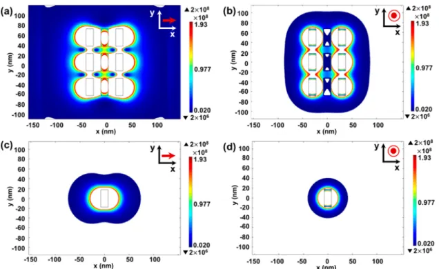
different orientations of the dipole.Figure 3shows the electric Figure 3. Electricfield intensity (E2) distribution at the NPL site: (a) for several NPLs when the dipoles are oriented in the
x axis and (b) in thez axis and (c) for a single NPL when the dipole is oriented in the x axis and (d) in the z axis.
Figure 4. Electricfield intensity (E2) distribution at the MoS
2layer for a 1 nm separation layer: (a) for several NPLs when the dipoles are
oriented in thex axis and (b) in the z axis and (c) for a single NPL when the dipole is oriented in the x axis and (d) in the z axis. ACS Nano
field intensity at the NPL site. As can be observed, E2 is
distributed along the layer of NPLs, which results from the delocalization of the dipoles. However, in the case of a single NPL, thefield is mainly localized around the NPL.
Figure 4shows the electricfield intensity in the MoS2layer
together with a 1 nm thick separation layer between the donor and the acceptor. It can be seen that the electricfield for an x dipole is more delocalized as compared to a dipole oriented in the z axis. We attribute this behavior to the screening effect resulting from the dipole orientation. Figure 5 shows the electricfield intensity distribution at the MoS2layer when the
dipole is oriented in the x and z axes using a 30 nm thick spacer. As can be observed from thisfigure, the electric field intensity is more distributed across the MoS2 in the case of
several NPLs as compared to the single NPL, where the electric field is more localized. Moreover, the electric field intensity is an order of magnitude larger for the x-oriented dipole than the z-oriented dipole, which emphasizes the anisotropic behavior of the CdSe-based NPL dipoles, as shown in the previous studies.47,48Thus, we can imply that the main contribution for the FRET rates comes from the x- and y-oriented dipoles. Therefore, the exciton delocalization along the NPLs and the electricfield intensity distributed along the MoS2acceptor layer support the FRET rate, leading to the 1/
d2decay.18,27,38−44
CONCLUSIONS
In conclusion, we have experimentally shown a Förster-type nonradiative energy transfer in the hybrid structure of CdSe/ CdS NPLs and MoS2monolayer thinfilm assembled together. We found near-unity FRET efficiency reaching 99.88% with an ultrafast FRET rate of 268.06 ns−1. Owing to the layer-to-layer dipole coupling between the CdSe/CdS donor and the MoS2 acceptor, the rate of FRET follows the d−2 scaling. This dependency is supported with a full numerical electromagnetic
model, which shows that the d−2 behavior comes from the delocalization of the electricfield distribution across the layers of NPLs and MoS2. In addition, the d−2dependency further
extends the Förster radius to a value of ∼33 nm, which is the longest reported to date, to the best of our knowledge. METHODS
Time-Resolved Fluorescence Spectroscopy. TRF spectrosco-py was carried out using a Pico Quant FluoTime 200 spectrometer. The NPLs were excited by a picosecond pulsed laser at a wavelength of 375 nm at low level intensity (≈10 nJ/cm2). Thus, the number of
photogenerated excitons was set much smaller than one photon per NPL on average (⟨N⟩ ≪ 1). The fluorescence decay curves were collected by a TimeHarp time-correlated single-photon counting unit. Then, we fitted the fluorescence decay curves to multiexponential decays through the FluoFit software by using the reconvolution mode of fitting to account for the instrument response function of the excitation pulse.
ASSOCIATED CONTENT
*
S Supporting InformationThe Supporting Information is available free of charge on the
ACS Publications websiteat DOI:10.1021/acsnano.8b04119.
Synthesis and characterization of 4-monolayer CdSe/ CdS core/crown nanoplateletes; growth of MoS2flakes
via chemical vapor deposition, sample characterization by atomic force microscopy; time-resolvedfluorescence decay curves from different positions of the samples along with their analyses; numerical fitting of FRET efficiency (PDF)
AUTHOR INFORMATION
Corresponding Author
*E-mail:[email protected].
ORCID
Hilmi Volkan Demir:0000-0003-1793-112X
Figure 5. Electricfield intensity (E2) distribution at the MoS
2layer for a 30 nm thick separation layer: (a) for several NPLs when the dipoles
are oriented in thex axis and (b) in the z axis and (c) for a single NPL when the dipole is oriented in the x axis and (d) in the z axis.
Notes
The authors declare no competingfinancial interest. ACKNOWLEDGMENTS
The authors gratefully acknowledge the financial support in part from Singapore National Research Foundation under the programs of NRF-NRFI2016-08 and the Science and Engineering Research Council, Agency for Science, Technol-ogy and Research (A*STAR) of Singapore, and in part from TUBITAK 114F326 and 115E679. H.V.D. also acknowledges support from TUBA. K.G. and O.E. acknowledge support from TUBITAK BIDEB.
REFERENCES
(1) Eda, G.; Maier, S. A. Two-Dimensional Crystals: Managing Light for Optoelectronics. ACS Nano 2013, 7, 5660−5665.
(2) Xia, F.; Wang, H.; Xiao, D.; Dubey, M.; Ramasubramaniam, A. Two-Dimensional Material Nanophotonics. Nat. Photonics 2014, 8, 899−907.
(3) Wang, Q. H.; Kalantar-Zadeh, K.; Kis, A.; Coleman, J. N.; Strano, M. S. Electronics and Optoelectronics of Two-Dimensional Transition Metal Dichalcogenides. Nat. Nanotechnol. 2012, 7, 699− 712.
(4) Ponraj, J. S.; Xu, Z.-Q.; Dhanabalan, S. C.; Mu, H.; Wang, Y.; Yuan, J.; Li, P.; Thakur, S.; Ashrafi, M.; Mccoubrey, K.; Zhang, Y.; Li, S.; Zhang, H.; Bao, Q. Photonics and Optoelectronics of Two-Dimensional Materials beyond Graphene. Nanotechnology 2016, 27, 462001.
(5) Bonaccorso, F.; Sun, Z.; Hasan, T.; Ferrari, A. C. Nat. Photonics 2010, 4, 611−622.
(6) Lee, J.; Dak, P.; Lee, Y.; Park, H.; Choi, W.; Alam, M. A.; Kim, S. Two-Dimensional Layered MoS2 Biosensors Enable Highly Sensitive Detection of Biomolecules. Sci. Rep. 2015, 4, 7352.
(7) Chen, Y.; Tan, C.; Zhang, H.; Wang, L. Two-Dimensional Graphene Analogues for Biomedical Applications. Chem. Soc. Rev. 2015, 44, 2681−2701.
(8) Song, Y.; Luo, Y.; Zhu, C.; Li, H.; Du, D.; Lin, Y. Recent Advances in Electrochemical Biosensors Based on Graphene Two-Dimensional Nanomaterials. Biosens. Bioelectron. 2016, 76, 195−212. (9) Ithurria, S.; Dubertret, B. Quasi 2D Colloidal CdSe Platelets with Thicknesses Controlled at the Atomic Level. J. Am. Chem. Soc. 2008, 130, 16504−16505.
(10) Ithurria, S.; Tessier, M. D.; Mahler, B.; Lobo, R. P. S. M.; Dubertret, B.; Efros, A. L. Colloidal Nanoplatelets with Two-Dimensional Electronic Structure. Nat. Mater. 2011, 10, 936−941.
(11) Olutas, M.; Guzelturk, B.; Kelestemur, Y.; Yeltik, A.; Delikanli, S.; Demir, H. V. Lateral Size-Dependent Spontaneous and Stimulated Emission Properties in Colloidal CdSe Nanoplatelets. ACS Nano 2015, 9, 5041−5050.
(12) Guzelturk, B.; Kelestemur, Y.; Olutas, M.; Delikanli, S.; Demir, H. V. Amplified Spontaneous Emission and Lasing in Colloidal Nanoplatelets. ACS Nano 2014, 8, 6599−6605.
(13) Kunneman, L. T.; Tessier, M. D.; Heuclin, H.; Dubertret, B.; Aulin, Y. V.; Grozema, F. C.; Schins, J. M.; Siebbeles, L. D. A. Bimolecular Auger Recombination of Electron-Hole Pairs in Two-Dimensional CdSe and CdSe/CdZnS Core/Shell Nanoplatelets. J. Phys. Chem. Lett. 2013, 4, 3574−3578.
(14) Tessier, M. D.; Javaux, C.; Maksimovic, I.; Loriette, V.; Dubertret, B. Spectroscopy of Single CdSe Nanoplatelets. ACS Nano 2012, 6, 6751−6758.
(15) Vitukhnovsky, A. G.; Lebedev, V. S.; Selyukov, A. S.; Vashchenko, A. A.; Vasiliev, R. B.; Sokolikova, M. S. Electro-luminescence from Colloidal Semiconductor CdSe Nanoplatelets in Hybrid Organic-Inorganic Light Emitting Diode. Chem. Phys. Lett. 2015, 619, 185−188.
(16) Prudnikau, A.; Chuvilin, A.; Artemyev, M. CdSe-CdS Nanoheteroplatelets with Efficient Photoexcitation of Central CdSe
Region through Epitaxially Grown CdS Wings. J. Am. Chem. Soc. 2013, 135, 14476−14479.
(17) Kramer, I. J.; Levina, L.; Debnath, R.; Zhitomirsky, D.; Sargent, E. H. Solar Cells Using Quantum Funnels. Nano Lett. 2011, 11, 3701−3706.
(18) Guzelturk, B.; Demir, H. V. Near-Field Energy Transfer Using Nanoemitters For Optoelectronics. Adv. Funct. Mater. 2016, 26, 8158−8177.
(19) Forster, T. Energiewanderung Und Fluoreszenz. Naturwissen-schaften 1946, 33, 166−175.
(20) Olutas, M.; Guzelturk, B.; Kelestemur, Y.; Gungor, K.; Demir, H. V. Highly Efficient Nonradiative Energy Transfer from Colloidal Semiconductor Quantum Dots to Wells for Sensitive Noncontact Temperature Probing. Adv. Funct. Mater. 2016, 26, 2891−2899.
(21) Rowland, C. E.; Fedin, I.; Zhang, H.; Gray, S. K.; Govorov, A. O.; Talapin, D. V.; Schaller, R. D. Picosecond Energy Transfer and Multiexciton Transfer Outpaces Auger Recombination in Binary CdSe Nanoplatelet Solids. Nat. Mater. 2015, 14, 484−489.
(22) Guzelturk, B.; Olutas, M.; Delikanli, S.; Kelestemur, Y.; Erdem, O.; Demir, H. V. Nonradiative Energy Transfer in Colloidal CdSe Nanoplatelet Films. Nanoscale 2015, 7, 2545−2551.
(23) Chen, Z.; Berciaud, S.; Nuckolls, C.; Heinz, T. F.; Brus, L. E. Energy Transfer from Individual Semiconductor Nanocrystals to Graphene. ACS Nano 2010, 4, 2964−2968.
(24) Gaudreau, L.; Tielrooij, K. J.; Prawiroatmodjo, G. E. D. K.; Osmond, J.; De Abajo, F. J. G.; Koppens, F. H. L. Universal Distance-Scaling of Nonradiative Energy Transfer to Graphene. Nano Lett. 2013, 13, 2030−2035.
(25) Lightcap, I. V.; Kamat, P. V. Fortification of CdSe Quantum Dots with Graphene Oxide. Excited State Interactions and Light Energy Conversion. J. Am. Chem. Soc. 2012, 134, 7109−7116.
(26) Yeltik, A.; Kucukayan-Dogu, G.; Guzelturk, B.; Fardindoost, S.; Kelestemur, Y.; Demir, H. V. Evidence for Nonradiative Energy Transfer in Graphene-Oxide-Based Hybrid Structures. J. Phys. Chem. C 2013, 117, 25298−25304.
(27) Shafran, E.; Mangum, B. D.; Gerton, J. M. Energy Transfer from an Individual Quantum Dot to a Carbon Nanotube. Nano Lett. 2010, 10, 4049−4054.
(28) Prins, F.; Goodman, A. J.; Tisdale, W. A. Reduced Dielectric Screening and Enhanced Energy Transfer in Single- and Few-Layer MoS2. Nano Lett. 2014, 14, 6087−6091.
(29) Raja, A.; Montoya-Castillo, A.; Zultak, J.; Zhang, X. X.; Ye, Z.; Roquelet, C.; Chenet, D. A.; Van Der Zande, A. M.; Huang, P.; Jockusch, S.; Hone, J.; Reichman, D. R.; Brus, L. E.; Heinz, T. F. Energy Transfer from Quantum Dots to Graphene and MoS2: The
Role of Absorption and Screening in Two-Dimensional Materials. Nano Lett. 2016, 16, 2328−2333.
(30) Goodfellow, K. M.; Chakraborty, C.; Sowers, K.; Waduge, P.; Wanunu, M.; Krauss, T.; Driscoll, K.; Vamivakas, A. N. Dimensional Semiconductor Distance-Dependent Energy Transfer between CdSe/ CdS Quantum Dots and a Two-Dimensional Semiconductor. Appl. Phys. Lett. 2016, 021101, 1−5.
(31) Federspiel, F.; Froehlicher, G.; Nasilowski, M.; Pedetti, S.; Mahmood, A.; Doudin, B.; Park, S.; Lee, J. O.; Halley, D.; Dubertret, B.; Gilliot, P.; Berciaud, S. Distance Dependence of the Energy Transfer Rate from a Single Semiconductor Nanostructure to Graphene. Nano Lett. 2015, 15, 1252−1258.
(32) Abécassis, B.; Tessier, M. D.; Davidson, P.; Dubertret, B. Self-Assembly of CdSe Nanoplatelets into Giant Micrometer-Scale Needles Emitting Polarized Light. Nano Lett. 2014, 14, 710−715.
(33) Kelestemur, Y.; Dede, D.; Gungor, K.; Usanmaz, C. F.; Erdem, O.; Demir, H. V. Alloyed Heterostructures of CdSexS1−x
Nano-platelets with Highly Tunable Optical Gain Performance. Chem. Mater. 2017, 29, 4857−4865.
(34) Lee, C.; Yan, H.; Brus, L.; Heinz, T.; Hone, J.; Ryu, S. Anomalous Lattice Vibrations of Single-and Few-Layer MoS2. ACS
Nano 2010, 4, 2695−2700. ACS Nano
(35) Li, H.; Zhang, Q.; Yap, C. C. R.; Tay, B. K.; Edwin, T. H. T.; Olivier, A.; Baillargeat, D. From Bulk to Monolayer MoS2: Evolution
of Raman Scattering. Adv. Funct. Mater. 2012, 22, 1385−1390. (36) Mak, K. F.; Lee, C.; Hone, J.; Shan, J.; Heinz, T. F. Atomically Thin MoS2: A New Direct-Gap Semiconductor. Phys. Rev. Lett. 2010,
136805, 2−5.
(37) Peng, X.; Misewich, J. A.; Wong, S. S.; Sfeir, M. Y. Efficient Charge Separation in Multidimensional Nanohybrids. Nano Lett. 2011, 11, 4562−4568.
(38) Chanyawadee, S.; Lagoudakis, P. G.; Harley, R. T.; Charlton, M. D. B.; Talapin, D. V.; Huang, H. W.; Lin, C. H. Increased Color-Conversion Efficiency in Hybrid Light-Emitting Diodes Utilizing Non-Radiative Energy Transfer. Adv. Mater. 2010, 22, 602−606.
(39) Rindermann, J. J.; Pozina, G.; Monemar, B.; Hultman, L.; Amano, H.; Lagoudakis, P. G. Dependence of Resonance Energy Transfer on Exciton Dimensionality. Phys. Rev. Lett. 2011, 107, 1−5. (40) Lin, T. N.; Huang, L. T.; Shu, G. W.; Yuan, C. T.; Shen, J. L.; Lin, C. a J.; Chang, W. H.; Chiu, C. H.; Lin, D. W.; Lin, C. C.; Kuo, H. C. Distance Dependence of Energy Transfer from InGaN Quantum Wells to Graphene Oxide. Opt. Lett. 2013, 38, 2897−2899. (41) Agranovich, V. M.; Rupasov, V. I.; Silvestri, L. Hybrid Resonant Organic-Inorganic Nanostructures for Novel Light Emitting Devices and Solar Cells. Phys. Status Solidi C 2010, 7, 1684−1687.
(42) Becker, K.; Lupton, J. M.; Müller, J.; Rogach, A. L.; Talapin, D. V.; Weller, H.; Feldmann, J. Electrical Control of Förster Energy Transfer. Nat. Mater. 2006, 5, 777−781.
(43) Kuhn, H. Classical Aspects of Energy Transfer in Molecular Systems. J. Chem. Phys. 1970, 53, 101−108.
(44) Yu, Y.-J.; Kim, K. S.; Nam, J.; Kwon, S. R.; Byun, H.; Lee, K.; Ryou, J.-H.; Dupuis, R. D.; Kim, J.; Ahn, G.; Ryu, S.; Ryu, M.-Y.; Kim, J. S. Temperature-Dependent Resonance Energy Transfer from Semiconductor Quantum Wells to Graphene. Nano Lett. 2015, 15, 896−902.
(45) Govorov, A. O.; Carmeli, I. Hybrid Structures Composed of Photosynthetic System and Metal Nanoparticles: Plasmon Enhance-ment Effect. Nano Lett. 2007, 7, 620−625.
(46) Hernández-Martínez, P. L.; Govorov, A. O. Exciton Energy Transfer between Nanoparticles and Nanowires. Phys. Rev. B: Condens. Matter Mater. Phys. 2008, 78, 1−7.
(47) Scott, R.; Heckmann, J.; Prudnikau, A. V.; Antanovich, A.; Mikhailov, A.; Owschimikow, N.; Artemyev, M.; Climente, J. I.; Woggon, U.; Grosse, N. B.; Achtstein, A. W. Directed Emission of CdSe Nanoplatelets Originating from Strongly Anisotropic 2D Electronic Structure. Nat. Nanotechnol. 2017, 12, 1155−1160.
(48) Gao, Y.; Weidman, M. C.; Tisdale, W. A. CdSe Nanoplatelet Films with Controlled Orientation of Their Transition Dipole Moment. Nano Lett. 2017, 17, 3837−3843.