Materials Research Express
PAPER
Growth and characterization of nanocrystalline
SrTiO
x
films: room temperature deposition using
RF sputtering system in a pure argon environment
To cite this article: T Bayrak and E Goldenberg 2017 Mater. Res. Express 4 055016View the article online for updates and enhancements.
Related content
Optical characterization of filtered vacuum arc deposited zinc oxide thin films
E Çetinörgü, S Goldsmith, V N Zhitomirsky et al.
-Structural, optical and microwave dielectric studies of Co doped MgTiO3 thin films fabricated by RF magnetron sputtering
T Santhosh Kumar, Pallabi Gogoi, S Bhasaiah et al.
-Effect of the amorphous-to-crystalline transition in Ba0.5Sr0.5TiO3 thin films on optical and microwave dielectric properties
K Venkata Saravanan, K Sudheendran, M Ghanashyam Krishna et al.
-Recent citations
The effect of rare earth ions on structural, morphological and thermoelectric properties of nanostructured tin oxide based perovskite materials
P Rajasekaran et al
-© 2017 IOP Publishing Ltd
1. Introduction
Perovskite SrTiO3 (STO) is a promising oxide material due to its high charge store capacity, chemically stable
structure, low leakage current, high dielectric constant and transparency, smooth surface and small lattice mismatch with other perovskite oxides [1, 2]. It has a large direct band gap of ~3.2 eV, and thin films of STO show paraelectric and ferroelectric properties [3, 4]. Thus, STO can be used in a wide range of applications, including microcapacitors, optical switches, electro-optic devices, dynamic random access memories (DRAM) and metal-insulator-metal (MIM) resistive switchers [5–8]. For next generation DRAM and high-density MIM structures oxide thickness below 0.5 nm and low leakage current are particularly important [9]. Another appealing feature of STO is the tuneable phase shifters for microwave circuits. STO has a field dependent dielectric constant, which allows the development of tuneable devices [10]. Lately it was shown that amorphous STO has a bipolar switching mechanism with a high switching ratio due to the oxygen vacancies and point defects in its microstructure [11–13]. In recent years, thin films of STO have been grown by a variety of deposition processes at high temperatures, including pulse laser deposition, atomic layer deposition, molecular beam epitaxy, RF sputtering, sol-gel and laser ablation [14–23]. Films grown at high temperatures have a high film packing density and high dielectric values. Improved film properties and device performances are needed for low temperature grown films. In the literature, reported dielectric constants of STO films vary from 12 to >950 for different film thicknesses ranging from 10 nm to 1000 nm and different deposition processes, from RT to 800 °C [14–24]. The correlation between the growth parameters such as substrate and annealing temperatures and film microstructure, optical or electrical properties of crystalline STO thin films have already been described in the literature [14, 23–25]. However, the results appear
T Bayrak and E Goldenberg
055016
MRX
© 2017 IOP Publishing Ltd 4
Mater. Res. Express
MRX 2053-1591 10.1088/2053-1591/aa6df3 5
1
7
Materials Research Express
16
May
2017
Growth and characterization of nanocrystalline SrTiO
x
films: room
temperature deposition using RF sputtering system in a pure argon
environment
T Bayrak1,2 and E Goldenberg3
1 Institute of Materials Science and Nanotechnology, Bilkent University, Ankara 06800, Turkey 2 National Nanotechnology Research Center (UNAM), Bilkent University, 06800 Ankara, Turkey 3 Department of Physics, Advanced Research Laboratories, Bilkent University, 06800 Ankara, Turkey
E-mail: [email protected] and [email protected]
Keywords: strontium titanate, annealing, nanocrystalline thin films, ferroelectrics, RF sputtering
Abstract
We report a comprehensive description of the structure, optical and electrical properties of as-deposited and annealed SrTiOx (STO) thin films. Nanocrystalline STO films were deposited
on p-type Si (1 0 0) and UV-grade fused silica substrates by RF magnetron sputtering at room temperature in a pure argon environment. Well adhered and transparent films with very smooth surfaces were obtained. As-deposited films showed 70% transparency in the visible spectrum, transparency increased to 77% after annealing at 700 °C. The direct and indirect optical band gaps were found to be 2.88 eV and 2.44 eV, for as-deposited films. For annealed films, indirect band gap increased to 2.57 eV while the direct optical band gap value remained constant. Upon annealing, the refractive indices (n) of the films decreased from 2.36 to 2.32. Ag/STO/p-Si device structures were also fabricated and characterized by current–voltage, capacitance-voltage and dielectric measurements. The calculated values are compared with experimental data from the literature and discussed in terms of device performances. A butterfly loop-type hysteresis curve was observed for the voltage-dependent capacitance measurement in annealed thin film devices. Dielectric constants were calculated as 31.7 and 57.4 for as-deposited and annealed films at 100 kHz, respectively. Charge storage capacity was found to be >4.5 µC cm−2 for as-deposited and 3.5 µC cm−2 for annealed films. PAPER 2017 RECEIVED 15 March 2017 REVISED 11 April 2017 ACCEPTED FOR PUBLICATION 19 April 2017 PUBLISHED 16 May 2017
https://doi.org/10.1088/2053-1591/aa6df3
T Bayrak and E Goldenberg
rather inconsistent since the microstructure is very sensitive to the deposition method as well as post-deposition annealing. In addition, despite the widespread use of these films, there are no corresponding data in the literature on the effects of pure Ar environment and low temperature growth on the physical characteristics of STO films deposited by sputtering.
In the present paper, the effect of Ar and low temperature growth on the physical characteristics of STO films deposited using RF magnetron sputtering was systematically investigated and the calculated values are compared with experimental data from the literature.
2. Experimental procedure
2.1. Film deposition
All SrTiOx (STO) thin films were deposited at room temperature (RT) on Si and UVFS substrates using an off-plane axis RF-magnetron sputtering system in a pure Ar environment. Radio frequency (RF) plasma power of 75 W and constant pressure of 0.67 Pa were used as constant deposition parameters. Film thickness was ~125 nm which was confirmed by ellipometer analysis. Prior to deposition the base pressure of the chamber was <6.5 × 10⁻⁶
Torr (0.9 mPa). Stoichiometric SrTiO3 ceramic target (50 mm, purity 99.9%) with a smooth surface was used as
cathode material. Si and UV-fused silica (UVFS) substrates were cleaned in isopropanol and later rinsed in DI water. As-deposited films were annealed at 700 °C for an hour in O2 ambient (200 sccm) using an ATV-Unitherm
(RTA SRO-704) rapid thermal annealing system. The heating rate was ~10 °C s−1, and samples were removed from the annealing chamber after the system was cooled down to below 50 °C. The details of the deposition parameters are given in table 1.
2.2. Film characterization
The microstructure of films was evaluated with grazing incidence x-ray diffraction (GIXRD) measurements using Cu-Kα (1.5406 Å) radiation with an incident angle of 0.3° and diffraction angles between 20° and 80°. Bulk film chemical composition was evaluated by x-ray photoelectron spectroscopy (XPS) equipped with a monochromatized Al Kα x-ray source (1486.6 eV). An Ar ion beam with an acceleration voltage of 1 kV was used
to etch samples for ~30 s. The data revealed the presence of Sr, Ti, O and Ar elements in the films.
Surface morphologies of the deposited films were investigated using scanning electron (SEM, FEI Nova NanoSEM 430) and atomic force microscopes (AFM, Asylum Research MFP-3D), the latter operating in tapping mode. Optical characterization was performed using variable angle spectroscopic ellipsometry (VASE, J A Wool-lam Co.) and spectrophotometry (Ocean Optics HR4000CG-UV-NIR). All samples were measured at RT for wavelengths, λ, ranging from 250 to 1000 nm. The optical constants were modelled using the Lorentz dispersion
formula for n(λ) and k(λ), and a four-layer model including substrate, film, surface roughness and ambient. All n and k values correspond to values recorded at a wavelength of 550 nm. Absorption coefficients were calculated
from k(λ) values (α(λ) = 4πk(λ)/λ). The optical band gap energy (Eg) was evaluated using Tauc formula [25].
The direct and indirect band gaps were determined from (αhv)2 and (αhv)1/2 versus hv, plots, respectively.
Ag/STO/p-Si (1 0 0) structures have been fabricated on p-Si substrates to determine the dielectric properties of as-deposited and annealed STO thin films. Frequency-dependent dielectric properties of the fabricated test structures were measured using an Agilent E4980A Precision LCR meter in a frequency range of 200 Hz to 1 MHz under zero bias at RT. Dielectric constants of the films were calculated using the parallel plate capacitance model (C = ε0 × εr × A/t, where C, t, ε0, εr, and A are the accumulation capacitance, film thickness, permittivity of free
space, dielectric constant of the film, and area of the electrodes, respectively). Frequency-dependent dielectric loss functions of the as-deposited and annealed films were calculated using the formula tanδ = G/ωC, where G
is conductivity (as determined by LCR measurements), ω is 2πf and C is the accumulation capacitance. In
addi-tion to frequency dependent capacitance measurements, thin film current–voltage (I–V) characteristics of the test structures were also measured using a semiconductor parameter analyzer (Keithley 4200-SCS) connected to a DC probe station (Cascade Microtech PM-5) for the determination of the breakdown field (E = V /d, d
Table 1. Deposition parameters for nanocrystalline STO thin films.
Deposition parameters
Base pressure (mPa) <0.90
Deposition pressure (Pa) 0.67
RF power (W) 75
Total gas flow (sccm) 30
Target size (mm) 50
Target-substrate distance (mm) 50
Deposition time (min) 10
is the film thickness) and the leakage current. The charge storage capacity (CSC), was calculated from the equa-tion CSC = ε0 × εr × Ebd.
3. Results and discussion
3.1. Film microstructure, composition and surface morphology
STO films were deposited in a pure Ar environment with a plasma power of 75 W. It is well known that the formation of the crystalline phases of SrTiO3 depends on growth parameters (such as substrate temperature,
pressure, and Ar flow) and post-deposition annealing. In the present work, all as-deposited films were amorphous phase, and they retain their amorphous structure with some increased nanocrystallinity after annealing at 700 °C. XPS survey scans were performed for as-deposited and annealed films to determine the elemental composi-tions of the STO films after 30 s in situ Ar etching. The Sr/Ti elemental ratio (stoichiometry) was found to be 0.74, while the oxygen concentration of as-deposited films was 75.34 at.%. Physical entrapment or chemical bonding of additional oxygen anions might be the reason for the observed excess oxygen [18]. Wang et al noted that water remaining in the vacuum chamber may react with oxygen to form hydroxyl groups, and a similar process may have been responsible for the excess oxygen content in our STO films [15]. Furthermore, after the films were etched in
situ with a beam of Ar ions 2.4% Ar was detected in the film bulk independent of annealing conditions. It is likely
that the Ar inclusion results from the Ar etching process used during the XPS measurements [19], since no Ar was found on film surface.
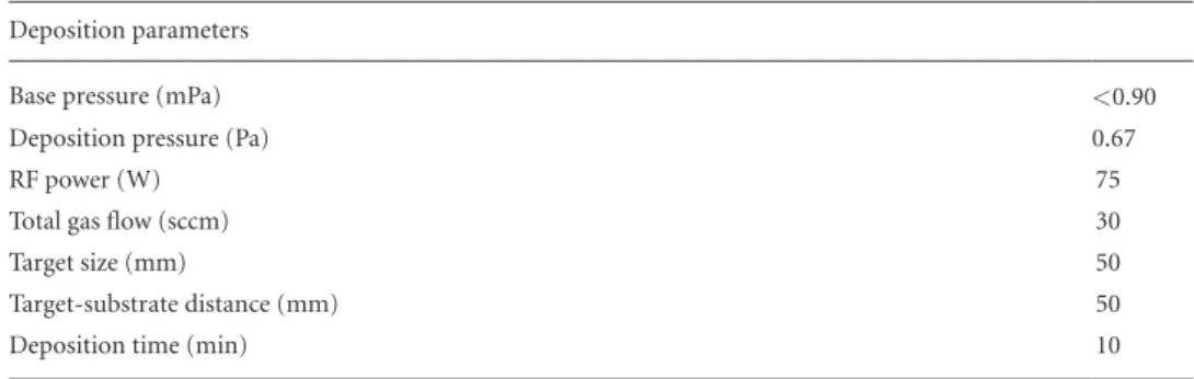
Surface morphologies of all as-deposited and annealed films were evaluated by SEM and AFM analyses. As-deposited films showed very smooth surfaces. In figure 1, an SEM image of annealed STO thin film surface is presented as an example. After 1 h annealing, at 700 °C, the grain size was increased and flakes had approved. This result indicates that annealing increases the local density of the film, resulting flake-like formations.
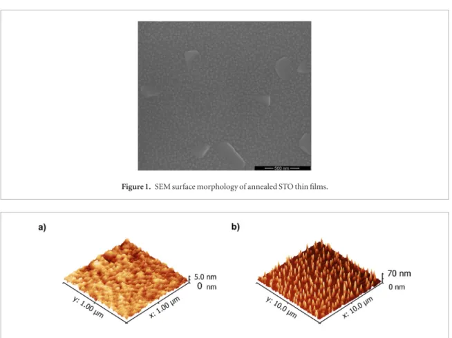
Figures 2(a) and (b) show the 3D AFM scans of the as-deposited and annealed STO thin films. As-deposited STO films showed relatively smooth surface with a root-mean-square roughness (rms) of 0.23 nm, whereas, as can be seen from figure 2(b) the cluster-like nano-grains were distributed uniformly with a rms value of 8.3 nm, which is in good agreement with SEM images and optical analyses. An increase of surface roughness after the annealing process might be explained by the formation of the cluster like nano-grains. Furthermore, nanocrystal grain boundaries might be responsible from the formation of grain-boundary grooves, which significantly contributes to a rougher film surface [25–27]. As mentioned in our previous study, rms roughness in STO films deposited at 0.40 Pa with 0% O2 flow rate is lower than 0.2 nm [28]. We observe that increase in surface roughness under high deposition pressure.
This can be explained by the increased deposition rate in this pressure range in RF sputtering [29]. Figure 1. SEM surface morphology of annealed STO thin films.
T Bayrak and E Goldenberg
3.2. Optical properties
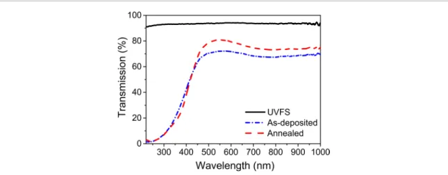
Effect of deposition parameters on the optical properties of the films were studied by spectrophotometry and spectroscopic ellipsometry. Figure 3 shows the optical transmission of as-deposited and annealed STO films and that of the substrate. As-deposited films were transparent (70%), and annealing at 700 °C improved their optical transmission (77%). In addition, a significant decrease in the UV transmission was observed at wavelengths below 450 nm, which is caused by the main band gap absorption for both as-deposited and annealed films. The absorption edge steepness increased upon annealing. Increase in optical transmission and steepness in absorption edge might be attributed to decreased light scattering loss after annealing and improved film microstructure. The widening of the absorption edge, particularly observed for this thin film, maybe due to strain-induced defects and the amorphous phase. Gupta et al also ascribed the observed absorption edge increase to the grain size increase with annealing, in contrast to stress or void formations [30].
In figures 4(a) and (b) the refractive index and extinction coefficients, obtained from ellipsometry analyses of films are plotted. Film refractive index has maxima 2.52 and 2.58 at 400 nm and decreases to 2.20 and 2.15 at 1200 nm for as-deposited and annealed films respectively, obeying normal dispersion in optics. The dispersion curves show a similar behaviour for both as-deposited and annealed STO films as a function of wavelength (figures 4(a) and (b)). Near the absorption edge (~380–400 nm), which is also presented in figure 3, the refractive index has a well-defined maxima for both films. However, the maxima are slightly shifted to longer wavelengths after annealing, indicating change in the optical band edge as confirmed by band gap calculations [31]. Furthermore, in the VIS range, the refractive indices of nanocrystalline STO films are found to be 2.36 and 2.31 (@550 nm) for as-deposited and annealed films, respectively. Its value decreased with annealing, however, the observed values is larger than the reported amorphous (1.83–2.06) and polycrystalline (2.05–2.12) films [28, 32–34]. It should be noted that the film thickness which is generally lower than 100 nm has affects film properties, however, according to our best knowledge there is no comparative information on the effect of film thickness on thin STO films. The optical absorption (>450 nm) of the as-deposited films, and of those annealed was low, resulting in an extinction coefficient of k ~ 10−2–10−3. The absorption value was also found to decrease slightly after annealing, can be attrib-uted to grain growth and while decrease in grain boundary scattering as supported both the XRD measurements and by the optical transmission of the coatings. Furthermore, as can be seen from figure 4(b), the sharpness of the extinction coefficient is increased. This might be due to improved film microstructure and also lower film stress
Figure 3. Spectral optical transmission plots of as-deposited and annealed STO thin films and UVFS substrate as reference.
Annealing was performed at 700 °C for 1 h in O2 environment.
Figure 4. Refractive index and extinction coefficient plots of (a) as-deposited and (b) annealed STO thin films. Mater. Res. Express 4 (2017) 055016
upon annealing. It is known that, in polycrystalline thin films, imperfections, such as the presence of mechanical stress due to lattice distortion in the grain-boundary regions can influence the electronic structure and, hence, the below-band-edge optical absorption [35]. Although the optical constants might also depend on film stoichiometry we did not observe the this effect in our work. Similar to our results, Gupta et al observed refractive index increasing with annealing temperature up to 400 °C, while annealing above 400 °C decreased it to the bulk value. They also noted that the presence of the crack formations after the annealing process might be responsible for the decrease of the refractive index [30]. We did not observe such dependence.
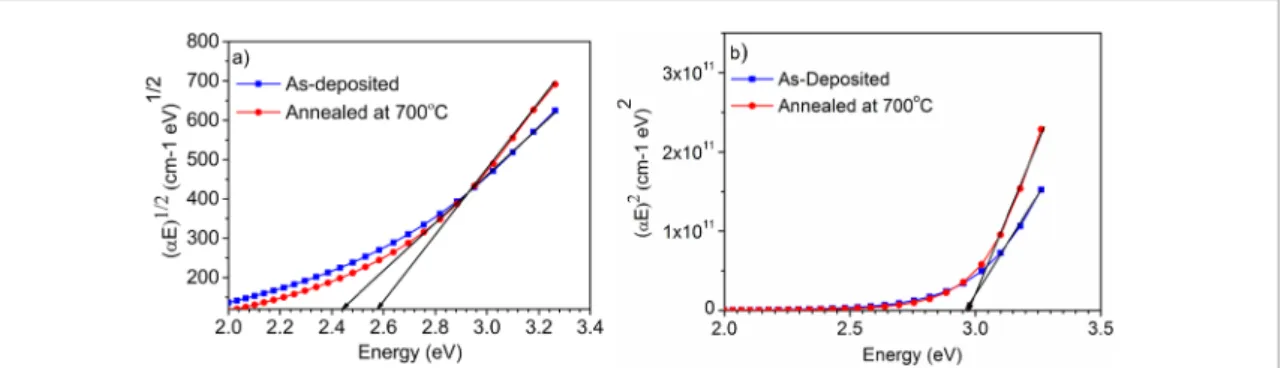
The optical band gaps of the films are calculated using the data obtained from ellipsometry analyses. The direct (indirect) band gap energies of the as-deposited and annealed films are found to be 2.44 (2.88) eV, and 2.57 (2.88) eV in figure 5(a) and 5(b), respectively. Direct and indirect band gap values are lower than the noted values in our previ-ous study for 0.40 Pa deposition pressure [28]. The reduction in band gap energies might be due to the variation in the oxidation state of the film and stoichiometric changes with increasing deposition pressure up to 0.67 Pa. Indirect optical band gap energy values were lower than direct band gap energies. Benthem et al [36] reported similar results on the variation of optical band gaps of Fe-doped STO thin films, and stated that STO films have well determined indirect (3.25 eV) and direct (3.75 eV) band gap energies. SrTiO3 bulk films have 3.2 eV optical band gap. Moreover,
Frye et al [37] studied the effect reducing the oxidation state single crystalline STO films using ellipsometry and hall measurements, and found decreasing on optical band gap. Kok et al also studied temperature dependence of optical absorption edge and near infrared absorption of bulk crystalline SrTiO3. They noted, that the optical absorption is
3.25 ± 0.03 eV for 4 K and decreases to 1.2 ± 0.1 eV at the melting temperature of SrTiO3 (2350 K) [38].
In the present study, indirect band gap energies of films deposited in pure Ar environment are found to be lower compared to the data already reported in literature. However, following the annealing process, the observed indirect band gap energy values increased, this might be due to increased oxidation. The observed changes in opti-cal constants of the films are in agreement with the literature.
3.3. Electrical properties
Film electrical breakdown voltage, dielectric constants, and tan loss values were extracted from current–voltage and frequency dependent capacitance-voltage measurements. In figure 6, current density of the annealed STO thin film is presented as a function of the applied voltage. The annealed film showed a breakdown at −8.8 V. However, no breakdown was observed in the range of −20 to +20 V for as-deposited film. The leakage current was found to be relatively small (<10−6 A cm−2 at bias of ±0 V).
Figure 5. Energy band gap values of as-deposited and annealed films corresponding to (a) indirect and (b) direct band gaps.
T Bayrak and E Goldenberg
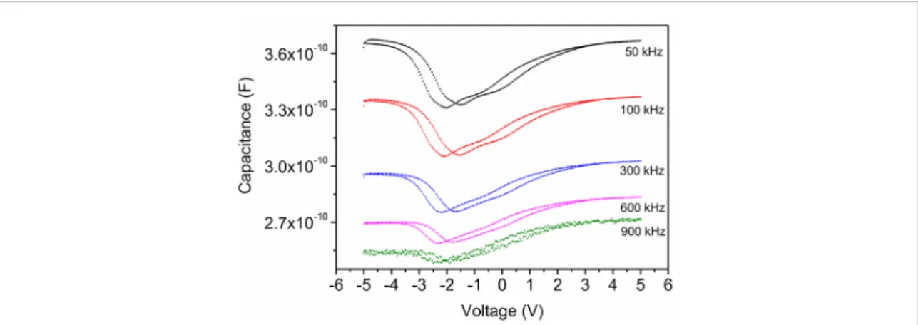
Frequency dependent capacitance of the Ag/STO/p-Si structures were acquired at five different frequencies (50–100–300–600 and 900 kHz) for both as-deposited and annealed films. As-deposited films showed two distinct regimes of accumulation/inversion. The annealed films exhibited hysteresis behaviour independent of the meas-urement frequency. Figure 7 shows the dc voltage sweeping from positive to negative bias at 50, 100, 300, 600 and 900 kHz, and the following reverse sweeping for annealed films.
As can be seen from the plots, a butterfly-loop hysteresis was observed. However, as-deposited films did not show similar behaviour. Dawber et al classified this behaviour as one of the defining characteristics of ferroelec-tric materials. They indicated that the effect might be the result of the switching mechanism of the ferroelecferroelec-tric domains in nanocrystal regions [39]. Other reports in the literature attribute this behaviour to the charge injection, carrier trapping and/or space charge redistribution in the under electrode area, or net positive charges creating a positive shift during the voltage sweep [21, 39]. In our work, the cause for this difference is unknown and fur-ther investigations, such as electric field dependent polarity or pulsed C-V measurements, are required to better understand this phenomenon.
It is well known that all capacitive responses are due to the insulator when the MIS device is biased on accu-mulation. As-deposited film exhibits accumulation at 0 V bias; consequently, frequency dependent capacitance measurements were taken at 0 V bias for all films and assumed to represent the behaviour of the insulating STO layer. Frequency dependent dielectric constant and dielectric loss values of both films are given in figure 8.
The dielectric constant (εr) decreased with increasing frequency for annealed films, while as-deposited films showed a stable dielectric constant value with increasing frequency. Dielectric losses are found to increase with fre-quency in both annealed and as-deposited films. εr values decreased with increasing frequency for annealed films, while as-deposited films showed a stable dielectric constant value with increasing frequency. Dielectric losses, in contrast, are found to increase with frequency in both annealed and as-deposited films. According to literature nanocrystalline thin film materials show similar frequency dispersion for the dielectric constants [18, 40, 41]. It is mostly attributed to a combination of relaxation phenomena inside the film bulk and charging–de-charging mechanisms both in the bulk and at the interface [14].
Dielectric constants of the films at 100 kHz were determined to be 31.7 and 57.4 for as-deposited and annealed films, respectively. Dielectric losses were found to be 0.03 for as-deposited and 0.31 for annealed films at the same frequency. The observed low dielectric values might be attributed to the small crystallite size formation due to low temperature growth and low film thickness (<200 nm). Ebd and the corresponding CSC values were calculated
Figure 7. C-V characterization of the annealed STO thin film with different frequencies (50, 100, 300, 600, 900 kHz).
Figure 8. Dielectric constants and dielectric losses of as-deposited and annealed STO thin film as a function of frequency. Mater. Res. Express 4 (2017) 055016
for both as-deposited and annealed films and found to be >1.6 MV cm−1 and >4.5 µC cm−2 for as-deposited and
0.69 MV cm−1 and 3.5 µC cm−2 for annealed films, respectively.
4. Conclusions
We demonstrated the effects of pure argon environment deposition at RT and annealing process on STO thin film properties prepared by RF magnetron sputtering. Nanocrytalline films were obtained independent of the deposition parameters and the post-deposition annealing conditions. All films exhibited relatively good transparency with good adhesion. The electrical characteristics of MIS device structures showed that dielectric constant and dielectric loss values are affected by the measurement frequency and annealing. Relatively high dielectric constant, low loss with high charge storage capacity and the interesting switching mechanism suggested that low temperature grown SrTiOx thin films are promising for DRAM applications.
Acknowledgments
This work was performed at UNAM—Institute of Materials Science and Nanotechnology. Authors acknowledge the Scientific and Technological Research Council of Turkey (TUBITAK) (Project #115F077) for their financial support and Mr A Haider for his assistance in SEM measurements.
References
[1] Kanemitsu Y and Yamada Y 2011 Phys. Status Solidi B 248416–21
[2] Lee J H, Cho Y J, Min Y S, Kim D and Rhee S W 2002 J. Vac. Sci. Technol. 201828–30
[3] Pontes F M, Lee E J H, Leite E R, Longo E and Varela J A 2000 J. Mater. Sci. Mater. 354783–7
[4] Wordenweber R, Hollmann E, Ali M, Schubert J, Pickartz G and Lee T K 2007 J. Eur. Ceram. Soc. 272899
[5] Schroeder H, Pandian R and Miao J 2011 Phys. Status Solidi A 208300–16
[6] Grundmann M, Frenzel H, Lajn A, Lorenz M, Schein F and von Wenckstern H 2010 Phys. Status Solidi A 2071437–49
[7] Zhu Y, Li M, Zhou H, Hu Z, Liu X, Fang X, Sebo B, Fang G and Zhao X 2012 J. Phys. D: Appl. Phys. 45375303
[8] Yang M, Bao D H and Li S W 2013 J. Phys. D: Appl. Phys. 46495111
[9] He G and Sun Z 2012 High-k Gate Dielectrics for CMOS Technology (New York: Wiley) p 45 [10] Fuchs D, Schneider C W, Schneider R and Rietschel H 1999 J. Appl. Phys. 857362–9
[11] Nili H, Walia S, Balendhran S, Strukov D B, Bhaskaran M and Sriram S 2014 Adv. Funct. Mater. 246741–50
[12] Nili H et al 2015 Adv. Funct. Mater. 253172–82
[13] Szot K, Dittmann R, Speier W and Waser R 2007 Phys. Status Solidi 186–8
[14] Wang Z, Kugler V, Helmersson U, Evangelou E K, Konofaos N, Nakao S and Jin P 2002 Phil. Mag. B 82891–903
[15] Ang C, Yu Z, Cross L E, Guo R and Bhalla A S 2001 Appl. Phys. Lett. 79818–20
[16] Pontes F M, Lee E J, Leite E R, Longo E and Varela J A 2000 Adv. Mater. Res. 35 4783–7 [17] Hofman W, Hofman S and Waser R 1997 Thin Solid Films 30566
[18] Joshi P C and Krupanidhi S B 1993 J. Appl. Phys. 737627
[19] Kamalasanan M N, Kumar N D and Chandra S 1993 J. Appl. Phys. 7467
[20] Raq G M and Krupanidhi S B 1994 J. Appl. Phys. 752604
[21] Liu C Y and Tseung-Yuen T 2004 J. Eur. Ceram. Soc. 241449–53
[22] Eisenbeiser K et al 2000 Appl. Phys. Lett. 761324
[23] Popovici M, Kaczer B, AfanasV V, Sereni G, Larcher L, Redolfi A and Elshocht S V 2016 Phys. Status Solidi 10420–5
[24] Choudhury B K, Rao K V and Choudhury R N P 1989 J. Mater. Sci. Mater. 243469–74
[25] Panomsuwan G, Osamu T and Nagahiro S 2013 Phys. Status Solidi A 210311–9
[26] Campet G, Geoffroy C, Manaud J P, Portier J, Sun Z W, Salardenne J and Keou P 1991 Mater. Sci. Eng. B 845–52
[27] Akhavan O and Azimirad R 2009 J. Phys. D: Appl. Phys. 42065404
[28] Goldenberg E, Bayrak T, Ozgit-Akgun C, Haider A, Leghari S A, Kumar M and Biyikli N 2015 Thin Solid Films 5903–9
[29] Priestland C R and Hersee S D 1972 Vacuum 22103–6
[30] Gupta V and Abhai M 1996 J. Appl. Phys. 801063–73
[31] Cetinorgu E, Goldsmith S, Zhitomirsky V N, Boxman R L and Bungay C L 2006 Semicond. Sci. Technol. 211303
[32] Longo V, Leick N, Roozeboom F and Kessels W M 2013 ECS J. Solid State Sci. Technol. 215–22
[33] Zollner S et al 2000 J. Vac. Sci. Technol. B 1842–54
[34] Bayrak T, Kizir S, Kahveci E, Bıyıklı N and Goldenberg E 2017 J. Vac. Sci. Technol. 35021505
[35] Dietrich A, Schmalzbauer K, Hoffmann H and Szczyrbowski J 1984 Thin Solid Films 12219–29
[36] van Benthem K, Elssser C and French R H 2001 J. Appl. Phys. 9012
[37] Frye A, French R H and Bonnell D A 2003 Z. Metall. 94226–32
[38] Kok D J, Irmscher K, Naumann M, Guguschev C, Galazka Z and Uecker R 2015 Phys. Status Solidi A 2121880–7
[39] Dawber M, Rabe K M and Scott J F 2005 Rev. Mod. Phys. 771083
[40] Hahn Y B and Kim D O 1999 J. Vac. Sci. Technol. A 171982