INVESTIGATION OF OPTICAL RESIDUAL
ABSORPTION IN GRAPHENE
A THESIS SUBMITTED TO
THE GRADUATE SCHOOL OF ENGINEERING AND SCIENCE OF BILKENT UNIVERSITY
IN PARTIAL FULFILMENT OF THE REQUIREMENTS FOR THE DEGREE OF MASTER OF SCIENCE IN PHYSICS
By
Zeinab Eftekhari
February 2018
ii
INVESTIGATION OF OPTICAL RESIDUAL ABSORPTION IN GRAPHENE By Zeinab Eftekhari
February 2018
We certify that we have read this thesis and that in our opinion it is fully adequate, in scope and in quality, as a thesis for the degree of Master of Science.
___________________________________________ Oğuz Gülseren (Advisor)
___________________________________________ Coşkun Kocabaş (Co-advisor)
___________________________________________ Alpan Bek
___________________________________________ Mehmet Özgür Oktel
Approved for the Graduate School of Engineering and Science:
___________________________________________ Ezhan Karaşan
iii
ABSTRACT
INVESTIGATION OF OPTICAL RESIDUAL
ABSORPTION IN GRAPHENE
Zeinab Eftekhari M.Sc. in Physics Advisor: Oğuz Gülseren
February 2018
Graphene, a 2-dimensional crystal of carbon, can absorb 2.3% of light over a very broad spectrum. Doped graphene, however has a gap in optical absorption due to the Pauli blocking principle. For doped graphene, the interband optical transitions with energy less than 2EF are not allowed, therefore the consequent optical absorption is expected to fall down to zero for energies below 2EF threshold. In this thesis, we investigated the optical residual absorption of graphene in Pauli-blocked region. Optical absorption of the monolayer graphene transferred on transparent substrates was analyzed via optical spectroscopy. We used electrostatic and chemical doping methods to shift Fermi energy of graphene. The observed residual absorption of 0.5% which is due to chemical impurities reduced slightly by increasing doping level.
Keywords: graphene, optical residual absorption, electrolyte gating, quantum absorption of 2Ds.
iv
ÖZET
GRAFENDE OPTİK ARTIK SOĞRULMANIN
İNCELENMESİ
Zeinab Eftekhari Fizik, yüksek lisans Tez Danışmanı: Oğuz Gülseren
Şubat 2018
2-boyutlu karbon kristali olan graphen, çok geniş bir spektrumda ışığın % 2,3' ünü soğurabilir. Bununla birlikte, katkılı grafenin, Pauli bloklama ilkesinden dolayı optik soğurma aralığı vardır. Katkılı grafende 2EF'den daha düşük enerjili bantlararası optik geçişlere izin verilmemektedir; bu nedenle, sonuçta meydana gelen optik soğurmanın, 2EF eşiğinin altındaki enerjiler için sıfıra düşmesi beklenmektedir. Bu tez çalışmasında, Pauli bloklu bölgede grafenin optik artık soğurmasını araştırdık. Şeffaf alttaşlar üzerine transfer edilmiş tek tabakalı grafenin optik soğurması optik spektroskopi ile analiz edildi. Grafenin Fermi enerjisini kaydırmak için elektrostatik ve kimyasal katkılama yöntemlerini kullandık. Kimyasal safsızlıklara bağlı olarak gözlemlenen % 0,5'lik artık soğurma, katkılama seviyesinin artmasıyla hafifçe azalmıştır.
Anahtar sözcükler: grafen, optik artık soğurma, elektrolit kapılama, 2Dlerin kuantum soğrulması.
v
Acknowledgement
I would like to fully appreciate my advisor, Prof. Oğuz Gülseren, for his help and timely guidance. I would like to express my deepest gratitude to my co-advisor, Prof. Coşkun Kocabaş for introducing me to the exciting area of graphene and giving me an opportunity to do experimental research in his lab. It would not be possible to finish this thesis without his insightful opinion and knowledge.
I gratefully acknowledge the valuable time and constructive comments of my defense committee members; Prof. Alpan Bek and Prof. Mehmet Özgür Oktel.
I am thankful to Prof. Sinan Balcı, Dr. Osman Balcı and Dr. Nurbek Kakenov for their advice, inspiration and support. I am so grateful to Prof. Ekmel Ozbay and Dr. Alireza Rahimi Rashed for allowing me to perform FTIR microscopy studies in NANOTAM.
I would also express my great appreciation to Said Ergöktaş and Hasan Burkay Uzlu for training me on the usage of the equipment in the lab. I would like to thank Dr. Evgenia Kovalska, Prof. Eda Goldenberg, Dr. Pınar Köç, Doolos Aibek Uulu and Uğur Demirkol.
I am also thankful to the faculty and the staff of Advanced Research Laboratory, UNAM and Department of Physics for providing me delightful atmosphere throughout my study.
Finally, I would like to thank my loving family, specially my husband Wiria for the constant support and encouragement. To them I dedicate this thesis.
vi
vii
Contents
1 Introduction 1
2 Optics in 2D materials 3
2.1 Quantum wells band structure ... 4
2.2 Optical absorption of quantum wells ... 8
2.3 Quantum Optical absorption of InAs membrane ... 10
3 Optical Properties of Graphene 13 3.1 Electronic structure of graphene ... 13
3.2 Doping of graphene ... 16
3.3 Optical properties of graphene... 18
3.4 Synthesis of graphene ... 25
3.5 Transfer procedure ... 28
3.6 Optical response of highly doped graphene... 31
4 Optical residual absorption of graphene 38 4.1 Introduction... 38
4.2 Simulation of monolayer graphene ... 40
4.3 Experimental results and discussion ... 46
5 Conclusion 57
viii
List of Figures
Figure 2.1 Electron levels of materials generated from four valent atoms such as carbon or binary compounds like Indium Arsenide schematics. S and p orbitals turn into bonding and antibonding states by hybridization and induce valence and conduction bands of the crystal. ... 4 Figure 2.2 Schematic diagram of band structure of direct gap III-V semiconductors
near to the center of Brillouin zone. ... 6 Figure 2.3 First three energy levels and corresponding wave functions of an
infinite potential well of width Lz. ... 8 Figure 2.4 The first and second allowed interband optical transitions in accordance
with selection rules in a quantum well. However electrons and holes have discrete energy levels in the quantum well, they can move freely in the x-y plane of the well and have kinetic energy associated with the free motion. Therefore the total energy can be determined by following: ... 9 Figure 2.5 The step like absorption coefficient of an infinite quantum well of width
Lz compared to the 3D case. ... 10 Figure 2.6 Experimental absorption of InAs QMs of different thicknesses at room
temperature. The magnitude of quantum absorptance AQ for each step is 1.6% and are shown by dashed lines. The Aen-hn indicates the absorption corresponding to the interband transition from nth hole state to the nth electron state [8]. ... 11 Figure 3.1 schematic of lattice structure of graphene (a) Honeycomb crystal
ix
(b)The first Brillion zone of graphene with hexagonal shape where all corners of the hexagon are Dirac points. ... 14 Figure 3.2 Electrolyte gating method of graphene. Applied gate voltage generates
an electrostatic potential difference between the gold electrode and the graphene. Fermi energy is shifting by increasing charge carriers through electric field. ... 17 Figure 3.3 Graphene’s Dirac cones in three different cases. P-doped graphene is
obtained by introducing holes to the graphene and therefore, Fermi energy shifted down. In the pristine graphene, Fermi level is at the Dirac point. The n-doped graphene is electron injected and Fermi energy is shifted up. ... 18 Figure 3.4 Wide-range optical response of graphene illustrated from visible to
microwave spectrum. Graphene absorbs 2.3% of light at visible-near infrared region in which interband transitions arise from high energy photons. However, the absorption reaches 50% due to intraband transitions for low energy photons at terahertz and microwave area. ... 19 Figure 3.5 Interband transitions. (a) A photon with energy of 2EF or more is
absorbed by an electron exciting it from valence band to conduction band. (b) Optical transitions for energies less than 2EF are blocked. .... 20 Figure 3.6 Modeled real and imaginary parts of conductivity of graphene at
different temperatures. Both parts are temperature dependent. ... 22 Figure 3.7 Optical spectrum of graphene at different Fermi energies in visible
range. (a) Transmittance of graphene is about 97.7% in visible range (b) absorption spectrum of graphene is about 2.3% for energy photons of 2EF . Therefore, by increasing Fermi energy, transition of photons with less energy is blocked. ... 23
x
Figure 3.8 Low energy photons in the conduction band can excite electrons within the band called intraband transition. ... 24 Figure 3.9 Intraband conductivity (a) Real part of Drude conductivity at different
Fermi energies. (b) Imaginary Drude conductivity of different Fermi energies. ... 25 Figure 3.10 (a) Quartz chamber is placed in the furnace and the temperature of
furnace can rise up to 1070 degrees. (b) Cu foils are cut and arranged on the holder. ... 26 Figure 3.11 (a) Vacuum Gauge showing that chamber is pumped down to a
vacuum of 6 mTorr. (b) Mass flow controllers showing flow amount of hydrogen and methane. ... 27 Figure 3.12 Graphene transfer process. (a) Photoresist (PR) on CVD-deposited
graphene on Cu. (b) The baked sample in the etchant to remove Cu. (c) Graphene on PR placed on the polyethylene substrate and heated on a hotplate. (d) Graphene on polyethylene where the PR is removed by acetone. ... 29 Figure 3.13 Graphene transferred on PVC by lamination. (a) Lamination machine
used to laminate CVD graphene on the PVC substrate. (b) Laminated graphene where graphene is between the PVC and Cu. (c) Cu removed by iron chloride to leave graphene on PVC. The tapes used to avoid Cu etching on the sides to take contact from graphene. (d) The conductance of graphene on PVC in kilo ohm... 30 Figure 3.14 schematic of device structure. The device is composed of gold
electrode, graphene on a substrate and ionic liquid in between as a gating medium. By applying voltage, ionic liquid gets polarized generating ELD and induce electric field. ... 32
xi
Figure 3.15 The FTIR spectrometer setup... 33 Figure 3.16 To Find the Charge neutrality point (a) Capacitance and (b) Resistance
of graphene device vs gate voltage is measured. ... 34 Figure 3.17 Normalized transmittance of graphene device at visible for (a)electron
doping regime and (b)hole doping regime of different Fermi energies. ... 35 Figure 3.18 Extracted Fermi energies of different gate voltages from cutoff
wavelength. ... 36 Figure 3.19 Differential transmittance of graphene device at near and mid infrared
for electron doping regime. ... 36 Figure 3.20 Terahertz transmittance spectrum of graphene device at electron
doping regime. ... 37 Figure 4.1 Schematic of optical response of monolayer graphene with conductivity
of ϭ sandwiched between two dielectric media with dielectric constants of ε1 and ε2. Forward and backward propagating electromagnetic waves with field coefficients of a1, a2, b1 and b2, respectively. ... 40 Figure 4.2 Optical response of free standing graphene at different fermi energies.
(a) Transmittance of graphene is about 97.7% considering negligible reflectance yields 2.3% absorption. (b) Reflectance spectrum of graphene is inconsiderable and does not have significant effect on the graphene’s absorption. (c) Absorption of graphene is about 2.3% in this region. ... 44 Figure 4.3 Optical spectrum of graphene on a dielectric substrate with refractive
index of n = 1.5. (a) 91.7% of transmittance is calculated which is decreased compared to the transmittance of free standing graphene.
xii
(b) Reflectance is increased to 6.7% and (c) Graphene’s absorption is decreased to 1.57% due to refractivity of the substrate. ... 45 Figure 4.4 Absorption of graphene on quartz substrate for high energy photon
region at different Fermi energies. Enhancement of absorption due to interband transitions near M point including excitonic effect is pronounced. ... 46 Figure 4.5 The examined sample is CVD grown graphene on quartz where,
chemical doping (HNO3 here) is exploited to shift Fermi energy of graphene. By exposing our sample to nitric acid, we can obtain p-doped graphene. ... 48 Figure 4.6 Simplified schematic of UV-Vis-NIR spectrophotometer. Light
provided by source proceeds to monochromator and the narrow bandwidth outgoing beam of light splits into two beams by beam splitter. One of the beams is transmitted via the reference and the other passes through the sample. The ratio intensity of beams after detection by photo diodes is processed and the spectrum (transmittance vs wavelength) appears on display. ... 49 Figure 4.7 Transmission spectrum of graphene on quartz sample exposed to nitric
acid. We took quartz as background and measured transmission of graphene. Then by nitric acid exposure in two steps of 1 and 3 minute, transmittance graphene was measured at different Fermi energies. ... 50 Figure 4.8 Normalized absorption of graphene at different Fermi energies. A finite
residual absorption of 0.5% is measured which decreases slightly by increasing the doping level. ... 51 Figure 4.9 Transmittance spectrum of graphene. We took quartz as background
and measured transmittance of graphene then exposed it to ammonia to observe transmission of graphene at higher wavelengths. ... 52
xiii
Figure 4.10 Normalized absorption of graphene at lower frequencies in NIR range. Fermi energy is shifting by chemical doping of ammonia to higher wavelengths while the absorption is almost constant and is around 1.7%. The optical residual absorption is 0.5% and is nearly consistent for different Fermi energies. ... 53 Figure 4.11 Extracted Fermi energies of chemically doped graphene. The
hole-doped graphene by nitric acid indicates increasing the Fermi energy while the electron doped part shows the reduction of Fermi energies. . 54 Figure 4.12 Absorption spectra of monolayer, 2layer and 3layer graphene versus
energy. The inset shows the visible absorption of stacked layers of graphene. ... 55 Figure 4.13 Comparison between experimental absorption of graphene with the
1
Chapter 1
Introduction
Graphene as a two-dimensional (2D) material fascinated the scientific community for its fundamental physics and extensive applications. Graphene is made of one layer of carbon atoms with an optical absorption of about 2.3% and can be observed with bare eyes [1, 2]. Electronic band structure of graphene indicates the linear energy-momentum dispersion which results in massless Dirac fermions within Dirac approximation [3]. Graphene demonstrates extraordinary response in terms of light-matter interactions. Strong and broadband interactions of graphene with electromagnetic waves aid to the understanding of its unusual physics. Probing optical properties of graphene can be useful in the next-generation photonics and optoelectronic applications In addition to unique absorption spectrum, graphene’s Fermi level is highly tunable by electrostatic gating [4]. The optical absorption of graphene ensued from participation of inter-band and intra-band optical transitions and it can be modified by tuning the concentration of charge carriers through doping [5]. The shift of Fermi energy induced by doping blocks optical transitions due to Pauli’s exclusion principle therefore we expect vanishing of optical absorption in Pauli blocking regime. However experimental data shows a considerable amount of residual absorption which can be due to impurities or many-body interactions [6]. In this thesis, we investigate optical residual absorption of graphene. It is crucial to first be able to observe and measure the optical residual absorption of graphene and then identify if it is due to graphene’s intrinsic properties or coming from chemical impurities introduced to graphene during the growth and transfer processes. As it
2
mentioned before, graphene’s optical absorption is 2.3% in at visible-NIR range theoretically, while the experimental results may show different amount. Therefore, our aim in this study is to reveal which factors contributes in graphene’s absorption in this particular region.
First, a relevant introductory information about optical absorption of 2D materials is provided. Quantum optical absorption of indium arsenide quantum membranes as a 2D material model has been described which will be used in the analysis of our experimental data. Afterwards, electronic band structure of graphene, together with two mechanism that describe its optical absorption are introduced. Then, experiment’s details of growth of graphene and the transfer process are demonstrated. Optoelectronic measurements rendered by optical spectroscopy are presented and discussed. The last chapter provides information about optical residual absorption of graphene. The physics behind the modeling has been demonstrated followed by the section of results. In chapter 4, another experiment is designed to measure the optical spectrum of chemically doped graphene. Finally, the fitting of the model to the experimental measurements is discussed.
3
Chapter 2
Optics in 2D materials
2-dimensional materials feature atomic thickness that induce quantum confinement effects. Charge carriers confined in one dimension give rise to unique optical properties in 2D materials. Optical absorption of 2D systems such III-V quantum wells has been studied to demonstrate that the optical absorption of 2Ds is quantized independent of their thickness. The thickness certainly should be very small compared to the effective Bohr radius to carriers remain confined. The quantized absorption of quantum well is showed in a stepwise manner which each step is 1.6±0.2%. The optical absorption of graphene as an atomically thin 2D material is about 2.3% in the visible range. In the case of graphene lied on a substrate, the optical absorption will be determined taking into account the refractive index of the substrate. When the correction factor associated with refractive index of substrate is applied, the absorption of graphene will be the same as quantum membranes absorption step. The comparison lead to the conclusion of a universal optical absorption for 2D materials.
4 2.1 Quantum wells band structure
The concept of quantum well was proposed by Esaki and Tsu in 1970 and it has turned out to have a significant impact on semiconductor physics. Quantum well’s exotic optical properties made it an essential element for optoelectronic applications. Quantum wells are made of a thin layer of semiconductor material sandwiched between two other layers which generate a potential well with infinite barriers. Here we consider semiconductors with four valence electrons like binary compounds from III and V groups of the Periodic Table such as Indium Arsenide. The properties of the aforementioned semiconductors are studied near Brillouin zone center. S and P atomic states create bonding and antibonding molecular orbitals through hybridization. The bonding orbitals are filled by four valence electrons and develop valence band while the antibonding orbitals are empty and form the conduction band shown in Figure 2.1 Considering selection rules, optical transitions from p-like valence band to s-like conduction band are allowed, hence observing strong absorption is expected.
Figure 2.1 Electron levels of materials generated from four valent atoms such as carbon or binary compounds like Indium Arsenide schematics. S and p orbitals turn into bonding and antibonding states by hybridization and induce valence and conduction bands of the crystal.
5
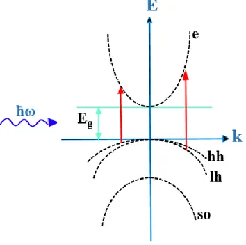
Band structure of III-V semiconductor compounds such as InAs shown in Figure 2.2. As we see three subbands in the valence band represent the p bonding states while the single conduction band corresponds to s antibonding orbital. The positive curve in the E-k diagram shows the electron band whereas, the three negative parabolas represent hole bands. Two of them are degenerate at k = 0 which are called heavy hole and light hole states. The other one is split-off hole band in a lower energy that is a consequence of spin-orbit coupling.
Bandgap is direct here which means that both of the valence band maximum and the conduction band minimum take place at k = 0 in the Brillouin zone. There is not a considerable change in wave vector to conserve momentum. Therefore interband absorption is presented by vertical arrows in the E-k diagram. However, in the case of indirect bandgap, minimum of the conduction band occurs at k≠0. As a result, not only a photon absorption but also, participation of a phonon is required for the transition to conserve momentum.
6
Figure 2.2 Schematic diagram of band structure of direct gap III-V semiconductors near to the center of Brillouin zone.
In quantum wells, electrons and holes are confined in one direction while they can move freely in the other two directions. The wave functions for a quantum well in which electrons and holes have free motion in x-y plane but are confined in z direction are given by:
To determine the wave functions and energies of quantized states in z direction we can model that with one dimensional potential well with infinite barriers as a primary case. We consider a quantum well with thickness of Lz in which the potential is zero for 0 ˂ z ˂ Lz and infinite elsewhere. The Schrödinger equation inside the well is:
( , , )x y z ( , ) ( )x y z 1.1 2 2 * 2 ( ) ( ) 2 n n z E z m z h 1.2
7
n
E
and
n are energy and wave function of nth solution of equation aboverespectively. ℏ is reduced Plank constant and m* is the effective mass of electrons. The solutions that satisfy boundary condition as φ=0 at infinitely high barriers are in the form of:
Quantum confinement in the z direction leads to quantization of energy levels
E
n andwave vectors
k
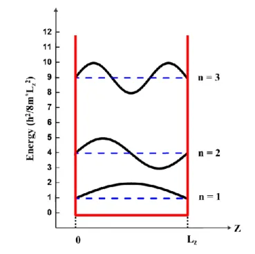
z. n is an integer which indicates quantum number of state.Figure 2.3 shows the first three wave function of infinite potential well. Confinement energies are proportional to n2 inunits of h2 / 8m L* z2 where n=1 is ground state and higher levels are excited states.
2 ( ) sin( ) n z z n z z L L 1.3 2 2 *( ) 2 n z n E m L h , z z n k L
1.48
Figure 2.3 First three energy levels and corresponding wave functions of an infinite potential well of width Lz.
2.2 Optical absorption of quantum wells
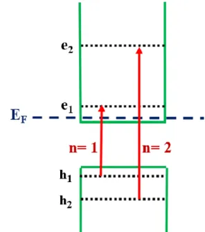
Here we study linear interband optical absorption of III-V quantum wells ignoring exitonic effects. When the light is radiated in the z direction perpendicular to the well, instead of conservation of momentum, selection rule will be considered because in this direction, energy states are quantized. Electron travels from initial state in the valence band to the final state in the conduction band by absorbing a photon. Absorption rate can be deducted through Fermi’s golden rule which is directly dependent to the density of states and squared matrix element. Matrix element includes dipole moment and electron-hole overlap integral [7]. Selection rule for an infinite quantum well indicates that transitions from nth hole band to the n՛ th electron band is allowed if only Δn = n՛ -n = 0. This follows from overlap integral consist of envelope wave functions of electron and hole states. Since we have sinusoidal standing waves for the well, overlap integral is nonzero if n՛ = n.
9
Figure 2.4 The first and second allowed interband optical transitions in accordance with selection rules in a quantum well.
However electrons and holes have discrete energy levels in the quantum well, they can move freely in the x-y plane of the well and have kinetic energy associated with the free motion. Therefore the total energy can be determined by following:
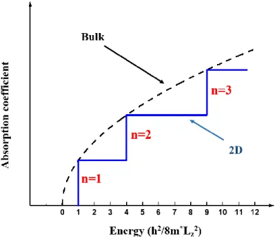
Since density of states of the motion in x-y plane is constant, it is stepwise for the discrete confinement energy levels. So the optical absorption of quantum well consists of steps with outset energies follows from quantized energies while each step corresponds to one quantum number.
2 2 2 2 *( ( ) ) 2 total x y z n E k k m L h 1.3
10
Figure 2.5 The step like absorption coefficient of an infinite quantum well of width Lz compared to the 3D case.
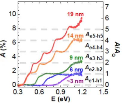
2.3 Quantum Optical absorption of InAs membrane
Optical absorption properties of InAs membranes with thickness Lz ̴ 3-19 nm on CaF2 substrate was studied by Fang et al [8]. Since bulk InAs has large Bohr radius, electrons and holes will be confined strongly in sub-20-nm thicknesses. InAs quantum membranes (QMs) sandwiched by air in one side and CaF2 of large bandgap on the other side behave like infinite potential wells. Therefore allowed interband transitions followed from selection rules are en-hhn (nth heavy hole subband to nth electron state) transitions and en-lhn (nth light hole subband to nth electron level) transitions. Fourier transform infrared (FTIR) is used to measure transmission (T), and reflection (R) of InAs QMs at room temperature. T is proportion of incident light transmitted through the membrane while R is the portion of light which is refracted from the membrane. The range of measurement was 2414-9656 cm-1 in which CaF2
11
is transparent. Using A+T+R=1 relation, optical absorptance (A) that is the portion of light absorbed by the sample has been calculated.
Experimental data shown in Figure 2.6 indicates that absorptance spectra of InAs QMs with different thicknesses are step like and each step’s amount is about 1.6 ± 0.2% resulting from quantized interband transitions.
Figure 2.6 Experimental absorption of InAs QMs of different thicknesses at room temperature. The magnitude of quantum absorptance AQ for each step is 1.6% and are shown by dashed lines. The Aen-hn indicates the absorption corresponding to the interband transition from nth hole state to the nth electron state [8].
Using Fermi’s golden rule, optical absorption coefficient h( )of an infinite
potential well with thickness of Lz can be obtained. For the incident electromagnetic wave with polarization vector ê and frequency ω shined perpendicularly to the well, the absorption coefficient is the following [9],
12
Where e is the charge of electron, μ is the reduced electron-hole mass( 1/1/me1/mh) ,
n
r is the real part of refractive index, c is the speed of light, 0is the vacuum permittivity, m0is the rest mass of electron, ħ is reduced Planck’s constant, and e pˆ.rcv 2is momentum matrix element. On the other hand, k.p perturbation theory results to 1/4 pcv/mo2/hwhich leads to cancel pcv2in the numerator. The simplified term left behind all of the cancelations is Lz (e2/ 40hc n) / rwhich is the absorption corresponding to each step where (e2/ 4
0hc)is fine structure constant (α) and it amounts 1/137.Like graphene, an atomically thin 2D material absorbs 2.3% portion of light [2]. However, the measured absorptance amount for each step (1.6%) is less than πα evidently. It means we need a correction since the quantum membranes are not free standing and lied down on a substrate therefore the refractive index of surrounding medium should be taken into account. Considering Fresnel law, the membranes with substrate of refractive index n reflect (1-n) / (1+n) portion of incident electric field E0 while the transmitted part is 2 / (1+n). Hence the optical absorption is decreased by {2 / (1+n)} 2 thus the correction factor will be n
c = {(1+n)/2)} 2 which is called the local field correction factor. The quantum absorption will be the following
Considering the refractive index of CaF2 n = 1.43, nc =1.48, the absorption step will be 1.58% which is consistent with experimental results with 3% error.
2 2 2 2 0 0 ˆ ( ) . cv r z e e p n c m L h r h 1.4 2 2 ( ) 1 Q c A n n
1.513
Chapter 3
Optical Properties of Graphene
After understanding the optics of 2D materials, we study optical properties of graphene. Unique band structure of graphene is the source of its distinct optical properties. Two optical contributions which give rise to optical absorption of graphene are interband and intaraband transitions. We can modify the optical transitions in graphene through doping. Broadband optical response of highly doped graphene which is grown by CVD technique and transferred on transparent substrate is investigated afterwards.
3.1 Electronic structure of graphene
The electronic band structure of graphene has been studied theoretically long before its existence [10].It can be derived using tight binding model. Graphene is formed by carbon atoms in a honeycomb lattice structure [11, 12]. An isolated carbon atom with electronic structure of 1s2 2s2 2p2 has four electrons in the outer shell called valence electrons which can make new orbitals through hybridization. The result is three sp2 orbitals from the interaction of s orbital with px and py leaving a pure p orbital pz. The hybridized sp2 orbitals are arranged in the xy-plane with 120º angles by ϭ bonding to
14
the three neighboring atoms. Therefore the output is a two dimensional honeycomb lattice with strong ϭ bonds. The energy gap between bonding and antibonding sigma orbitals is so large that electrons cannot participate in electrical conductivity of graphene. However the pz orbitals perpendicular to the plane give rise to the conductivity of graphene through π bonding and π* antibonding.
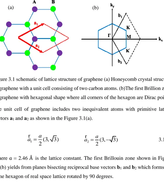
Figure 3.1 schematic of lattice structure of graphene (a) Honeycomb crystal structure of graphene with a unit cell consisting of two carbon atoms. (b)The first Brillion zone of graphene with hexagonal shape where all corners of the hexagon are Dirac points. The unit cell of graphene includes two inequivalent atoms with primitive lattice vectors a1 and a2 as shown in the Figure 3.1(a).
Where ɑ = 2.46 Å is the lattice constant. The first Brillouin zone shown in Figure 3.1(b) yields from planes bisecting reciprocal base vectors b1 and b2 which forms the same hexagon of real space lattice rotated by 90 degrees.
1 (3, 3) 2 a a r 2 (3, 3) 2 a a r 3.1 (a) (b)
15
The six corners of the first Brillouin zone are two inequivalent group labelled K and Κ′which are called Dirac points. Moving from K to Κ′ , there is the saddle-point singularity at M point. The center of Brillouin zone is Γ.
The dispersion relation of electronic bands in the nearest neighbor approximation of graphene has the form
Where
0 is the nearest neighboring hopping energy [13, 14]. kx and ky are x and y components of momentum. By plotting energy as a function of k according to equation (3.4), two curves will be obtained from which, the upper one is denoted by π* band and the lower one is called π band. The two bands are degenerate at Dirac points. Dirac point is also the Fermi energy level EF in intrinsic graphene. There are two atoms in unit cell of Brillouin zone therefore their two electrons will fill the π band and leave the π* band empty. The filled π band noted as valence band and the empty conduction band (π* band) resemble semiconductor structure with a major difference that in graphene the bandgap is zero. Since the Fermi energy corresponds to E± (k) = 0 at Dirac point, by expanding equation (3.4) around Fermi level we acquire the linear dispersion relation.1 2 (1, 3) 3 b a r 2 2 (1, 3) 3 b a
r 3.2 𝚱 =2𝜋 3𝑎(1, 1 √3) 𝚱 ′=2π 3a(1, − 1 √3) 3.3 0 23
( )
1 4 cos(
) cos(
)
4 cos (
)
2
2
2
y y xk a
k a
k a
E k
3.416
Where Vf 30a/ 2h ≈ 106 m/s is the Fermi velocity of Dirac fermions. It can be deduced from equation (3.5) that electrons in graphene behave as massless particles considering the effective mass as derivation of energy with respect to k.
3.2 Doping of graphene
Doping can modulate electrical and optical properties of graphene effectively. There are different methods to dope graphene in order to tune its charge carrier’s concentration. Electrical gating such as back-gating, top-gating or electrolyte gating can dope graphene by applying the gate voltage. However, chemical doping including substitutional doping and surface transfer doping controls charge carrier density of graphene by exploiting chemical species. In this study, we used electrolyte gating and surface transfer doping techniques. Electrolyte gating is applied in this chapter while surface transfer chemical will be considered in chapter 4.
Electrolyte gating is an electrostatic doping method applied for optoelectronic devices. This is done on supercapacitors with electrolyte between graphene and a metal electrode. The electrolyte liquid carries mobile ions which get polarized by applying a voltage. As a result, a few nanometer-thick electrical double layer (EDL) are generated at the graphene and metal electrode’s surfaces shown in Figure 3.2.
17
Figure 3.2 Electrolyte gating method of graphene. Applied gate voltage generates an electrostatic potential difference between the gold electrode and the graphene. Fermi energy is shifting by increasing charge carriers through electric field.
The charged ions of EDL induce electric fields which change the carrier density up to 1014 cm-2 corresponding to about 1 eV Fermi energy. The drawback of this method is electrochemical window of the electrolyte to obtain high charge carrier density on graphene. Narrow electrochemical window of electrolyte can restrain concentration of charge carriers and shifting Fermi energy of graphene. Here we used the ionic liquid which has a wide electrochemical window enabling us to shift Fermi energy of graphene to a greater extent than 1eV.
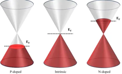
When electrons are added to the conduction band of graphene, it is called n-doped, while addition of holes to the valence band of graphene leads to p-doped graphene [15].
18
Figure 3.3 Graphene’s Dirac cones in three different cases. P-doped graphene is obtained by introducing holes to the graphene and therefore, Fermi energy shifted down. In the pristine graphene, Fermi level is at the Dirac point. The n-doped graphene is electron injected and Fermi energy is shifted up.
3.3 Optical properties of graphene
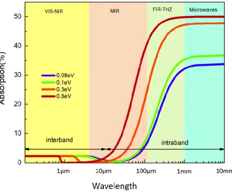
Strong interaction of light with graphene extends over wide range of frequencies from UV and visible to far infrared and terahertz regions [16-18]. Two different types of optical transitions induce optical absorption of graphene. For high energy photons, optical absorption of graphene is dominated by interband transitions which is frequency independent and has a constant universal amount πα ≈ 2.3%. This transition appears in visible and near infrared ranges. However intraband transitions
19
dominate at low energy photon ranges such as far infrared and terahertz that electrons can only move within bands.
Figure 3.4 Wide-range optical response of graphene illustrated from visible to microwave spectrum. Graphene absorbs 2.3% of light at visible-near infrared region in which interband transitions arise from high energy photons. However, the absorption reaches 50% due to intraband transitions for low energy photons at terahertz and microwave area.
Both of these optical contributions depend totally on fermi energy of graphene. During the doping process, Fermi energy is shifted and consequently the cut-off frequency of interband transitions shifts to higher energies; however, the amount of absorption remains constant. Even so, in the intraband contributions, the high level of doping increases the number of free carriers and enhances the absorption. Figure 3.4 presents the modelling of optical absorption of monolayer graphene and its
20
broadband response to electromagnetic waves. Optical absorption of graphene can be tuned by shifting Fermi energy through electrostatic gating or chemical doping. 3.3.1 Interband optical transitions
The incident light to the graphene can excite electrons to travel from valence band to conduction band leaving holes illustrated in Figure 3.5(a). These transitions are called interband transitions and they take place when a photon has enough energy to provide for the band to band transition of an electron. The photon energy should be at least twice the Fermi energy of graphene with respect to cone tip to be capable of creating electron-hole pair.
Figure 3.5 Interband transitions. (a) A photon with energy of 2EF or more is absorbed by an electron exciting it from valence band to conduction band. (b) Optical transitions for energies less than 2EF are blocked.
When graphene gets doped, the Fermi energy is shifted. Due to Pauli Exclusion Principle, interband optical transitions are not allowed at energies below 2EF, shown in Figure 3.5(b). Therefore it is called Pauli blocking. In the Pauli blocking region, photons with energy less than 2EF cannot excite electrons, therefore, banned optical transitions lead to vanishing the optical conductivity of graphene.
21
Graphene’s remarkable properties rest on its optical conductivity derived from Kubo formalism [19]. The graphene conductivity consists of interband and intraband conductivities which are complex functions. The real part of interband conductivity for the graphene with Fermi energy of EF at temperature T is frequency dependent as following:
Where ω is the angular frequency of the incident photon, h is the reduced Planck’s constant, kB is the Boltzmann constant and
2 0
e
/ 4
h
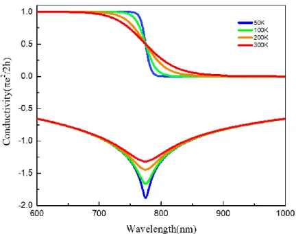
[2] is the universal conductance of graphene. The imaginary part of interband conductivity is frequency dependent as well and is expressed as:The complex interband conductivity of graphene for different temperatures is shown in Figure 3.6. The stepwise part of the plot illustrates the real interband conductivity which demonstrates the interband optical absorption while the other one presents the imaginary part of the conductivity [20].
0 int 2 2 Re {tanh( ) tanh( )} 2 4 4 F F er B B E E k T k T
h h 3.6 2 0 int 2 ( 2 ) Im { } 2 ( 2 ) (2 ) F er F B E ln E k T h h 3.722
Figure 3.6 Modeled real and imaginary parts of conductivity of graphene at different temperatures. Both parts are temperature dependent.
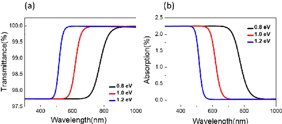
The stepwise optical absorption of graphene shown in Figure 3.7 (b) is calculated at different Fermi energies. This behavior comes from the real part of optical conductivity. A(ω) = (4π/c)Reσ(ω) = πα shows the relation between interband optical conductivity and absorption. T = (1 +πα/2)-2 ≈ 1 – πα = 97.7% gives the transmittance of graphene in the visible region [21]. As the reflection of graphene in this range is negligible, the optical absorbance of graphene will be A = 1 – T ≈2.3%.
23
Figure 3.7 Optical spectrum of graphene at different Fermi energies in visible range. (a) Transmittance of graphene is about 97.7% in visible range (b) absorption spectrum of graphene is about 2.3% for energy photons of 2EF . Therefore, by increasing Fermi energy, transition of photons with less energy is blocked.
The optical spectrum of graphene in visible range indicates the constant absorption of 2.3% . When Fermi energy of graphene shifts through doping, optical transitions for energies below 2EF are blocked and absorption goes to zero in that frequency range as shown in Figure 3.7.
3.3.2 Intraband electronic transitions
The optical response of graphene in far infrared and terahertz ranges in which, photons have low energies, is mainly controlled by intraband transitions. The optical absorption in this area, is noticeable and is contained by free carrier response. When photons excite carriers between the levels inside the valence or conduction band, intraband transitions take place. For instance, absorption of photons can excite electrons from an occupied level under the Fermi level to an empty state over EF. To conserve energy and momentum, the process should include either phonon scattering or defect scattering as an intermediate state.
24
Figure 3.8 Low energy photons in the conduction band can excite electrons within the band called intraband transition.
When the density of free electrons in the conduction band is increased, the intraband carrier transition increases which is followed by a dramatic increase in the absorption shown in Figure 3.8. This holds true also for the excess density of free holes in the valence band. The free carrier optical absorption of graphene can be described by Drude model in which, the excited electrons collide with phonons and impurities and get scattered afterwards. The frequency dependent conductivity with the electron scattering time τ is as the following [22, 23],
Where
dc
e E
2 F
/
h
2 the dc conductivity [5], ω is the angular frequency of light and e is the charge of electron. The separated real and imaginary parts of intraband conductivity are:( )
1
dci
3.825
The diagram of equations above is shown in Figure 3.9 (a) and 3.9(b) for different quantities of Fermi level.
Figure 3.9 Intraband conductivity (a) Real part of Drude conductivity at different Fermi energies. (b) Imaginary Drude conductivity of different Fermi energies.
3.4 Synthesis of graphene
Graphene was first fabricated from bulk graphite using scotch tape by mechanical exfoliation [15].This method provides graphene with high carrier mobility but the large area graphene cannot be obtained. There are other methods such as growing graphene on SiC substrates by epitaxy, annealing solid carbon sources and chemical vapor deposition (CVD). During CVD technique, the gas-phase precursors accumulated on the surface react and lead to the deposition of a thin layer following from chemical reactions in high temperature and low pressure. In the case of graphene, CVD method is the promising way to produce large area graphene in a low
2 2
Re ( )
1
dc
, Im ( ) 2 2 1 dc
3.8 (a) (b)26
cost [24]. Carrier mobility of CVD graphene is lower compared to graphene yielded from exfoliation method [25], however, it can be improved by optimization [26]. CVD method can be applied to grow both monolayer and multilayer graphene. For the single layer growth of graphene, we use copper substrate since it is an effective catalyst to transform hydrocarbons into graphene and its carbon solubility is negligible even in high temperature therefore it is more likely to have a monolayer coverage of graphene on copper’s surface.
Figure 3.10 (a) Quartz chamber is placed in the furnace and the temperature of furnace can rise up to 1070 degrees. (b) Cu foils are cut and arranged on the holder. The CVD system used in our lab, consists of a quartz chamber settled in a furnace including gas sources, a mechanical pump to vacuum the chamber and units to control gas flow.
27
Figure 3.11 (a) Vacuum Gauge showing that chamber is pumped down to a vacuum of 6 mTorr. (b) Mass flow controllers showing flow amount of hydrogen and methane.
As substrates, the ultra-smooth copper foils of thickness 20 μm were cut in 1x2.5 cm2 sizes and put on the quartz holder of size 7x30 cm2 and placed in the chamber. The chamber was then evacuated to 6 mTorr shown in Figure 3.11(a). Then copper substrates were heated under hydrogen H2 flow with rate of 100 sccm until the temperature reached 1035 ºC. It is applied to remove the oxide layer and other chemical residues from the surface of the copper substrates. When the chamber reached 1035 ºC, the growth of graphene was initiated by flowing methane CH4 at a rate of 10 sccm for one minute shown in Figure 3.11(b). During the deposition, a chiller cooled down the edges of the system to avoid damage to the gasket materials. After closing methane flow, the system was cooled down to the room temperature under hydrogen flow. Then the chamber was opened to air to unmount the samples.
28 3.5 Transfer procedure
The CVD graphene is advantageous since it can be transferred to different sorts of surfaces depending on device type and the desired application area. We transferred graphene onto solid substrates such as glass and quartz and flexible surfaces such as PVC and polyethylene.
To transfer graphene to one of the aforementioned substrates, firstly the graphene on ultra-smooth copper foil with 20 μm thickness was covered by photoresist (Shipley 1813) shown in Figure 3.12(a). The samples were put in the oven 60 ºC and baked for 24 hours. Afterwards, the copper was dissolved using wet etching. For this purpose, Iron chloride (FeCl3) was used as the copper removing solution. This solution leaves chemical residues on graphene which are difficult to clean. Therefore, a solution of Nitric acid, Hydrogen peroxide, Hydrochloric acid and water was used as copper etchant. The consequent graphene had higher quality and was less contaminated, although, the resultant graphene got chemically doped by Nitric acid. As the last step of the process, the graphene on photoresist was placed on the substrate with graphene facing the surface of substrate. Figure 3.12(c) Illustrates the sample of graphene on photoresist put on polyethylene which placed on a hotplate. The sample was heated up to 90 ºC to let the graphene layer stick to the substrate. Then the photoresist was removed by acetone. Then the substrates were further cleaned by isopropyl alcohol (IPA). Graphene on polyethylene is shown in Figure 3.12(d).
29
Figure 3.12 Graphene transfer process. (a) Photoresist (PR) on CVD-deposited graphene on Cu. (b) The baked sample in the etchant to remove Cu. (c) Graphene on PR placed on the polyethylene substrate and heated on a hotplate. (d) Graphene on polyethylene where the PR is removed by acetone.
Lamination is another method that we used to transfer graphene. This technique is advantageous for large area graphene. Although we are limited by the size of chamber and holder, there are optimized cylindrical holders through which, graphene samples of the size 30x30cm2 can be obtained. The first step of lamination method is to place on-copper foil-deposited graphene onto the substrates such as polyethylene or PVC
PR
(a) (b)
Etchant
(d) (c)
30
(polyvinyl chloride) where the graphene faces PVC. The sample with is protected on both sides by laminated paper using laminating machine. Then as we mentioned before, the copper was etched by solvent. Shown in Figure 3.13(b), we applied tapes at the edges of the sample to create copper stripes as electrical contacts.
Figure 3.13 Graphene transferred on PVC by lamination. (a) Lamination machine used to laminate CVD graphene on the PVC substrate. (b) Laminated graphene where graphene is between the PVC and Cu. (c) Cu removed by iron chloride to leave graphene on PVC. The tapes used to avoid Cu etching on the sides to take contact from graphene. (d) The conductance of graphene on PVC in kilo ohm.
Graphene on Cu PVC Lamination machine Graphene on Cu laminated on PVC (b) (c) Etchant Graphene on PVC (d)
31
3.6 Optical response of highly doped graphene
Pristine graphene has frequency independent conductivity of
which gives rise to the frequency independent transmittance that is formulated as
Where α is the fine structure constant [12, 18, 27]. Nevertheless, the optical response of graphene is highly frequency dependent at low photon energies since it is controlled by free-carrier absorption. Drude conductivity model can explain optical response of graphene in far-infrared region. The sheet conductivity is in the form of
Where,
dcis the dc conductivity and τ is the scattering time of electron. DrudeweightDdc /can express the Drude conductivity for microscopic factors. Drude weight has the form of 2
F
De n for graphene where, VF is the Fermi velocity of 106 m/s and n is the concentration of charge carriers [22, 28].
2 (1 ) 1 0.977 2 T 3.10 ( ) 1 dc i
3.11 2 0 e / 4 h32
Figure 3.14 schematic of device structure. The device is composed of gold electrode, graphene on a substrate and ionic liquid in between as a gating medium. By applying voltage, ionic liquid gets polarized generating ELD and induce electric field.
An effective device structure of a supercapacitor enabled us to investigate and manipulate optical properties of graphene [29, 30, 31]. We fabricated a capacitor that is composed of graphene and gold electrode with a layer of electrolyte in between shown in Figure 3.14. A monolayer graphene was deposited on copper and transferred onto porous polyethylene with the thickness of 20μm. Gold electrode was fabricated by evaporating 60nm thick gold on a PVC substrate. Then a circular window with 6mm diameter was opened as the optical window for the incident beam. Porous polyethylene is transparent in far infrared region. The porosity of polyethylene makes electrolyte hold on to it. Polyethylene with absorbed electrolyte is also transparent up to visible range.
33 Figure 3.15 The FTIR spectrometer setup
The light radiated from the source goes through the beam splitter and is splitted into two beams one of which, is reflected to the fixed mirror and the other is transmitted to the movable mirror. The moving mirror changes the total path length compared to the fixed mirror. Then the two beams bounce back from the fixed and movable mirror back to the beam splitter and recombine. Since the length paths are varied, they generate constructive and destructive interferences that is called interferogram. The beam goes through the sample and all the wavelength characteristics of the sample’s spectrum get absorbed thus these wavelength are deducted from the interferogram. Therefore, energy difference during time for all the wavelengths is determined by the detector. The resultant interferogram is translated by Fourier transform algorithm. Since time and frequency are reciprocal, Fourier function gives the intensity versus frequency instead of time.
Bruker’s V70x Fourier-Transform Infrared spectroscopy system used in this study which has a wide range source and corresponding detectors. To measure the spectrum (transmission, absorption or reflection) of a given device, we place it in the
34
compartment. The charge neutrality point was taken as the gate voltage reference where the dc conductivity is minimum and charge density is zero.
In order to find the reference, first the capacitance and resistance of the device was measured. Using this approach, the charge neutrality point (VCN) or Dirac point is probed by finding the point at which, the capacitance value is the lowest and resistance is the highest. Dirac point is dynamic and can change by different gating configurations. If the graphene is grounded while applying positive voltage to the gold, electrons are generated on the surface of the graphene. In this configuration, if the applied voltage is scanned from the Dirac point (1 V here) through negative voltages, holes are induced on graphene (hole-doped device) while in the case of positive voltages, electrons would be generated (electron-doped device).
Figure 3.16 To Find the Charge neutrality point (a) Capacitance and (b) Resistance of graphene device vs gate voltage is measured.
The Fermi energy of graphene for different gate voltages can be extracted from the visible and NIR cut-off wavelengths. In this regard, the transmission of the devices were measured in the visible and NIR ranges for both the electron and hole doping regimes.
35
Figure 3.17 Normalized transmittance of graphene device at visible for (a)electron doping regime and (b)hole doping regime of different Fermi energies.
The absorption of free standing graphene is 2.3%in the visible through NIR ranges, although it decreases for graphene on dielectric substrate if the refractive index of the substrate is taken into account. The polyethylene with ionic liquid is transparent at visible range with a refractive index of about 1.6. Therefore, the absorption is calculated to be about 1.4% using equation 2.5. Since reflection in this range is negligible, transmittance is nearly equal to absorption subtracted from unity. This is almost in agreement with the experimental measurements in Figure 3.17 where absorption is 1.5%.
Fermi energy of graphene can be extracted at different gate voltages using Pauli blocking principle. At high energy photons, electrons absorb enough energy to excite from valence band to conduction band leaving holes. When fermi energy is shifted to higher energies, the transitions for photons with energies less than 2EF energy barrier, are blocked. 2EF at each gate voltage equals to the corresponding cutoff wavelength.
36
Figure 3.18 represents the calculate Fermi energies at visible range using spectrum of Figure 3.17 for both hole and electron doping.
Figure 3.18 Extracted Fermi energies of different gate voltages from cutoff wavelength.
Transmittance spectrum of graphene device at NIR-MIR range shown in Figure 3.19 is only measured for electron doping regime.
Figure 3.19 Differential transmittance of graphene device at near and mid infrared for electron doping regime.
37
The oscillations in the transmission spectrum is due to multiple reflection between graphene and gold surfaces. Portion of light transmitted from graphene layer reaches the gold electrode which results in multiple short beams that interfere with each other. It leads to the multiple transmission which is indicated as oscillations in the transmission spectrum.
FTIR spectrometer can measure optical response of graphene at low frequencies using far infrared source and wide range detector which can go down to 50cm-1 wavenumber or 1.5 terahertz.
Figure 3.20 Terahertz transmittance spectrum of graphene device at electron doping regime.
At this range, the optical response of graphene is controlled by free carriers. Low energy photons simulate hot carriers within the band thus, increasing the concentration of free carriers through doping enhances intaband transitions therefore optical absorption intensifies. The suppression of transmittance in Figure 3.20 indicates the dramatic raise of absorption in this range.
38
Chapter 4
Optical
residual
absorption
of
graphene
4.1 Introduction
The electronic band structure of graphene indicates that interband excitations of electrons for energy states below 2EF are banned. Due to Pauli’s exclusion principle, only photons with energies higher than 2EF can excite electrons and create electron-hole pairs. Therefore the optical absorption of graphene is expected to drop to zero for energies below the 2EF threshold. However, a considerable absorption below 2EF has been reported [6]. The optical absorption measured in Pauli-blocked region is called optical residual absorption. The residual absorption may follow from both internal and external effects. Charged impurities and structural defects such as vacancies, wrinkles and cracks are the external causes which can lead to residual absorption. In a theoretical study, the effects of charged impurities and unitary scatters (vacancies, cracks, edge defects, etc.) on the infrared optical response of graphene has been examined and a considerable amount of optical conductivity in the
39
energy region below 2EF was found [32, 33]. Reference (32) indicated that disorders extend energy levels and increase density of states at Dirac point which means that the Pauli exclusion cannot block transitions efficiently and even for energies below 2EF, there are still some transitions. The internal source of the residual absorption is explained in terms of many-body interactions like electron-electron, electron-phonon and electron-hole interactions. For instance, e-e and e-ph interactions increase the scattering rate of charge dynamics of graphene in infrared region. The frequency dependent scattering rate gives rise to an increase in the optical conductivity in comparison with Drude model. The strong excitonic effect pronounced in the optical response of graphene indicates the decreased screening of e-e interactions and zero density of states at the Dirac point [34]. Here we investigated optical residual absorption of graphene at visible and near infrared region. First, the optical response of single layer graphene at the linear dispersion regime was studied theoretically by transfer matrix method. The band to band transition and excitonic effect were included in the model afterwards. Then, details of experiment followed by spectroscopy of optical response of graphene and discussion has been demonstrated.
40 4.2 Simulation of monolayer graphene
Optical response of a single layer graphene can be deducted using transfer matrix method formulated by Zhan et.al [35]. It is based on the fact that the electric or magnetic fields of two media can be related to each other through transfer matrix. Two types of transfer matrices are transmission matrix and propagation matrix.
Figure 4.1 Schematic of optical response of monolayer graphene with conductivity of ϭ sandwiched between two dielectric media with dielectric constants of ε1 and ε2. Forward and backward propagating electromagnetic waves with field coefficients of a1, a2, b1 and b2, respectively.
A single layer graphene with optical conductivity ϭ surrounded by two dielectrics is illuminated with light shown in Figure 4.1. The dielectric constant of the two dielectric media are ε1 and ε2 assuming that light is propagating in z direction. The connection between fields crosswise the interface is through transmission matrix. When the light is polarized in y direction, the magnetic field for p polarization is the following
41
Where, a1 and a2 are field coefficients for the forward propagation while, b1 and b2 are correlated to backward propagation.
k
ix andk
iz are x and z components ofwave vector ki i /c and,
k
1x
k
2xdeducted from Snell’s law. Subsequently,electric field E can be determined fromEi
0 i(kˆiHi)r r
presented in equations (4.3) and (4.4). μ0 is the vacuum permeability and, νi is the phase velocity of the electromagnetic wave.
Where,
0is vacuum permittivity. We apply following boundary conditions for electric and magnetic field at z = 0 to obtain transmission matrix. The surface normal is ˆn . zˆWhere J is the surface current density. By substituting the equations of electric and magnetic fields in boundary condition expressions we are left with following,
1 1 1 1 ( 1 1 ) x z z ik x ik z ik z y H a e b e e , z < 0 , 4.1 2 2 2 2 ( 2 2 ) x z z ik x ik z ik z y H a e b e e , z > 0 4.2 1 1 1 1 1 1 1 0 1 0 1 ˆ z z ik z ik z z z a b E k e k xe
r , z < 0 4.3 2 2 2 2 2 2 2 0 2 0 2 z z ik z ik z z z a b E k e k e
r , z > 0 4.4 2 1 0 ˆ ( ) z 0 n Er Er 4.5 2 1 0 ˆ ( ) z n Hr Hr Jr 4.642
Combination of equations (4.7) and (4.8) can connect the field coefficients through the transmission matrix D12 as
Where the transition matrix is
With the matrix element’s parameters as
In the case of s polarization, electric field is in y direction and the transmission matrix can be calculated as well. Since we study the case of a single layer graphene with two surrounding dielectric media interacting with electromagnetic wave, the transmission matrix is the transfer matrix M = D12. Therefore the elements of transfer matrix can yield the reflection coefficient r and transmission coefficient t of a monolayer graphene as 2 1 2 2 1 1 2 1 ( ) ( ) 0 z z k k a b a b
4.7 2 1 1 2 2 0 2 2 0 2 ( ) ( ) z ( ) x x z k a b a b J
E
a b
4.8 1 2 12 1 2a
a
D
b
b
4.9 12 1 1 1 1 D 4.10 1 2 2 1 z z k k
, 2 0 2 z k
. 4.1043
Thus the reflectance R and transmittance T will be in the form of,
Absorption can be obtained from
Here we consider optical response of single layer graphene in visible and NIR region in which, the optical absorption of graphene is associated with interband transitions. The optical conductivity of pristine graphene is frequency independent in this range and is equal to πe2/2h called universal conductance of graphene where, h is Planck’s constant and e is the electron charge. The absorption corresponding to this conductivity is obtained by A( ) (4/ ) ( )c which equals to πα ≈ 2.3%. Figure 4.2 demonstrates the transmittance, reflectance and absorptance spectrum of free standing graphene calculated at different Fermi energies. As we expect, the reflectance of graphene shown in Figure 4.2(b) is negligible and absorption is about 2.3%.
(2,1)
(1,1)
M
r
M
,1
(1,1)
t
M
4.11 2 R r , T t2 4.12 1 A T R 4.1344
Figure 4.2 Optical response of free standing graphene at different fermi energies. (a) Transmittance of graphene is about 97.7% considering negligible reflectance yields 2.3% absorption. (b) Reflectance spectrum of graphene is inconsiderable and does not have significant effect on the graphene’s absorption. (c) Absorption of graphene is about 2.3% in this region.
While Fermi energy of graphene shifts through doping, absorption remains constant. By shifting Fermi energy, the transitions for energy photons below 2EF is not allowed due to Pauli blocking principle. In Figure 4.2, shifting of Fermi energy to higher frequencies is noticeable.
However, the absorption of graphene transferred on a substrate is not 2.3% any longer. Therefore the correction factor (2/n+1)2 should be included. Accordingly, absorption is calculated by A
(2 /n1)2 where, n is the refractive index of the substrate. Figure 4.3 represents the optical response of graphene on a substrate with refractive index of n = 1.5 at different Fermi energies. A simple calculation results in an absorption of 1.47% for this case. The absorption of graphene in our model is around 1.56% which is in close agreement with the theory.45
Figure 4.3 Optical spectrum of graphene on a dielectric substrate with refractive index of n = 1.5. (a) 91.7% of transmittance is calculated which is decreased compared to the transmittance of free standing graphene. (b) Reflectance is increased to 6.7% and (c) Graphene’s absorption is decreased to 1.57% due to refractivity of the substrate.
All the calculations above have been considered near Dirac point where, dispersion relation is linear. In the linear dispersion region, the optical conductivity of graphene is frequency independent and determined by fine structure constant. However the optical conductivity deviates from the universal conductance πe2/2h expected by independent particle model. At higher energy photons, a marked resonance feature is observed which is due to band to band transitions near the M point, the saddle-point singularity of Brillouin zone [34]. The resonance feature at UV is predicted as a symmetric peak at 5.20 eV within independent particle calculations. However the experimental optical conductivity shows an asymmetric peak at 4.62eV (268nm). The large redshift of about 600meV can be explained by taking into account electron-hole interaction role in the optical response of graphene near the M point. Coupling of band to band transition near saddle-point singularity and excitonic effect leads to an asymmetric resonance feature which is in a good agreement with experimental results. Since there is not any analytical expression for interband conductivity of graphene including both resonance feature near saddle-point singularity and excitonic correction, we used the extracted conductivity of graphene from calculated data of reference (34) Figure 4.5 demonstrates the absorption of graphene on the substrate