A NEW DIFFERENTIAL CONFIGURATION
SUITABLE FOR REALIZATION OF HIGH
CMRR, ALL-PASS/NOTCH FILTERS
SHAHRAM MINAEI
1, İ.CEM GÖKNAR
1, OGUZHAN CICEKOGLU
21. Dogus University, Department of Electronics and Communication Engineering, Acibadem, 34722, Istanbul, TURKEY.
E-Mail: [email protected] www3.dogus.edu.tr/sminaei
Tel: +90-216-327 11 04
2. Bogazici University, Electrical and Electronics Engineering Department, Bebek, 80815, Istanbul, TURKEY.
E-Mail: [email protected] www.ee.boun.edu.tr/cicekoglu.html
Fax: +90-212-287 24 65
Abstract: In this paper, a new configuration suitable for realization of differential input-differential output first order, second order all-pass and notch filters with high CMRR is given. The proposed configuration uses two negative type second-generation current conveyors (CCII-), and three admittances. Two first order and one second order all-pass filters and a notch filter (tunable if current controlled conveyor CCCII is used) are extracted from the proposed configuration. Tracking error, element mismatch, sensitivity analysis, simulation and experimental results are included.
1. INTRODUCTION
All-pass filters, also called phase equalizers are widely used for phase shifting while keeping the amplitude of input signal constant over the frequency range of interest. They can be used to equalize the undesired phase change as a result of processing the signal; they can also be used in the synthesis of multiphase oscillators. Notch filters on the other hand are used to eliminate a single frequency called the notch frequency.
Several all-pass and notch filter realizations using active elements are available in the literature [1-18]. These circuits use active elements such as second-generation current conveyors (CCII) [1-7, 9-11, 15, 17], operational amplifiers [12, 17], current differencing buffered amplifiers (CDBA) [13], four terminal floating nullors (FTFN) [8,14], third-generation current conveyors (CCIII) [16, 18] together with passive elements. However all of these phase equalizers are single input-single output structures [1-18].
Due to recent advances in integrated circuit technology it is possible to place analog as well as digital components on the same chip, thus obtaining mixed–mode signal processing circuits. Mixed-mode signal processing attracts increasing attention since it simplifies design, enables compactness and reduces cost. However signal interference from the digital to the analog part remains a serious problem to overcome; hence, for such circuits differential building blocks are accepted as a good solution. Therefore it is desired to process signals in differential form rather than simply as referenced to ground. Another advantage of differential operation over the single-ended case is that the amplitude of the signal increases by a factor of 2 [19].
An important parameter of differential active structures is the common-mode rejection ratio (CMRR). Differential signals have the advantage of canceling common-mode interference from unwanted signals and/or noise.
This paper presents a general configuration for realizing differential-input differential-output voltage-mode all-pass/notch filter circuits in Section 2; it consists of two CCIIs and three
admittances and, has very high CMRR, independent of matching element values. In Section 3, two first order, one second order all-pass and notch low sensitivity filter circuits are derived. In all of the filter circuits the CCIIs can be replaced by a current controlled conveyor (CCCII); one of these filter circuits has only external capacitors, which makes it much more feasible for IC implementation. For all the circuits the pole frequency can be controlled electronically by adjusting the bias currents of the CCCIIs without disturbing the unity gain of the filter. The advantages of the configuration are exhibited by considering the effects of the tracking error and element mismatch on the output, CMRR and differential gain, in Section 4. Section 5 contains comparative simulation results of all the filter circuits using transistor level implementation for the current conveyors. In Section 6 two of the proposed filters are constructed practically, while Section 7 concludes the paper.
2. THE PROPOSED CONFIGURATION
CCII has become very popular because of its high performance coupled with functional versatility. It has led to a wide application for implementation of high performance electronic functions operating in voltage mode or current mode [20].
The circuit symbol of CCII is shown in Fig. 1 and its terminal relations in expression (1):
z x y z x yV
I
V
I
V
I
0
1
0
0
0
1
0
0
0
(1)Figure 1. Circuit symbol of the CCII.
The symbol of the CCCII
proposed in [21] is shown in Fig. 2 and is characterized by: z x y x z x y V I V R I V I 0 1 0 0 1 0 0 0 (2)
Figure 2. Circuit symbol of CCCII.
Here the parasitic resistance R is the input resistance at terminal X and for BJT realizations it x
can be expressed as o T x I V R 2 (3)
where VT is the thermal voltage and I0 is the bias current of the CCCII [21].
Conventionally the + or signs of IZ in equalities (1) and (2) denote the positive and negative
type of current conveyors respectively.
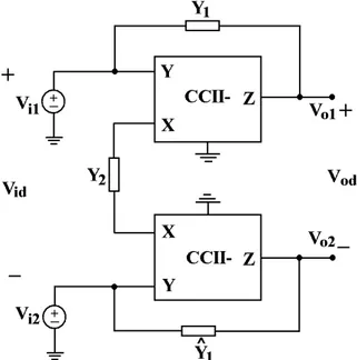
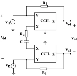
The proposed general differential configuration is presented in Fig. 3. The differential input is connected to the Y terminals of the conveyorsand the differential output voltage is taken across the Z terminals.
Figure 3. Proposed differential configuration. Defining Vid Vi1Vi2, 2 2 1 i i ic V V
V , and Vod Vo1Vo2, routine analysis of the circuit yields
the outputs as:
id ic o V Y Y V V ) 2 1 ( 1 2 1 (4)
id ic o V Y Y V V ) ˆ 2 1 ( 1 2 2 (5)
Then the differential output is:
id o o od V Y Y Y Y Y Y Y V V V 1 1 1 1 2 1 1 2 1 ˆ ) ˆ ( ˆ (6)
If the output V is expressed in terms of od V and id V as ic ic cm id dm od A V A V V (7) then, 1 1 1 1 2 1 1 Yˆ Y ) Yˆ Y ( Y Yˆ Y Adm (8) and 0 cm A (9)
are obtained. Note that the common-mode gain (Acm) of the circuit is equal to zero,
independent of passive elements mismatches. Therefore the common-mode rejection ratio of the filter can be found theoretically as
cm dm A A CMRR 20log10 (10)
which implies that the circuit has potentially high CMRR.
3. FILTER CIRCUITS DERIVED FROM THE CONFIGURATION
From the proposed differential configuration given in Fig. 3, different realizations for all-pass and notch filters can be extracted.
3.1. First Order All-Pass Sections
If in Fig. 3, the admittances are taken to be
1 1 1R Y , 1 1 1 ˆ R Y and 2 2 2 1 1 sC R Y then the
Figure 4. High CMRR first order RC All-Pass Filter. Single ended and differential outputs of the circuit are obtained as:
) 1 ( 2 ) 2 ( 1 ) 1 ( 2 2 2 1 2 1 Cs R V Cs R R V Cs R V ic id o (11)
) 1 ( 2 ) 2 ( 1 ) 1 ( 2 2 2 1 2 2 Cs R V Cs R R V Cs R V ic id o (12) id od V Cs R Cs R R V 2 2 1 1 ) 2 ( 1 (13)By expressing the output V as given in (7) od
Cs R Cs ) R R ( Adm 2 2 1 1 2 1 (14) and 0 cm A (15)
result. Selecting R1=R2=R the differential transfer function reduces to
RCs RCs V V id od 1 1 (16) and the filter has the following phase response
) arctan( 2 ) ( CR (17)
Equation (16) implies that the proposed circuit realizes transfer functions of a first order voltage mode all-pass filter with a gain of unity in magnitude. From equation (17) it can be seen that the circuit yields a phase shift from 0o to -180o.
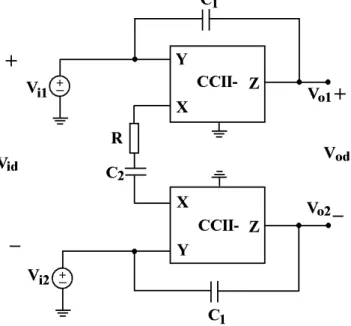
By RC-CR transformation, namely letting Y1 sC1, Yˆ1 sC1 and
2 2 1 1 sC R Y in the
configuration shown in Fig. 3, a new first-order all-pass filter can be obtained as shown in Fig. 5.
Figure 5. High CMRR first order filter after RC-CR transformation. Routine analysis of the circuit shown in Fig. 5 yields for the outputs of the circuit
) 1 ( 2 2 ) 1 ( 2 2 1 2 1 2 1 2 1 1 s RC C V Rs C C C C V s RC C V ic id o , (18)
) 1 ( 2 2 ) 1 ( 2 2 1 2 1 2 1 2 1 2 s RC C V Rs C C C C V s RC C V ic id o , (19) and id od V s RC s RC C C V 2 2 1 2 1 1 2 (20)for the differential output. Then differential and common mode gains are:
s RC s RC C C Adm 2 2 1 2 1 1 2 (21)
and
0
cm
A (22)
Note that the common-mode gain (Acm) of the circuit is always equal to zero. Selecting C1=C2=C
the differential transfer function reduces to
RCs RCs V V id od 1 1 (23) and the filter has the following phase response
) arctan( 2 180 ) ( CR (24)
From (23) and (24) it can be seen that the circuit realizes a first order voltage mode all-pass filter with a gain of unity in magnitude and yields a phase shift from 180o to 0o.
The pole frequency for both circuits shown in Figs. 4 and 5 is found as:
RC fp
2 1 (25)From equation (25) one can realize that the pole frequency can be adjusted by changing the value of the capacitor C or the resistor R without disturbing the unity gain of the phase equalizer. Moreover the sensitivity of the pole frequency is:
S
Rfp
S
Cfp
1
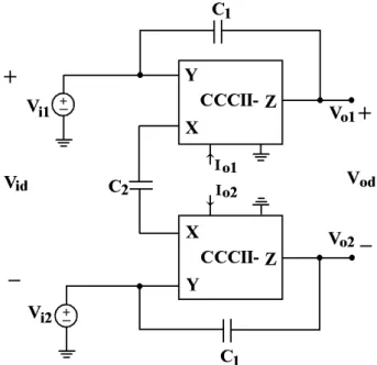
.In order to obtain a circuit more suitable for IC implementation, CCCII-s are used instead of CCII-s in the circuit of Fig. 5 resulting in a realization using only external capacitors as shown in Fig. 6. In fact in the circuit shown in Fig. 6, the parasitic resistances at terminals X of the CCCII-s replace the resistor R in the circuit shown in Fig. 5.
All the equalities (18)-(25) are valid for the proposed circuit shown in Fig. 6 by replacing R with Rx1+Rx2; the transfer function becomes:
Cs R R Cs R R V V x x x x id od ) ( 1 ) ( 1 2 1 2 1 (26)
with phase response
)) ( arctan( 2 180 ) ( C Rx1 Rx2 (27)
and pole frequency
C R R f x x p ) ( 2 1 2 1
(28)From equality (28) one can easily deduce that the pole frequency of the circuit can be adjusted by changing the value of the capacitor C and/or the electronically adjustable resistors Rx1, Rx2
according to (3),without disturbing the unity gain property. 3.2. Second Order Realizations
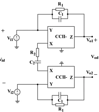
The proposed configuration can be used for realizing second order filters. By choosing,
1 1 1 1 1 ˆ sC R Y Y and 2 2 2 1 1 sC R Y
for the admittances shown in Fig. 3 a second order
all-pass/notch filter can be obtained as shown in Fig. 7.
The differential output voltage in this case is given by id o o od V C C R R s C R C R s C C R R s C R C C R C C s V V V 2 1 2 1 1 1 2 2 2 2 1 2 1 1 1 2 1 2 1 2 2 2 1 1 ) 1 1 ( 1 ) 1 2 ( (29)
By expressing the output V as given in (7) od
2 1 2 1 1 1 2 2 2 2 1 2 1 1 1 2 1 2 1 2 2 1 1 1 1 1 2 C C R R s ) C R C R ( s C C R R s ) C R C C R C C ( s Adm (30) and 0 cm A (31) are obtained. 3.2.1. All-Pass-Section
For realizing the second order all-pass filter the following condition must be satisfied:
1 1 2 2 1 1 2 1 2 1 2 1 1 1 2 C R C R C R C C R C C , (32)
which forces the following relation between resistor values
1 2 1 2 (1 )R C C R (33)
Then the filter has the phase response:
2 2 1 2 1 1 1 2 2 1 ) 1 1 ( arctan 2 ) ( C C R R C R C R (34)
As opposed to the first order realizations this circuit yields a phase shift from 0o to -360o and better pole frequency sensitivity. The pole frequency and the related sensitivities are:
2 1 2 1 2 1 C C R R fp (35)
2
/
1
p i p i f C f RS
S
for i=1,2.3.2.2. Notch Filter
Another advantage of the circuit shown in Fig. 7 is its tunability by adjusting the value of resistor R2 (via the bias current I0 in the BJT implementation) to obtain a notch filter. Using:
1 2 1 2 (2 )R C C R (36)
in the expression (30) for the gain yields:
2 1 2 1 1 1 2 2 2 2 1 2 1 2 1 1 1 1 C C R R s ) C R C R ( s C C R R s Adm (37)
As implied by (37) the notch frequency occurs at
2 1 2 1 2 1 C C R R fn
with same sensitivities.
4. TRACKING ERROR AND MISMATCH ANALYSIS
Taking into account the current conveyor non-idealities the terminal relations in (1) can be expressed as
IZ=IX VX=VY and IY=0 (36)
where =1-i and =1-v. Here i and v (i<<1 andv<<1) represent the current and voltage
tracking errors of the current conveyors, respectively. Reanalyzing the proposed configuration shown in Fig. 3 and expressing the output in the form given in (7) yield:
id ic o o od V Y Y Y Y Y Y V Y Y Y Y Y Y V V V 1 1 2 1 1 2 1 2 2 1 1 1 2 1 1 2 1 2 1 2 2 1 ˆ 2 ) ˆ )( ( 1 ˆ ) ˆ )( ( (37) 2 1 ( 1 2)( 2Zˆ1Y2 1Z1Y2 ) Adm (38) and ) ˆ )( ( 2 1 2Z1Y2 1Z1Y2 Acm (39)
where Z=1/Y. Note that:
i) Z1, Zˆ Y1, 2,being rational functions, the denominator in (38) therefore all pole frequencies are
independent of tracking errors and the notch frequency is independent of voltage tracking errors 1, 2.
ii) in this case the common-mode gain (Acm) of the configuration is not equal to zero. The
common-mode rejection ratio of the filter can be found theoretically as:
) ˆ )( ( 2 ) ˆ )( ( ˆ 2 log 20 log 20 2 1 1 2 1 2 1 2 2 1 1 2 1 2 2 1 1 1 10 10 Y Y Y Y Y Y Y Y Y Y A A CMRR cm dm (40)
which shows that the CMRR of the filter has a very high value because both of the parameters
1 and 2 are close to unity,
iii) for nominal values of all parameters Vod is related to Vid by:
Vod = (1 2Z1Y2) Vid (41)
In the sequel 1 2 1 will be assumed to simplify the analysis and not without justification since the designer must exercise special care to ensure the rejection of the common mode voltage at the output as expressed in (37).
Letting Zˆ1 Z1Z1 and Vod Vod for the disturbed output,
i i
idod
od V Z Y Z Z Y V
V 1 1 2(11)( 1 1) 2(1 2) (42) and using (41) equality (43) is obtained for the deviation in the output.
i i i
idod Z Z YV
V (1 2) 1 (1 2) 1 2
(43)
Neglecting second order terms and that |1 2Z1Y2| = 1, the expression for the relative error
then becomes : 2 1 1 1 2 1 ) ( Z Y Z Z V V i i od od (44)
To get a feeling of what equality (44) means leti1 i2 0, then
C j R Z V V od od / 1 2 1 which
decreases in the worst case to
2 1 R Z V V od od
as e.g. for R2=Rx1 + Rx2 = 1300(as is the
case for only C all-pass filter simulation with Io1 Io2 20A for CCCIIs),
1300 1 Z V V od od
5. SIMULATION RESULTS
All the circuits have been simulated using the SPICE simulation program to verify the theoretical analysis.
5.1. First Order RC All-Pass Filter Simulation
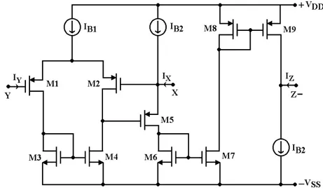
For the conveyor CCII- in the first order all-pass filter the schematic implementation shown in Fig. 8 [22] with a DC supply voltage 2.5V has been used.
Figure 8. CMOS implementation of the CCII-.
Transistors are simulated using 0.35m TSMC CMOS technology with parameters given in Table 1. and dimensions in Table 2. For the first order all-pass filter shown in Fig. 4 the element values are selected as: C=100pF and R1=R2=10k, IB1=200A, IB2=100A which result in a 90o
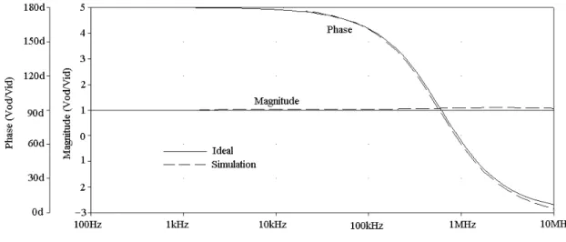
phase shift at fp=158.8 kHz and is very close to its ideal value (fp=159.1 kHz).
The magnitude and phase characteristics of the simulated circuit are shown in Fig. 9 from which it can be seen that the simulation results agree quite well with the theoretical analysis.
Table 1. 0.35m TSMC Model parameters of MOS transistors
.MODEL NM NMOS (LEVEL=3 TOX=7.9E-9 NSUB=1E17 GAMMA=0.5827871 PHI=0.7 VTO=0.5445549 + DELTA=0 UO=436.256147 ETA=0 THETA=0.1749684 KP=2.055786E-4 VMAX=8.309444E4
+ KAPPA=0.2574081 RSH=0.0559398 NFS=1E12 TPG=1 XJ=3E-7 LD=3.162278E-11 WD=7.046724E-8
+ CGDO=2.82E-10 CGSO=2.82E-10 CGBO=1E-10 CJ=1E-3 PB=0.9758533 MJ=0.3448504 CJSW=3.777852E-10 + MJSW=0.3508721)
.MODEL PM PMOS (LEVEL=3 TOX=7.9E-9 NSUB=1E17 GAMMA=0.4083894 PHI=0.7 VTO=-0.7140674 + DELTA=0 UO=212.2319801 ETA=9.999762E-4 THETA=0.2020774 KP=6.733755E-5 VMAX=1.181551E5 + KAPPA=1.5 RSH=30.0712458 NFS=1E12 TPG=-1 XJ=2E-7 LD=5.000001E-13 WD=1.249872E-7
+ CGDO=3.09E-10 CGSO=3.09E-10 CGBO=1E-10 CJ=1.419508E-3 PB=0.8152753 MJ=0.5 + CJSW=4.813504E-10 MJSW=0.5)
Table 2. Transistor dimensions of the CCII-. Transistor W [m] L [m]
M1, M2 24 0.35
M3, M4, M6, M7 10 1.5
M5, M8 M9 15 1.5
Figure 9. The magnitude and phase characteristics of the first order all-pass filter of Figure 4. 5.2 First order only C All-Pass Filter Simulation
The only C filter shown in Fig. 6 has been simulated using the CCCII- schematic implementation shown in Fig. 10 [21] with a DC supply voltage of 2.5 V.
Y X I +V 1 2 3 4 5 7 9 10 11 12 13 Q Q Q Q Q Q Q Q Q Q Q Q 8 Q O Q Q 6 14 15 16 17 Q Q CC EE -V Z I x y I z I I I I I 4 3 1 2 18 Q
Figure 10. Schematic implementation for the CCCII.
The PNP and the NPN transistors have been simulated using the parameters of the PR100N and NR100N bipolar transistors [23]; they are shown in Table 3.
Table 3. Model parameters of BJT’s NR100N and PR100N .MODEL NR100N NPN (IS=121E-018 BF=137.5 VAF=159.4 IKF=6.974E-3 ISE=36E-16 + NE=1.713 BR=0.7258 VAR=10.73 IKR=2.198E-3 RE=1 RB=524.6 RBM=25 RC=50 + CJE=0.214E-12 VJE=0.5 MJE=0.28 CJC=0.983E-13 VJC=0.5 MJC=0.3 XCJC=0.034 + CJS=0.913E-12 VJS=0.64 MJS=0.4 FC=0.5 TF=0.425E-9 TR=0.425E-8 EG=1.206 + XTB=1.538 XTI=2)
.MODEL PR100N PNP (IS=73.5E-018 BF=110 VAF=51.8 IKF=2.359E-3 ISE=25.1E-16 + NE=1.650 BR=0.4745 VAR=9.96 IKR=6.478E-3 RE=3 RB=327 RBM=24.55 RC=50 + CJE=0.180E-12 VJE=0.5 MJE=0.28 CJC=0.164E- 12 VJC=0.8 MJC=0.4 XCJC=0.037
+ CJS=1.03E-12 VJS=0.55 MJS=0.35 FC=0.5 TF=0.610E-9 TR=0.610E-8 EG=1.206 + XTB=1.866 XTI=1.7)
The element values are selected as: C=200pF, Io1=Io2=20A (Rx1=Rx2=650) which result in a
90o phase shift at fp=608 kHz and is very close to its ideal value (fp=612.1kHz). Magnitude and
phase characteristics of the simulated circuit are shown in Fig. 11 and the simulation results agree quite well with the theoretical analysis.
Figure 11. The magnitude and phase characteristics of the only C all-pass filter. 5.3 Second Order All-Pass Filter Simulation
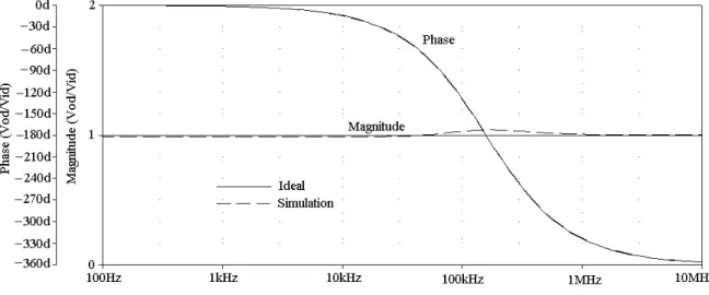
The second order all-pass circuit shown in Fig. 7, has been simulated with the schematic implementation shown in Fig. 8 and MOS model parameters and dimensions given in Table 1 and 2, respectively. The element values are selected as: C2=2C1=100pF and R1=2R2=20k,
IB1=200A, IB2=100A which result in a 180o phase shift at fp=160 kHz and is very close to its
ideal value (fp=159.1 kHz). Magnitude and phase characteristics of the simulated circuit are
Figure 12. The Magnitude and Phase characteristics of the second-order all-pass filter. 5.4 Notch Filter Simulation
Keeping the same element values as for second order all-pass filter but changing R2 to 30 k the
characteristic shown in Fig. 13 is obtained for the notch filter. The theoretical notch frequency being fn=91.8 kHz, the simulated notch frequency was found to be fn=90.2 kHz showing very
good agreement.
Figure 13. Magnitude characteristic of the notch filter.
6. EXPERIMENTAL RESULTS
The first and second order RC all-pass filters shown in Figs. 4 and 7 are constructed on National Instrument experimental board (Elvis) using AD844-type current conveyor (CCII+) IC of Analog Devices, 1% tolerance discrete resistors and polystyrene capacitors. The supply voltages are chosen as 5V. To implement a CCII- , two CCII+ are used as shown in Fig. 14.
Figure 14. Implementation of a CCII- using two CCII+.
The circuit of Fig. 4 is constructed with R1=R2=10k, C=10nF. The experimental result shows
that the input and output signals are in 90o phase difference at a pole frequency of 1.60 kHz as shown in Fig. 15.
Fig. 16 shows the experimental results for the circuit of Fig. 7 obtained with R1=2R2=20k,
C2=2C1= 10nF which results in a 180o phase difference between input and output signals at the
circuit pole frequency 1.60kHz.
Figure 15. Experimental results of the first order RC all-pass filter (vertical scale: 100mV/divider, horizontal scale: 200µs/divider, blue color: output; green color: input).
Figure 16. Experimental results of the second order all-pass filter (vertical scale: 100mV/divider, horizontal scale: 200µs/divider, blue color: output; green color: input).
7. CONCLUSION
In this paper a fully differential high CMRR general configuration for realizing first and second order all-pass and notch filters has been presented. The proposed configuration contains two CCII-s and three admittances. Two realizations for first order all-pass filter and one realization for second order all-pass filter have been given; it has been also shown that the second order filter can be tuned to behave like a notch filter. The pole frequency of the proposed filters and the notch frequency can be changed without disturbing the gain of the circuit. The non-ideality effects of current conveyors and element mismatches on the CMRR, voltage gains, pole and notch frequencies of the filters have been investigated and shown to be of negligible effect. The experimental and simulation results are given and shown to be in good agreement with theoretical analysis.
8. REFERENCES
[1] A. M. Soliman, “Inductorless realization of an all-pass transfer function using the current conveyor”. IEEE Transactions on Circuit Theory, CT-20, pp. 80-81, 1973.
[2] R. I. Salawu, “Realization of an all-pass transfer function using the second generation current conveyor”. Proceedings of the IEEE, 68, pp. 183-184. 1980.
[3] K. Pal, “Realisation of current conveyor all-pass network”. International Journal of Electronics, vol. 50 (2), pp. 165-168, 1981.
[4] K. Pal, “ Inductorless current conveyor allpass filter using grounded capacitors”., Electronics Letters, vol. 18 (1), pp. 47, 1982
[5] M. Higashimura, Y. Fukui, “Realization of all-pass networks using a current conveyor”, International Journal of Electronics, vol. 65 (2), pp. 249-250, 1988.
[6] M. Higashimura, Y. Fukui, “Realization of current mode all-pass networks using a current conveyor”, IEEE Trans. CAS, vol. 37 (5), pp. 660-661, 1990.
[7] C.M. Chang, “Current mode allpass/notch and bandpass filter using single CCII”. Electronics Letters, 27 (20), pp. 1812-1813, 1991.
[8] M. Higashimura, “Current-mode all-pass filter using FTFN with grounded capacitor”. Electronics Letters, 27 (13), pp. 1182-1183, 1991.
[9] A.M. Soliman “Generation of current conveyor based all-pass filters from op-amp based circuits”, IEEE Trans. CAS-II. vol.44 (4), pp. 324-330, 1997.
[10] A.M. Soliman, “New all-pass and notch filters using current conveyors”, Frequenz, vol 53 (3-4), pp. 84-86, 1999
[11] O. Cicekoglu, H. Kuntman, S. Berk, “All-pass filters using a single current conveyor”, International Journal of Electronics, vol. 86, (8): 947-955, 1999.
[12] S.J.G. Gift, “The application of all-pass filters in the design of multiphase sinusoidal systems”, Microelectronics Journal, vol. 31, pp. 9-13, 2000.
[13] A. Toker, S. Ozoguz, O. Cicekoglu, C. Acar, “Current-Mode all-pass filters using current differencing buffered amplifier and a new high-Q bandpass filter configuration”, IEEE Trans. on CAS-II. vol. 47, (9), pp. 949-954, 2000.
[14] U. Cam, O. Cicekoglu, M. Gulsoy, H. Kuntman, “New voltage and current mode first-order all-pass filters using single FTFN”, Frequenz, vol. 54, (7-8), pp. 177-179, 2000.
[15] I. Khan, S. Maheshwari, “Simple first order all-pass section using a single CCII”, International Journal of Electronics, vol. 87 (3), pp. 303-306, 2000.
[16] S. Maheshwari, I. Khan, “Novel first order all-pass sections using a single CCIII”, International Journal of Electronics, vol. 88 (7), pp. 773-778, 2001.
[17] S. Minaei, O. Cicekoglu, “A new resistorless electronically tunable voltage-mode first-order phase equalizer”, Proceedings of the 2003 IEEE International Symposium on Circuit and Systems (ISCAS 2003), 25-28 May 2003, Bangkok, Thailand, Vol I., pp. 465-468. [18] S. Minaei, “A new high performance CMOS third generation current conveyor(CCIII) and
[19] P.E. Allen, D.R. Holberg, “CMOS analog circuit design”, Oxford University Press, 2nd Edition, New York 2002.
[20] B. Wilson, “Recent developments in current conveyor and current mode circuits”, IEE proceedings Part G. vol. 132, pp. 63-77, 1990.
[21] A. Fabre, O. Saaid, F. Wiest, C. Boucheron, “ High frequency applications based on a new current controlled conveyor”, IEEE Trans. on CAS-I. vol. 43 (2), pp. 82-91, 1996.
[22] H.-Y. Wang, C.-T. Lee,“Versatile insensitive current-mode universal biquad implementation using current conveyors”, IEEE Trans. on CAS-II. vol. 48 (4), pp. 409-413, 2001.
[23] D.R. Frey, “Log-domain filtering: an approach to current-mode filtering”, IEE ProceedingsG, Circuits, Devices and Systems, 140, (6) pp. 406416, 1993.
![Table 2. Transistor dimensions of the CCII-. Transistor W [ m] L [ m]](https://thumb-eu.123doks.com/thumbv2/9libnet/4061998.57676/14.892.132.783.100.537/table-transistor-dimensions-ccii-transistor-w-m-l.webp)