200 IEEE TRANSACTIONS ON CIRCUITS AND SYSTEMS-11. ANALOG AND DIGITAL SIGNAL PROCESSING, VOL. 40, NO. 3. M A R C H 1993
Transactions Briefs
Analog CMOS Implementation
of Cellular Neural Networks
Izzet Adil Baktir and Mehmet Ali TanAbsfract- The analog CMOS circuit realization of cellular neural networks with transconductance elements is presented. This realization can he easily adapted to various types of applications in image processing just by choosing the appropriate transconductance parameters according to the predetermined coefficients. The effectiveness of the designed circuits for connected component detection is shown by HSPICE simulations. For “fixed function” cellular neural network circuits the number of transistors are reduced further by using multi-input transconductance elements.
I. INTRODUCTION
The term artijcial neural network (ANN) has come to mean any computing architecture that consists of massively parallel in- terconnections of simple neural processors [ I ] , [2]. Artificial neural networks try to mimic, at least partially, the structure and functions
of the brain and the nervous system. The implementation artificial neural networks in VLSI takes advantage of the inherent parallelism to yield fast solutions [3]. In the VLSI implementation of neural networks, analog VLSI techniques are preferable because they lead to more compact and real-time realizations [4]-[7].
The cellular neural network (CNN) as proposed by Chua and Yang, is a special type of analog nonlinear processor array [8], [9]. Due to their continuous-time dynamics and parallel processing features, analog CNN circuits are very effective in real time image processing applications such as noise removal, edge detection and feature extraction [8]. The regularity, the parallelism and the local connectivity found in CNN circuit architecture make it suitable for VLSI implementations.
Motivated by the above facts we have implemented the CNN structure using analog CMOS circuits. One of our major goals is the design simplicity. To achieve this goal, the design is reduced to the design of few type of CMOS transconductance elements [ 101. One can easily adapt this realization to various types of applications by just choosing the appropriate transconductance parameters according to the predetermined coupling coefficients between the neighboring cells. The coefficients may be either chosen according to a computer simulation or chosen based on the prominent kernels for image processing [ 111. Another important motivation for using CMOS transconductance elements in the requirement of adaptability. In order to acheive programmable coupling coefficients, the transconductance parameters are adjustable with extemal voltage sources. In the implementation of “fixed function” CNN’s that performs one or a
related set of processing function using fixed coefficients, the number of transistors is reduced further by merging appropriate transistors in the multi-input transconductance subcircuit as explained in Section 111.
Manuscript received July 8, 1992; revised October 20, 1992.
The authors are with the Department of Electrical and Electronics Engi- IEEE Log Number 9208101.
neering, Bilkent University, 06533 Bilkent, Ankara, Turkey.
VDD
I
I
vss
(b)
of CMOS transconductance element.
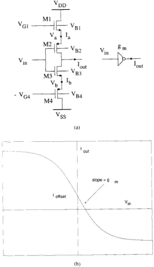
Fig. 1. (a) The transistor schematic and (b) the input4utput characteristic
11. ANALOG CMOS REALIZATION OF THE CELL CIRCUIT Because of its simplicity, the CMOS transconductance element is chosen as the basic building block for the integrated realization o f the CNN cell circuit [12]. The linear CMOS transconductance element (voltage-to-current transducer) resembles in most respects that of the CMOS inverter but without the matching problems between PMOS
and NMOS transistors and with the additional advantage of tunability [ 121. The transistor schematic and the input-output characteristic of this four-transistor transconductance element is shown in Fig. 1.
It can be easily proven that when all transistors operate in their saturation region [12], the output current I,,t = I , - Ib equals
( 1 )
I,,”, = -.ym1;,,
+
Lff
where the abbreviationsgni =2k,ff[[I.i;1
+
1;;4 - ( l i n l+
[ I . i , G i+
I l i , 2 l+
l l i I , . 4 l ) ] (2) 1057-7130/93$03.00 0 1993 IEEEbias
ukl
ykl
s;y
Fig. 2. The cell circuit realimtion with CMOS transducers.
( 3 )
are introduced for the transconductance parameter and the offset current, respectively.
Although the offset current I,,E is not equal to zero due to the body effect, it can be easily elminated by an appropriate setting of I
Ht
in an n-well process andI h I
in a p-well process [ 121.2.1. Realization of a Cell with CMOS Transconductances
The circuit diagram of the integrated circuit reahation of one CNN cell with CMOS transconductance element is shown in Fig. 2. It consists of the summation node o , ~ . where all the input currents and the bias current are summed, the state and output resistors, the input and output voltage-controlled current sources and a block realizing the sigmoid function.
The main problem in VLSI circuits is the implementation of the resistors that are not commonly used in standard CMOS technology. They usually occupy a large chip area which makes it impossible to implement networks with huge number of resistors. In order to eliminate this problem, we have implemented the cell circuit resistors
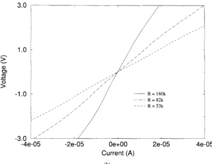
R, and R,. by simply connecting the input of the transconductance to its output as shown in Fig. 3(a). The desired resistance values are achieved by choosing the gate area width-to-length ratio (W/L) appropriately after having set I>;, = I 7 ~ ~ ~ > = S V and -12; I = 1i.s = -5 V. Adjustable resistance can also be easily achieved by varying I;;% and I;;, externally. SPICE simulation results for different resistance values are shown in Fig. 3(b).
The sigmoid type nonlinear transfer characteristic needed at the output of the cell is performed with two transconductance elements. The second transconductance element whose input is connected to
V
I
+TI
+T
I
(a)
Fig. 3. (a) The circuit diagram.
v ( r
= l / g
-1
its output, acts like the resistor R , and the output voltage v Y drives individual current sources whose outputs are coupled to the neighbors. Since input voltages o u and the output voltages I ' ~ are bounded by
*
1 V, the input control and the output feedback voltage-controlled current sources are obtained by using the transconductance elementsy L . g ( i . , j : A , . [ ) and , q r < ( ( i . , j : k . / ) in their linear region.
The desired coupling coefficient can be easily achieved by simply choosing the appropriate transconductance parameters. In order to perform one or a related set of processing functions using fixed co- efficients, the transconductance parameter variation can be achieved by choosing the gate area W/L appropriately after having set I >;I =
T - f ~ r , = SV and -\;;I = 1 - 5 5 = - 3 V. The negative (inhibitory) coupling coefficients can be obtained by inverting the positive (exci- tatory) input with a cascaded transconductance element pair as shown in Fig. 4.
The analog input data (initial state voltages and input voltages) and the output data (final output voltages) can be multiplexed row by row using two switches in each cell circuit [ 131. Also, the synchronization of the transient continuous-time operation can be achieved by a start control signal [ 131.
In the designed circuit, the stability requirement of Chua [8]: 1
A ( i . j : i , j )
>
-R ,
is achieved by choosing
2.2. Programmable Coupling Coeflcients
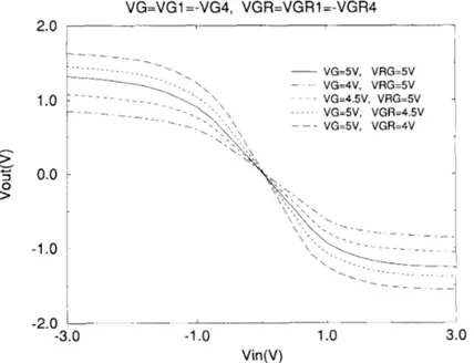
The requirement of adaptability is difficult to achieve in most neural network VLSI implementations [ 141, [ 151. In the realization of the CNN structure with CMOS transconductance elements, we can achieve a programmable implementation by varying the transconduc- tance parameters with external voltage sources connected to the gate voltages IC1 and l i ; 1 of each cell defined in (2). HSPICE simulation results of the transconductance parameter variation for different gate voltages are shown in Fig. 5 .
Nevertheless, one of the major concerns in VLSI programmable implementations of CNN is the wiring needed for changing the
A =
~
202 IEEE TRANSACTIONS ON CIRCUITS AND SYSTEMS-11: ANALOG AND DIGITAL SIGNAL PROCESSING, VOL. 40, NO. 3, MARCH 1993
3.0
1
.o
hL
a, 0 (U 0>
c-
-1
.o
-3.0
/ / / /,
,
/
-4e-05
-2e-05
Oe+00
2e-05
Current
(A)
4e-05
Fig. 3. (b) The characteristic of a CMOS resistor for different resistance values.
Fig. 4. Inhibitory coupling coefficients with CMOS transconductance elements.
template coefficients of each cell. Since all the cells of a CNN have the same coupling coefficients g r u ( i . j : k . 1 ) and g z < , ( i . j : k . 1 ) . the wiring problem can be largely eliminated by controlling the transconductance parameter variation of all cells with the same set of external gate voltages.
and
111. REDUCED H A R D W A R E
In order to decrease the number of transistors in the realiza- tion of “fixed function” CNN structure, we propose a multi-input transconductance element which is shown in Fig. 6. The multi-input transconductance element is similar to vi transconductance element proposed by Park et al., except that upper NMOS and lower PMOS
transistors are common [ 121.
In dc analysis of this new twinput voltage-controlled current source, assuming matching between NMOS transistor 311 and PMOS transistor ,212 and using the standard square-law model for MOS transistors in their saturation region, the current I,,,,, can be derived as
I I
‘G4
‘GR4
Fig. 5. (a) The circuit diagram.
I,?
U ’ , = 1 alld U ’ ,
> 0
(9)t = 1
where k,,, and AV, are the i t 1 1 NMOS and j t h PMOS transistor parameters, W , ’ S are the ratios between transistors and rrc is the number of input voltages.
The inhibitory coupling coefficients can be obtained by inverting the positive (excitatory) input with a cascaded transconductance element pair shown in Fig. 4. It can be easily shown that the maximum of the A term defined in (7) is less then 0.015, that is,
The derivations of the output current and maximum percentage error (4)
are as shown in (5)-(7) on the t ” m of the The conditions that should be satisfied in the derivative of (4) are
are given in Appendix A .
Since the maximum error is less the IS%, this multi-input VCCS can also be used in the implementation of fixed function CNN
SPICE simulation results of three-input vCCs
I,,,t = ! l c f f ( U ’ 1 1 i
+
11’21;+
l L ’ 3 l i ) +I”ff wherem ~ .
previous page. and
VG=VGl =-VG4, VGR=VGRl =-VGR4
2.0
11
.o
0.0
-1
.o
1-2.0
'
-3.0
-1
.o
1
.o
3.0
Vin(V)
Fig. 5. (b) The simulation results of the tranFconductance parameter variation for different gate voltages.
M 2m+2
Fig. 6. II-input voltage-controlled current source.
IV. SIMULATION RESULTS FOR
CONNECTED COMPONENT DETECTOR
When the CMOS implementations described above are being used in an image processing application, the images are presented to the network as a set of initial input voltages to the state capacitors. The basic function of a CNN for image processing is to map an input image into a corresponding output image which are restricted with fl V as pixel values [9], [ 161, [17]. How to choose the circuit parameters to achieve a desired image transformation is currently still an active research problem [18], [19].
In handwritten character recognition and many other feature ex- traction processes, the CNN circuits can be used as a connected component detector which detects the number of connected com- ponents of a vector in
{+I,
-1)" 1131, 1201.To achieve the CNN cloning template for connected component detector given in [13], the parameters of our circuit are chosen as
follows: -4 = [.qr(i..j: i - 1. j ) q s ( i , j : i, j ) yr.(;. j : i
+
1. j ) ] = . y z [ l 2 - 11 B = 0 .rim,
= 0 R , = 1 0 0 K R C =4pF.With the above circuit parameters, a 1 x 1 2 analog CMOS CNN circuit is simulated using the circuit simulator HSPICE. The set of
initial conditions and the corresponding steady state values for the state voltages u , . , ( t ) for 1
5
i5
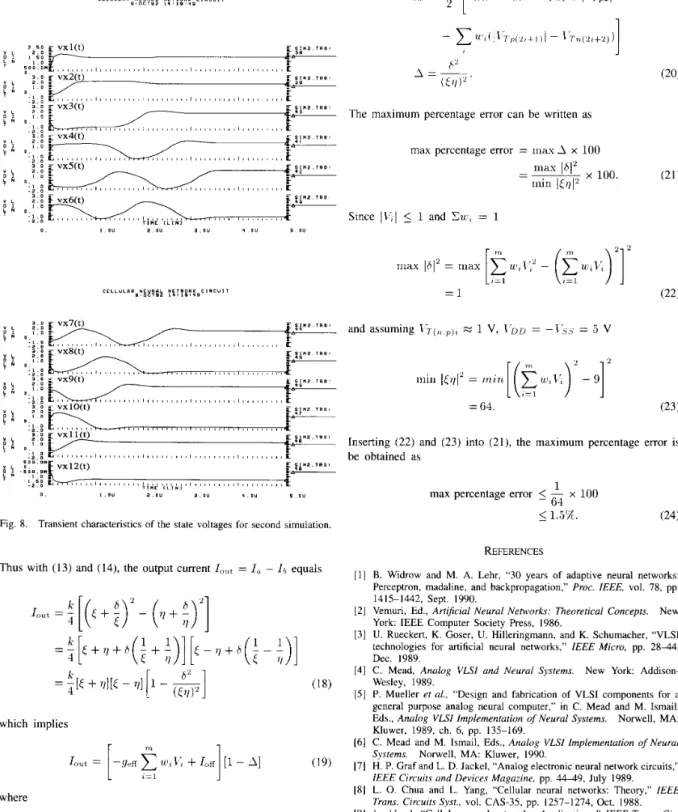
1 2 is given in Table I.To see the dynamic behavior of the circuit in more detail, the output transient characteristics of the state voltages are shown in Fig. 8. These transient characteristics show that the cell outputs reach their appropriate steady state values depending on both their neighbor cells and initial condition in less than 3.5 / i s .
V. CONCLUSION
A new analog CMOS circuit implementation of a CNN has been presented. The design of CNN circuits is reduced to a transcon- ductance element and it can be easily adapted to various types of applications by just tuning the appropriate transconductance elements according to the predetermined coupling coefficients between the neighboring cells in connected detector example.
The realization of CNN with CMOS transconductance elements can be either programmable or fixed function. In order to reduce the wiring problems in programmable CNN circuits, the desired cou- pling coefficients can be achieved by changing the transconductance parameters of each cell circuit with the same set of external voltage sources.
By using modified multi-input transconductance elements, the total number of transistors required for a cell circuit of connected component detector i s reduced to 28. Since the number of transistors
204 IEEE TRANSACTIONS ON CIRCUITS AND SYSTEMS-II: ANALOG AND DIGITAL SIGNAL PROCESSING, VOL. 40, NO. 3, MARCH 1993
State Initial Final
1
.o
" Z 2 Ur3 v,q t,z5 L:,6 e's7 ('LU ('19 1 k 1 0 "z11 rr12
1.0 -1.0 -1.0 1.0 -1.0 -1.0 -1.0 -1.0 1.0 -1.0 -1.0 1.0 1.4 1.4 1.4 1.4 1.4 2.0 -1.4 1.4 -1.4 1.4 -1.4 1.4 0.5 State Initial Final h
L
c -J 0.0 0>
v x l vs2 t ' X 3 U,* l ' x 5 I S x 6 U , i Us8 rz9 '210 " r l l C x l Z 1.0 -1.0 -1.0 1.0 -1.0 1.0 -1.0 -1.0 1.0 1.o
-1.0 -1.0 1.4 1.4 1.4 1.4 2.0 -1.4 1.4 -1.4 1.4 -1.4 1.4 -1.4 -0.5 State Initial Final -1.o
z',1 " X 2 "Z3 I ' z l i'& j I ' x 6 L's i 1'18 l ' L 9 [',lo 21x11 ",lZ -1.0 -1.0 -1.0 1.0 1.o
-1.0 -1.0 1.0 1.o
-1.0 -1.0 -1.0 1.4 1.4 1.4 1.4 2.0 -1.4 1.4 -1.4 1.4 -1.4 1.4 -1.4VOut=
wl
* V 1 + ~ 2 * V 2 + ~ 3 * V 3
-2.0
0.0
Vin(V)
2.0
TABLE IHSPICE SIMULATION RESULTS FOR THREE DIFFERENT IINITIAL STATES
needed i s less than the previous approaches given in [ 131 and [ 141, with the proposed approach it is possible to increase the number of cells in the VLSI implementations of CNN's.
in Fig. 6, are easily derived as
VI. APPENDIX A
For the m-input transconductance element shown in Fig. 6, let
and
m
c w t = 1 and w,
>
0% = I
where b,, and IC,, are the ith NMOS and j t h PMOS transistor parameters, w , ' s are the ratios between transistors and rri is the number of input voltages.
In dc analysis, using the standard square-law model for MOS transistors in their saturation region, the currents I , and I b , defined
and
where
and
E =
- ~ 4 \ - T r l d 2 j + L i - T ? n ( L z f 2 ) )
I
h2
( € V P
'A = -
The maximum percentage error can be written as
max percentage error = niax A x 100
0 . 1 . 0 " 2 . 0 " 3 . 0 " 4 . 0 " 5 . 0 "
Fig. 8. Transient characteristics of the state voltages for second simulation.
Thus with (13) and (141, the output current Iout = I , - Ib equals
which implies
where
Inserting (22) and (23) into (21), the maximum percentage error is be obtained as
1
64
max percentage error
5
- x 1005
1.5%REFERENCES
[I] B. Widrow and M. A. Lehr, "30 years of adaptive neural networks: Perceptron, madaline, and backpropagation," Proc. IEEE, vol. 78, pp. 1415-1442, Sept. 1990.
121 Vemuri, Ed., ArtiJicial Neural Networks: Theoretical Concepts. New York: IEEE Computer Society Press, 1986.
[3] U. Rueckert, K. Goser, U. Hilleringmann, and K. Schumacher, "VLSI technologies for artificial neural networks," IEEE Micro, pp. 2 8 4 , Dec. 1989.
[4] C. Mead, Analog VLSI and Neural Systems. New York: Addison- Wesley, 1989.
[SI P. Mueller et al., "Design and fabrication of VLSI components for a general purpose analog neural computer," in C. Mead and M. Ismail, Eds., Analog VLSI Implementation of Neural Systems. Norwell, MA: Kluwer, 1989, ch. 6, pp. 135-169.
[6] C. Mead and M. Ismail, Eds., Analog VLSI Implementation of Neural Systems. Norwell, MA: Kluwer, 1990.
171 H. P. Graf and L. D. Jackel, "Analog electronic neural network circuits,"
IEEE Circuits and Devices Magazine, pp. 44-49, July 1989. 181 L. 0. Chua and L. Yang, "Cellular neural networks: Theory," IEEE
Trans. Circuits Sysr., vol. CAS-35, pp. 1257-1274, Oct. 1988. 191 (-1 (-1, "Cellular neural networks: Applications," IEEE Trans. Cir-
[IO] M. A. Tan, "Synthesis of artificial neural networks by transconductors
c u i t ~ Syst., vol. CAS-35, pp. 1275-1290, Oct. 1988.
only," Analog Integrated Circuits and Signal Processing, vol. 1, pp. 339-35 I , 1991.
[ 1 I ] L. 0. Chua and P. Thiran, "An analytical method for designing simple cellular neural networks," IEEE Trans. Circuits Syst., vol. 38, pp.
lEEE TRANSACTIONS ON CIRCUITS AND SYSTEMS-11. ANALOG AND DIGITAL SIGNAL PROCESSING. VOL. 40, NO. 3, M A R C H 1993
C. S . Park and R. Schaumann, “A high frequency CMOS linear transconductance element,” IEEE Trans. Circuits Syst., vol. 33, pp. 1131-1138, Nov. 1986.
J. M. Cruz and L. 0. Chua, “A CNN chip for connected component detection,” IEEE Trans. Circuits Syst., vol. 38, pp. 812-817, July 1991. L. Yang, 0. Chua, and K. R. Krieg, “VLSI implementation of cellular neural networks,” in Proc. Int. Symp. on Circuits and Systrms 1990, pp. 2425-2421, May 1990.
M. Verleysen and P. G. A. Jespers, “An analog implementation of Hopfield’s neural network,” IEEE Micro, pp. 46-55, Dec. 1989. T. Matsumoto, T. Yokohama, H. Suzuki, R. Furukawa, A. Oshimoto, T. Shimmi, Y. Matsushita, T. Seo, and L. 0. Chua, “Several image processing examples by cellular neural networks,” in Proc. Int. Workshop on Cellular Neural Networks and Their Applications 1990, pp. lOG106, Dec. 1990.
G. Serker, “Small object counting with cellular neural networks,” in
Proc. Int. Workshop on Cellular Neural Networhs and Their Applications 1990, pp. 139-148, Dec. 1990.
F. Zou, S. Schwarz, and J . A. Nossek, “Cellular neural network design using a learning algorithm,” in Proc. Int. Workshop on Cellular Neural
Networks and Their Applications 1990. pp. 73-8 1, Dec. 1990. K. Slot, “Determination of cellular neural network parameters for feature detection of two dimensional images,” in Proc. Int. Workshop
on Cellular Neural Networks and Their Applications 1990, pp. 82-91, Dec. 1990.
T. Matsumoto, L. 0. Chua, and H. Suzuki, “CNN cloning template: Connected component detector,” IEEE Trans. Circuils Syst., vol. CAS- 37, pp. 633-635, May 1990.
CMOS Implementation of an Analogically
Programmable Cellular Neural Network
G. F. Dalla Betta, S. Graffi, Zs. M. Kovacs, and G. MasettiAbsfract- The criteria to design the basic building blocks of an analogically programmable cellular neural network (CNN) in a 1.5-pm CMOS technology are reported. The simulated electrical performances of a 10 x 10 CMOS CNN, constituted of about SO00 MOS transistors, are presented and discussed. Finally, it is shown that the designed CNN can be successfully used to perform such useful functions as noise removal, edge detection, hole filling, shadow detection, and connected component recognition.
I. INTRODUCTION
In recent years, a great deal of research work has been done on artificial neural networks, as they can potentially be used for several practical applications such as speech and image recognition, whereas normal processors require a considerable amount of processing time. In particular, neural digital systems. either in parallel or serial form, neural analog electronic networks and neural optical systems have been suggested [I], [2].
Very recently, a new and altemative approach to the classic artificial neural network topologies, called cellular neural networks (CNN’s), was introduced by Leon Chua et al. 131, 141. Immediately after their introduction, CNN’s raised great interest as an alternative to conventional computers for image processing and pattern recognition
[51-[81, [101-[ 181.
Manuscript received July 24, 1992; revised November 6, 1992. The authors are with the Department of Electronics, University of Bologna, IEEE Log Number 9208 102.
40136 Bologna, Italy.
CNN’s exhibit several interesting features and properties; among these
a. b.
C.
the more important are:
each cell (or processing unit) is locally connected only to its neighbors:
the processed signals are analog in nature and the continuous- time operation allows the computational speed to depend only on the time-constant of the underlying dynamic system; the architecture of both the processing unit and of the inter- connection elements between cells is very simple and space invariant; this renders the CNN’s particularly suited for an implementation in a VLSI technology, like CMOS.
Up to now, only a few proposals of practical CNN implementations have been published [ 5 ] - [ 8 ] . In particular, in 161 a CMOS design in a current-mode approach of a 10 x 10 simple low-pass filter for noise removal has been proposed, while in [7] a 6 x 6 connected-component detector (CCD) has been designed, fabricated, and experimentally tested. As a matter of fact, the work of [7] represents the only CNN chip fabricated up to now. All of these designs refer to given established applications for which the weights of the interconnections between elementary cells (the so-called template weights) are fixed. However, in practice, the possibility to manage a neural network to be used for different applications in different time periods of the signal processing procedure is particularly interesting, as one can use the same part of the chip to perform several circuit functions. In this context, a CMOS approach for the design of a reconfigurable cellular network in which the template coefficients can be digitally varied was proposed in [ 5 ] . Unfortunately, however, even if this approach i s very interesting from a circuit point of view, the control circuitry required to digitally select the template coefficients values leads to a very complex final architecture.
In this work we will present the design, in a 1.5-pm CMOS technology, of an analogically programmable CNN architecture with low-power dissipation which can be adopted for several applications in image processing. Additionally, the analogically programming feature can also be used to test the robustness of CNN performances against undesired variations in the values of the template Coefficients. In Section 2.1 the design of the elementary processing unit and of the linear voltage-dependent current sources that implement the feedforward template coefficients is presented. Section 2.2 is devoted to the design of the CMOS multiplier which enables to analogically program the ‘‘lateral’’ template coefficients of the feedback operator. Section 2.3 briefly discusses the differences between the ideal model and the CMOS implementation. Section I11 reports the electrical performances of a 10 x 10 CMOS CNN, constituted of about 8000
MOS transistors and fully simulated at the device level, which can simply be programmed by varying an external control voltage. By doing so, the designed CNN can perform such useful functions as noise removal, edge detection, hole filling, shadow detection and connected component recognition. Finally, some conclusions are drawn in Section IV.
11. DESIGN
2.
I
Cell Core and Control OperatorThe basic building blocks of the CNN have been developed with reference to a well-assessed 1.5-pm n-well CMOS technology with an oxide thickness of 250A. A circuit supply voltage of k 5 V was considered.