Journal of Sustainable Development of Energy, Water and Environment Systems
http://www.sdewes.org/jsdewes
Year 2019, Volume 7, Issue 2, pp 253-260
253
Journal of Sustainable Development of Energy, Water and Environment Systems
http://www.sdewes.org/jsdewes
An Energy Efficient Way to Produce Zinc-Based Semiconductor Thin
Films via Chemical Bath Deposition Technique
Sinan Temel*1, Fatma Ö. Gökmen2, Elif Yaman3
1Central Research Laboratory, Bilecik Seyh Edebali University, 11230 Gülümbe Köyü/Bilecik, Turkey
e-mail: [email protected]
2Central Research Laboratory, Bilecik Seyh Edebali University, 11230 Gülümbe Köyü/Bilecik, Turkey
e-mail: [email protected]
3Central Research Laboratory, Bilecik Seyh Edebali University, 11230 Gülümbe Köyü/Bilecik, Turkey
e-mail: [email protected]
Cite as: Temel, S., Gökmen, F. O., Yaman, E., An Energy Efficient Way to Produce Zinc-Based Semiconductor Thin Films via Chemical Bath Deposition Technique, J. sustain. dev. energy water environ. syst., 7(2), pp 253-260, 2019,
DOI: https://doi.org/10.13044/j.sdewes.d6.0239
ABSTRACT
In this study, zinc oxide, zinc sulfide and zinc selenide semiconductor thin films were produced by Chemical Bath Deposition technique with and without annealing. The structural, surface and optical properties of the obtained thin films were determined to specify effect of annealing on thin film properties. Characterization results indicated that, the produced zinc-based thin films have polycrystalline nature. Both zinc sulfide and zinc selenide thin films have cubic and zinc oxide thin films have hexagonal structure. The surface morphologies of all thin films are homogeneous and compact. The optical band gap values of the obtained thin films are close to the band gap of zinc-based semiconductors. The annealing processes neither improved the crystal structures nor altered the band gap values of zinc-based thin films. Agreeable to characterization results, production of zinc-based thin films via chemical bath deposition technique without annealing is facile, economic and energy efficient so can be used for many thin film applications.
KEYWORDS
Solar cells, Thin films, Chemical bath deposition, Semiconductors.
INTRODUCTION
Energy demand which is constantly increasing due to technological development is currently supplied by traditional fossil fuels such as coal, natural gas, petroleum products, etc. [1]. Fossil fuels have some disadvantages: they are thermally inefficient when converted to final product (a); it causes environmental and health problems (b) and the most important point is the fossil fuel reserves in the world is limited (c). Vagueness of the fossil fuel prices in the future is also another important drawback about use of fossil fuels [2]. Evaluation of renewable energy sources is the key parameter to overcome energy crisis [3]. Renewable and clean energy resources can be classified as wind, biomass, hydro and solar energy.
In semiconductor materials, zinc-based (zinc oxide, zinc sulphide and zinc selenide) which consist of II and VI group elements of the periodic table are significant elements to use in optical device technology [4]. Interest in II-VI materials stems from their wide band gap [5]. These materials are commonly used in applications of optoelectronic devices such as solar cells [6]. The advantages of zinc-based materials in comparison to other II-VI elements are that it is non-toxic, readily available and eco-friendly [7]. They can be obtained with high purity from cheap raw materials. Having wide band gap, high electron mobility and strong room-temperature luminescence are unique properties of Zinc oxide (ZnO) [8]. Because of these superior properties, ZnO is frequently used in the application of solar cells [9]. ZnO is also a promotive material for electronic, optoelectronic, information technology device and gas sensor applications due to its good electrical and optical properties [10]. Zinc sulphide (ZnS) is a wide band gap and direct transition semiconductor [11]. Because of its wide bandgap, ZnS has significant importance in light emitting diodes, cathode-ray tubes, thin film electroluminescence and window layers in photovoltaic cells application [12]. Zinc selenide (ZnSe) is another important II-VI group semiconductor material having a wide direct band gap [13]. It has an extensive application area in thin film devices, such as photoluminescent and electroluminescent devices and as an n-type window layer for thin film heterojunction solar cells [14].
Zinc-based thin films can be produced as a polycrystalline layer by conventional methods like as electron beam evaporation, Radio Frequency (RF) sputtering, pulsed laser deposition, ultrasonic spray pyrolysis, sol-gel method and chemical bath deposition technique [15]. These conventional techniques require high temperature annealing process to obtain high crystallinity. High temperature annealing process causes high energy consumption. In the method used in this work, there is no need to anneal as in other thin film deposition techniques. This provides energy savings.
In this work, zinc-based thin films have been synthesized on glass substrates, by Chemical Bath Deposition (CBD) technique and the structural, morphological and optical properties of the films have been investigated.
MATERIALS AND METHOD
Deposition technique and deposition process were given below in this section.
Chemical Bath Deposition technique
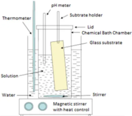
CBD is an easy method for production of thin films. This method is performed in a batch reactor, needs only a substrate to be immersed in a solution of aqueous precursors such as metal salts, complexing agents, and pH buffers. Highlights of CBD include cost-efficient, operation at atmospheric pressure, and scalability to large surface substrates [16]. In Figure 1, the schematic presentation of chemical bath deposition technique is shown.
Cleaning process of substrates
In this study, glass slides were used as substrate to deposit semiconductor thin films. Glass substrates were immersed in acetone and methanol for 5 minutes in ultrasonic bath respectively, then cleaned with distilled water and dried at 25 °C.
Preparation of zinc oxide thin films
0.1M Zinc nitrate hexahydrate [Zn(NO3)2.6H2O] (Sigma Aldrich) solution was
prepared in distilled water of 100 ml. The solution was stirred with a magnetic stirrer for 15 minutes. Then, pH of the solution was arranged to 10 by dropping ammonia solution (28% v/v) (Merck). After the bath was prepared, substrates were immersed in the solution. The solution with immersed substrate was mixed with temperature-controlled magnetic stirrer for 30 min at 85 °C. Prepared thin films were cleaned with distilled water and dried at 25 °C.
Preparation of zinc sulfide thin films
Zinc acetate dihydrate [Zn(CH3COO)2.2H2O], Tri-sodium citrate (Na3C6H5O7.2H2O)
and Tiourea (N2SCH4) from Sigma Aldrich were used synthesized ZnS films by CBD
technique. 0.15M Zn(CH3COO)2.2H2O, 0.5M Na3C6H5O7.2H2O and 1M N2SCH4
solutions were prepared and then blended. pH value of the final solution was fixed at 10, by dropping 28% aqueous ammonia solution. The two glass substrates were submerged in the prepared bath. The bath temperature was set at 80 °C for 90 minutes. Prepared films were cleaned with distilled water and dried at 25 °C.
Preparation of zinc selenide thin films
Zinc sulphate heptahydrate (ZnSO4.7H2O) and Selenourea [SeC(NH2)2] from Sigma
Aldrich were used to synthesize ZnSe thin films by CBD method, as well as Hydrazine hydrate (N2H5OH) from Merck as a stabilizer. Firstly, 0.5M ZnSO4.7H2O,
0.4M SeC(NH2)2 and 0.5M N2H5OH solutions were prepared in equal volumes.
28% aqueous ammonia solution was used to fix the pH of final solution to 10. Glass substrates were submerged in the bath. The bath temperature was set at 80 °C for 90 minutes. Prepared films were cleaned with distilled water and dried at 25 °C.
The structural, surface and optical properties of the obtained thin films characterized by applying X-Ray Diffraction (XRD), Field Emission Scanning Electron Microscopy (FESEM) and Ultra-Violet Visible (UV-Vis). Spectroscopy measurements, respectively.
RESULTS AND DISCUSSION
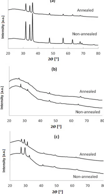
The crystal structure of the semiconductor thin films was investigated by XRD measurements which were performed by Panalytical Empyrean X-ray diffractometer using CuKα (λ = 1.5405 Ȧ) radiation in the 2θ range 20°-80° with a scanning speed of
2 °/min. The diffractometer reflection of the films was taken at the room temperature. An X-ray tube operated at 45 kV and 40 mA. According to XRD results, all produced zinc-based thin films have polycrystalline nature. The XRD diffraction pattern of the ZnO has matched completely with that of the hexagonal structured ZnO (ICDD: 98-003-1052), ZnS has matched with that of the cubic structured ZnS (ICDD: 98-004-2798) and ZnSe has matched with that of the cubic structured ZnSe (ICDD: 98-004-1983). In Figure 2, XRD spectra of zinc-based semiconductor thin films have been given comparatively.
As seen from the XRD results, the peak intensities of non-annealed zinc-based thin films are greater than the peak intensities of thin films annealed at 400 °C. For both non-annealed and annealed thin films’ Full Width at Half Maximum (FWHM) values and the grain size values calculated with Scherer’s formula are approximately the same.
The calculated average grain size value for both films is about 30 nm for ZnO, 23 nm for ZnS and 28 nm for ZnSe. According to these results, it seems that the annealing process does not have a healing effect on crystal structures of zinc-based thin films.
Figure 2. XRD spectra of: ZnO (a); ZnS (b) and ZnSe (c) thin films
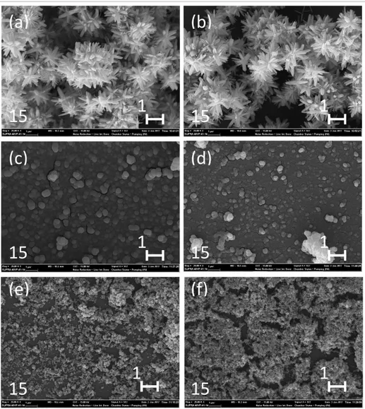
Morphological properties of the films were determined by FESEM (Zeiss Supra 40VP). In Figure 3, FESEM pictures of zinc-based thin films are presented. When the images of ZnO (Figure 3a and Figure 3b) thin films are investigated, it is seen that the morphological structure is formed consistently and detached from each other by nanorods. It is also examined that the nanorods integrate to form a flower-like structure. In the ZnS (Figure 3c and Figure 3d) pictures, it is seen that the film surface is constituted by almost homogeneously distributed nanostructured particles. It is also shown that there are no aggregations and there are no vacancies on the surface, so that the nano-particles are kept together better. In the ZnSe (Figure 3e and Figure 3f) images, it is demonstrated that the surface of the film is occurred from small accumulations and nano-particles in alignment. The images of zinc-based thin films which are non-annealed and annealed at 400 °C are very similar to each other. According to these results, it is concluded that the annealing process does not have a healing effect on the morphological properties of zinc-based thin films. FESEM images of ZnO thin films [17], ZnS thin films [16] and ZnSe [18] thin films are consistent with the images in the literature.
Figure 3. FESEM images of: non-annealed ZnO (a); annealed ZnO (b); non-annealed ZnS (c); annealed ZnS (d); non-annealed ZnSe (e) and annealed ZnSe (f) thin films
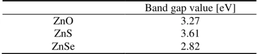
Perkin Elmer Lambda 25 UV-Vis Spectrometer between 300-1,100 nm wavelengths were used to carry out absorption studies to calculate the band gap of the semiconductor thin films. The band gap values of the produced semi-conductor thin films were calculated according to the Tauc Method [19]. (αhυ)2 vs. hυ plots are given in Figure 4.
The band gap values of the zinc-based thin films were determined from the point at which the linear part of the graph cuts the hυ axis. Table 1 showed that the band gap values of the zinc-based thin films.
Figure 4. The plots of (αhυ)2 vs. hυ of zinc-based thin films
(a)
(b)
(c)
(e)
(d)
(f)
15
15
15
15
15
15
1
1
1
1
1
1
Table 1. The band gap values of the zinc-based thin films
Band gap value [eV]
ZnO 3.27
ZnS 3.61
ZnSe 2.82
The calculated band gap values of the obtained thin films are close to the band gap of zinc-based semiconductors which are stated in the literature [20-22]. It has also been observed that the annealing process does not cause a change in the band gap values of zinc-based thin films.
CONCLUSION
The zinc-based semiconductor thin films have been deposited on glass substrates by CBD technique and annealed at 400 °C in air. The structural, morphological and optical properties of the obtained films have been specified. It has been seen that zinc-based thin films have polycrystalline nature and consist of nanoparticles. The band gap values of the produced thin films are close to the band gap of zinc-based semiconductors. It has also been observed that the annealing process does not cause any change in the structural, morphological and optical properties of zinc-based thin films. According to these results, zinc-based semiconductor thin films can be produced by CBD technique, which is a simple and economical technique. The most important point is that in this technique there is no need to anneal as in other thin film deposition techniques. This also provides energy savings.
ACKNOWLEDGMENT
Bilecik Seyh Edebali University Scientific Research Project Commission supported this work (project number is 2016-01.BŞEÜ.06-02).
NOMENCLATURE
Abbreviations
CBD Chemical Bath Deposition
FESEM Field Emission Scanning Electron Microscopy
FWHM Full Width at Half Maximum
ICDD The International Centre for Diffraction Data
RF Radio Frequency
XRD X-Ray Diffraction
UV-Vis Ultra Violet Visible
REFERENCES
1. Quoilin, S. and Orosz, M., Rural Electrification Through Decentralized Concentrating Solar Power: Technological and Socio-economic Aspects, J. Sustain.
Dev. Energy Water Environ. Syst., Vol. 1, No. 3, pp 199-212, 2013,
https://doi.org/10.13044/j.sdewes.2013.01.0015
2. Moser, M., Trieb, F. and Fichter, T., Potential of Concentrating Solar Power Plants for the Combined Production of Water and Electricity in MENA Countries,
J. Sustain. Dev. Energy Water Environ. Syst., Vol. 1, No. 2, pp 122-140, 2013,
https://doi.org/10.13044/j.sdewes.2013.01.0009
3. Sakata, I. and Sasaki, H., Bibliometric Analysis of International Collaboration in Wind and Solar Energy, J. Sustain. Dev. Energy Water Environ. Syst., Vol. 1, No. 3, pp 187-198, 2013, https://doi.org/10.13044/j.sdewes.2013.01.0014
4. Saib, S., Khan, M. A. and Bouarissa, N., Pressure-dependent Dynamical Properties of Zn-based II – VI Semiconductors, Phys. B: Condens. Matter., Vol. 407, No. 17, pp 3570-3574, 2012, https://doi.org/10.1016/j.physb.2012.05.027
5. Trivedi, S. B., Wang, C., Kutcher, S., Hommerich, U. and Palosz, W., Crystal Growth Technology of Binary and Ternary II – VI Semiconductors for Photonic Applications,
J. Crystal Growth, Vol. 310, No. 6, pp 1099-1106, 2008,
https://doi.org/10.1016/j.jcrysgro.2007.12.032
6. Khan, I., Ahmad, I., Aliabad, H. A. R. and Maqbool, M., DFT-mBJ Studies of the Band Structures of the II-VI Semiconductors, Materials Today: Proceedings, Vol. 2, No. 10, Part B, pp 5122-5127, 2015, https://doi.org/10.1016/j.matpr.2015.11.008 7. Goudarzi, A., Aval, G. M., Sahraei, R. and Ahmadpoor, H., Ammonia-free Chemical
Bath Deposition of Nanocrystalline ZnS Thin Film Buffer Layer for Solar Cells,
Thin Solid Films, Vol. 516, No. 15, pp 4953-4957, 2008,
https://doi.org/10.1016/j.tsf.2007.09.051
8. Caglar, M. and Yakuphanoglu, F., Structural and Optical Properties of Copper Doped ZnO Films Derived by Sol-Gel, Appl. Surf. Sci., Vol. 258, No. 7, pp 3039-3044, 2012, https://doi.org/10.1016/j.apsusc.2011.11.033
9. Firdaus, C. M., Shah Rizam, M. S. B., Rusop, M. and Rahmatul Hidayah, S., Characterization of ZnO and ZnO: TiO2 Thin Films Prepared by Sol-gel Spray-spin
Coating Technique, Procedia Eng., Vol. 41, pp 1367-1373, 2012, https://doi.org/10.1016/j.proeng.2012.07.323
10. O’Brien, S., Nolan, M. G., Çopuroglu, M., Hamilton, J. A., Povey, I., Pereira, L., Martins, R., Fortunato, E. and Pemble, M., Zinc Oxide Thin Films: Characterization and Potential Applications, Thin Solid Films, Vol. 518, No. 16, pp 4515-4519, 2010, https://doi.org/10.1016/j.tsf.2009.12.020
11. Lokhande, C. D., Pathan, H. M., Giersig, M. and Tributsch, H., Preparation of Znx(O,S)y Thin Films Using Modified Chemical Bath Deposition Method, Appl. Surf.
Sci., Vol. 187, No. 1-2, pp 101-107, 2002,
https://doi.org/10.1016/S0169-4332(01)00818-2
12. Pathak, T. K., Kumar, V., Purohit, L. P., Swart, H. C. and Kroon, R. E., Substrate Dependent Structural, Optical and Electrical Properties of ZnS Thin Films Grown by RF Sputtering, Phys. E: Low-Dimensional Syst. Nanostructures, Vol. 84, pp 530-536, 2016, https://doi.org/10.1016/j.physe.2016.06.020
13. Zedan, I. T., Azab, A. A. and El-menyawy, E. M., Structural, Morphological and Optical Properties of ZnSe Quantum Dot Thin Films, Spectrochimica Acta Part A:
Molecular and Biomolecular Spectroscopy, Vol. 154, pp 171-176, 2016,
https://doi.org/10.1016/j.saa.2015.10.016
14. Thirumavalavan, S., Mani, K. and Sagadevan, S., A Study of Structural, Morphological, Optical and Electrical Properties of Zinc Selenide (ZnSe) Thin Film,
Mater. Today: Proc., Vol. 3, No. 6, pp 2305-2314, 2016,
https://doi.org/10.1016/j.matpr.2016.04.141
15. Vyas, S., A Short Review on: Optimization Techniques of ZnO Based Thin Film Transistors, Chinese Journal of Physics, Vol. 56, No. 1, pp 117-124, 2018, https://doi.org/10.1016/j.cjph.2017.12.002
16. Temel, S., Influence of Deposition Temperature on Structural, Morphological and Optical Properties of ZnS Thin Films, Canadian Journal of Physics, Vol. 96, No. 7, pp 826-830, 2018, https://doi.org/10.1139/cjp-2017-0730
17. Acharyya, D. and Bhattacharyya, P., An Efficient BTX Sensor Based on ZnO Nanoflowers Grown by CBD Method, Solid-State Electronics, Vol. 106, pp 18-26, 2015, https://doi.org/10.1016/j.sse.2014.12.027
18. Temel, S., Gökmen, F. O., Yaman, E. and Nebi, M., Deposition and Characterization of ZnSe Nanocrystalline Thin Films, AIP Conference Proceedings, Vol. 1935, No. 1, pp 150002, 2018, https://doi.org/10.1063/1.5026008
20. Pati, S., Highly Textured ZnO Thin Films Grown Using Sol-gel Route for Gas Sensing Application, J. Alloys Compd., Vol. 695, pp 3552-3558, 2017, https://doi.org/10.1016/j.jallcom.2016.11.414
21. Qiu, K., Qiu, D., Cai, L., Li, S., Wu, W., Liang, Z. and Shen, H., Preparation of ZnS Thin Films and ZnS/p-Si Heterojunction Solar Cells, Mater. Latters, Vol. 198, pp 23-26, 2017, https://doi.org/10.1016/j.matlet.2017.03.171
22. Ashraf, M., Akhtar, S. M. J., Khan, A. F., Ali, Z. and Qayyum, A., Effect of Annealing on Structural and Optoelectronic Properties of Nanostructured ZnSe Thin Film, J. Alloys Compd., Vol. 509, No. 5, pp 2414-2419, 2011, https://doi.org/10.1016/j.jallcom.2010.11.032
Paper submitted: 09.03.2018 Paper revised: 31.07.2018 Paper accepted: 11.08.2018