Al
xGa
1−xN BASED SOLAR BLIND
SCHOTTKY PHOTODIODES
a thesis
submitted to the department of physics and the institute of engineering and science
of b˙Ilkent university
in partial fulfillment of the requirements for the degree of
master of science
By
Turgut Tut
January 2004
I certify that I have read this thesis and that in my opinion it is fully adequate, in scope and in quality, as a dissertation for the degree of Master of Science.
Prof. Ekmel ¨Ozbay (Supervisor) I certify that I have read this thesis and that in my opinion it is fully adequate, in scope and in quality, as a dissertation for the degree of Master of Science.
Assist. Prof. Ceyhun Bulutay I certify that I have read this thesis and that in my opinion it is fully adequate, in scope and in quality, as a dissertation for the degree of Master of Science.
Assist. Prof. ¨Ozg¨ur Akta¸s
Approved for the Institute of Engineering and Science:
Prof. Mehmet Baray,
Abstract
Al
xGa
1−xN BASED SOLAR BLIND SCHOTTKY
PHOTODIODES
Turgut Tut
M. S. in Physics
Supervisor: Prof. Ekmel ¨
Ozbay
January 2004
Photodetectors are essential components of optoelectronic integrated circuits and fiber optic communication systems. AlxGa1−xN is a promising material for optoelectronics and electronics. Applications include blue and green LEDs, blue laser diodes, high power-high frequency electronics, and UV photodetectors. Photodetectors that operate only in the λ < 280 nm spectrum are called solar-blind detectors due to their solar-blindness to solar radiation within the atmosphere. In this thesis, we present our efforts for the design, fabrication and characterization of Al0.38Ga62N/GaN based solar blind Schottky photodiodes. We obtained very low dark current, high quantum efficiency, high detectivity performance. Under 25 V reverse bias, we measured a maximum quantum efficiency of 71 percent at 254 nm and a maximum responsivity of 0.15 A/W at 253 nm for a 150 micron diameter device. To our knowledge, these are the best values reported in the literature. For a 30 micron device, 50 ps FWHM pulse response is observed. When the scope response is deconvoluted, a maximum 3-dB bandwidth of 4.0 GHz is obtained for 30 micron diameter Schottky photodiodes.
Keywords: Photodetector, Photodiode, Schottky Photodiode, Low Dark Current, Quantum Efficiency, High-Speed
¨
Ozet
Al
xGa
1−xN TABANLI G ¨
UNES
¸ K ¨
OR ¨
U SCHOTTKY
FOTOD˙IYOTLAR
Turgut Tut
Fizik Y¨uksek Lisans
Tez Y¨oneticisi: Prof. Ekmel ¨
Ozbay
Ocak 2004
Fotodetekt¨orler optoelectronik entegre devrelerin ve fiber optik haberle¸sme sistemlerinin ¨onemli elemanlarıdır. AlxGa1−xN optoelektronik ve elektronik uygulamalar i¸cin ¨onemli bir malzemedir. Mavi ve ye¸sil LED’ler, mavi lazer diyotlar, y¨uksek-g¨u¸c y¨uksek-frekans elektroniˇgi, ve UV fotodetekt¨orleri uygulama alanlarından sadece bir ka¸c tanesidir. Sadece 280 nm ve daha kısa dalga boylarındaki ı¸sıkla ¸calı¸san ve 280 nm’den daha uzun dalga boylarına kar¸sı duyarsız olan detekt¨orler g¨une¸s k¨or¨u fotodetekt¨orler olarak adlandırılırlar. Bu tezde
Al0.38Ga62N/GaN tabanlı gece k¨or¨u fotodetekt¨orlerin tasarım, fabrikasyon ve karakterizasyonuna ili¸skin yaptıˇgımız ¸calı¸smaları sunuyoruz. Yaptıˇgimız ¨ol¸cumlerde detekt¨orlerden ¸cok d¨u¸s¨uk karanlık akım, y¨uksek kuvantum verimi ve y¨uksek detektivite elde ettik. 150 mikron ¸caplı aygıtlardan 25 V ters voltajda ve 254 nm dalga boyunda y¨uzde 71 maximum quantum verimi ve 253 nm dalga boyunda maksimum 0.15 A/W responsivite elde ettik. Bildiˇgimiz kadarıyla bu deˇgerler bilimsel literat¨urde en iyi performans deˇgerlerine kar¸sılık gelmektedir. 30 mikron ¸caplı aygıtlarda 50 ps FWHM hız performansı g¨ozlenmi¸stir. Yine
aynı aygıt i¸cin osiloskopun ¨ol¸c¨um ¨uzerinde etkisi g¨oz¨on¨une alındıˇgında, maksi-mum 3-dB 4.0 GHz dalga geni¸sliˇgi elde edilmi¸stir.
Anahtar
s¨ozc¨ukler: Fotodetekt¨or, Fotodiyot, D¨u¸s¨uk Karanlık Akım, Kuvantum Verimi, Y¨uksek Hız.
Acknowledgement
I would like to express my deepest gratitude to Prof. Ekmel ¨Ozbay for his guidance, moral support, assistance, and patience during this research.
I would like to thank Necmi Bıyıklı as it was from him that I learned nearly everything concerning process and device characterization.
I would like to thank Bayram B¨ut¨un for his help in PECVD and Matlab programming.
I would like to address my special thanks to the past and present members of Advanced Research Laboratory, Physics Department and Electronics Department who helped to develop the experimental background of the process and device characterization facilities.
I would like to thank Feridun Ay for his help in writing in Latex.
A¸skın Kocaba¸s, Co¸skun Kocaba¸s, Ahmet Ender C¸ etiner, Sinem Binicioˇglu C¸ etiner, ˙Irfan Bulu, Deniz C¸ akır, Engin Durgun, Mustafa Karak¨ose, Cem Sevik, Yavuz ¨Ozt¨urk, Koray Aydın, Sefa Daˇg, Mehmet Bayındır, Ayhan Yurtsever, Sena S. Akarca Bıyıklı, H¨umeyra C¸ aˇglayan, Emre Ta¸sgın, and ˙Ibrahim Kimukin helped to keep my spirits high all the time which I appreciate very much.
I am indebted to my family for their continuous support and care.
Contents
Abstract i ¨ Ozet iii Acknowledgement v Contents viList of Figures viii
List of Tables x
1 Introduction 1
2 Theory of Photodiode Operation 4
2.1 Theoretical Background . . . 4 2.2 Photodiode Operation . . . 5 2.3 Schottky photodiodes . . . 5 2.4 P-I-N Photodiodes . . . 12 2.5 Diode Characteristics . . . 13 2.6 Current-Voltage Characteristics . . . 13 2.7 Quantum Efficiency . . . 13 2.8 Bandwidth . . . 14 2.9 Bandwidth-Efficiency Trade-off . . . 15 vi
3 Design 16 3.1 Optical Simulation . . . 16 3.2 Wafer Design . . . 22 4 Fabrication 26 4.1 Sample Preparation . . . 26 4.1.1 Normal Photolithography . . . 27
4.1.2 Image Reversal Photolithography . . . 27
4.1.3 Development . . . 28 4.2 Etching . . . 28 4.2.1 Wet Etching . . . 28 4.2.2 Dry Etching . . . 29 4.3 Metalization . . . 29 4.4 Annealing . . . 30
4.5 Plasma Enhanced Chemical Vapor Deposition (PECVD) . . . 32
4.6 Lift-off . . . 32
4.7 Photodiode Fabrication Process . . . 33
4.7.1 Ohmic Contact Formation . . . 34
4.7.2 Mesa Isolation . . . 35 4.7.3 Schottky Metalization . . . 36 4.7.4 Dielectric Deposition . . . 36 4.7.5 Interconnect Metalization . . . 37 5 Measurements 39 5.1 I-V Measurements . . . 39
5.2 Quantum Efficiency Measurements . . . 41
5.3 High Speed Measurements . . . 45
6 Achievements and Future Directions 48
List of Figures
2. 1 Energy band diagram of a Schottky contact . . . 6
2. 2 Photogenerated carriers drift to the Schottky and ohmic contacts under the electric field. . . 8
2. 3 The carriers generated at a depth W induces an output current during their transport across the depletion region. . . 9
2. 4 Time-dependence waveform of the induced current. . . 10
2. 5 Expected waveform of output current of a photodiode where hole drift velocity is smaller than electron drift velocity. . . 11
2. 6 p-i-n diode . . . 12
3. 1 Reflection and transmission of an electromagnetic wave incident on a dielectric film of thickness d2 . . . 17
3. 2 Reflectivity of 2 pairs of DBR on GaAs . . . 23
3. 3 Reflectivity of 2 pairs of DBR on GaAs . . . 23
3. 4 Reflectivity of 2 pairs of DBR on GaAs . . . 24
3. 5 Reflectivity of 8 pairs of DBR on GaAs . . . 24
4. 1 Wafer structure . . . 29
4. 2 Mesa profile of a 200 micron diameter device obtained by Dektak Profilometer . . . 30
4. 3 N+ and P+ ohmic contacts on a GaN based wafer sample fabricated via 3-step contact mask . . . 31
4. 4 Ohmic contacts after annealing . . . 32
4. 5 Cross section of the fabricated structure . . . 33
4. 6 Lift-off after Interconnect metalization . . . 34 viii
4. 7 N+ ohmic metalization in the highly doped GaN layer . . . 35
4. 8 N+ ohmic metalization after annealing . . . 35
4. 9 Mesa isolation after N+ ohmic contact formation . . . 36
4. 10Schottky metalization . . . 37
4. 11Silicon Nitride deposition . . . 37
4. 12A microphotograph of a complete device . . . 38
5. 1 I-V characteristics of a test pattern . . . 40
5. 2 I-V characteristics of a test pattern in semi-log scale . . . 41
5. 3 I-V characteristics of 30 micron diameter photodiode . . . 42
5. 4 Quantum Efficiency Setup . . . 44
5. 5 Quantum efficiency of a 150 micron diameter device under reverse bias . . . 44
5. 6 Responsivity of a 150 micron diameter device under 25 V reverse bias . . . 45
5. 7 Pulse response of a 30 micron diameter photodiode under 25 V reverse bias . . . 46
5. 8 Frequency response of a 30 micron diameter photodiode under 25 V reverse bias . . . 47
List of Tables
5.1 High speed measurement results for various Schottky photodiodes under 25 V reverse bias. . . 46
Chapter 1
Introduction
Photodetectors that operate only in the λ < 280 nm spectrum are called solar-blind detectors due to their blindness to solar radiation within the atmosphere [21].
The wide-bandgap semiconductor AlxGa1−xN has a direct bandgap between 3.4 eV to 6.2 eV, corresponding to ultraviolet (UV) absorption in the 365 nm to 200 nm range. Thus, AlxGa1−xN-based solid-state UV detectors can be tailored for UV detection for a variety of applications, including flame sensing for boilers and turbine engines (x=0-0.3) and solar-blind threat warning systems (x=0.4-0.5). The direct bandgap of AlxGa1−xN promises a sharp cut-off at the band-edge and high quantum efficiency, and the near lattice-match among AlxGa1−xN alloys offers the possibility of fabricating various heterostructures [2].
The advantage of UV flame sensing is based on the clear distinction in spectral characteristics between a flame and a hot refractory background. For wavelengths below 320 nm, UV emission from a gas flame is much more pronounced than a 1400 Co black body. Therefore, a UV sensitive photodetector can readily detect
the presence of flame against a bright, hot refractory. Traditionally, most flame-sensing devices are based on Gieger-Muller tubes that offer the advantages of high sensitivity and wide operating temperature range. However, they have drawbacks of being fragile, bulky, expensive, and high voltage users. Thus, an AlGaN -based solid-state UV detector is an attractive alternative to provide a low-cost,
CHAPTER 1. INTRODUCTION 2
low-voltage, and more reliable solution.
The solar-blind UV detection is attractive for missile threat warning applications. Due to the strong absorption of solar UV in the upper atmosphere (i.e., ozone absorption), detection in the 240 nm to 280 nm range is immune from solar interference. Traditionally, UV-sensitive photocathodes and electron multiplication stages are used to achieve the required sensitivity, but thus far no photocathodes have been found to have sufficient cut-off sharpness and long-wavelength suppression ratio. Therefore, expensive filters and optics must be employed. In addition, the low quantum efficiency of photocathodes and vacuum packaging make a solid-state solution desirable. The direct bandgap of
AlxGa1−xN promises a sharp long-wavelength cut-off at the band-edge, and a nearly unit-internal quantum efficiency (i.e., one electron-hole pair per photon). This compares well with a CsT e photocathode’s typical 0.1 to 0.3 quantum efficiency [1]. Due to its wide bandgap, intrinsic AlGaN has an extremely low thermal generation rate and virtually zero carrier concentration at room temperature (i.e., 10−23cm−3 for E
g=4eV). An extremely high dark impedance
and low noise can be obtained, even for uncooled devices.
For applications where photon counting capability is desired, current efforts in fabricating avalanche photodiodes (APD) are hampered, primarily by the high dislocation density in III-nitride materials and secondarily by the lack of good p-AlGaN and p-type ohmic contacts. Carrier trapping by point defects is also a significant problem. AlGaN photon counting devices based on the avalanche effect still face formidable challenges [2].
Several research groups have demonstrated a successful solar-blind operation with AlxGa1−xN photodetectors using photoconductive [3, 4], p-i-n [5, 15, 23], MSM [15, 16], and Schottky [17, 20, 21] detector structures. Cutoff wavelengths (λc) as short as ∼ 225 nm, an ultraviolet/visible rejection over 5 orders of
magnitude along with a responsivity of 0.12 A/W at 232 nm were reported by using Al0.7Ga0.3N p-i-n detector structures [6, 11]. Back illuminated p-i-n focal plane arrays have also been demonstrated [22]. Dark currents less than 2 pA at 30 V reverse bias and 3 dB bandwidth of 100 MHz were reported for an Al0.4Ga0.6N
CHAPTER 1. INTRODUCTION 3
MSM structure [16]. Al0.35Ga0.65N p-i-n photodiodes on SiC substrates with low leakage current were also successfully demonstrated [12].
We can fabricate Schottky photodiodes which do not require p-type doping. They are also easier to fabricate than p-i-n photodiodes. Besides the ease of fabrication, efficient collection of generated carriers within the junction, as well as high-frequency characteristics are the other advantages of AlGaN Schottky photodiodes. However, they have relatively low quantum efficiency mainly due to the optical absorption introduced by the thin Schottky metal, and exhibit high leakage currents and poor noise performance. The reported best detector performances obtained with solar-blind AlGaN Schottky photodiodes include a maximum responsivity of 0.07 A/W at 290 nm, a minimum λc of 278 nm and a
Chapter 2
Theory of Photodiode Operation
In this chapter, the theoretical backgrounds for p-n junctions, Schottky diode, and p-i-n diodes are given. Also the criteria for a good photodiode is discussed in terms of quantum efficiency and bandwidth.
2.1
Theoretical Background
Photodetectors can be separated into two classes : quantum detectors and thermal detectors. Thermal detectors respond to heating caused by the absorption of the incident radiation. The first requirement for thermal detectors is the heating effect which results in a temperature change. Also, this temperature change should yield a measurable change in a physical parameter such as resistance, capacitance etc. Thermopile, bolometer, pyroelectric, golay cell, and superconductor detectors are examples of thermal detectors. Thermal detectors can operate in a very broad spectral range. However, their bandwidth and sensitivity performances are relatively poor. The operation of quantum detectors is based on the photoeffect, in which the absorption of photons by some materials results in an electronic transition to a higher energy level and the generation of mobile charge carriers. Under the effect of an electric field, these carriers move and produce a measurable electric current. Photoemissive, photoconductive, and photovoltaic detectors are included in this category. Although quantum detectors
CHAPTER 2. THEORY OF PHOTODIODE OPERATION 5
have limited spectral response, they demonstrate high sensitivity and high speed which are very important for optical communication systems. In photoconductive detectors, when photons are absorbed by a semiconductor material, mobile charge carriers are generated (an electron-hole pair for every absorbed photon). The electrical conductivity of the material increases in proportion to the photon flux. An electric field applied to the material by an external voltage source causes the electrons and holes to be transported. This results in a measurable electric current in the circuit. As with photoconductive detectors, the photovoltaic detectors also known as photodiodes rely on photogenerated charge carriers for their operation. A photodiode is simply a p-n junction whose reverse current increases when it absorbs photons. p-n, p-i-n, Schottky photodiodes, and avalanche photodiodes (APD) are widely used photodetectors. When we apply a reverse bias high enough across a p-n junction, the high electric field in the depletion region (on the order of 106V /cm) can cause electrons to impact-ionize and this results in avalanche gain. Avalanche photodiodes can be used instead of photomultiplier tubes in photon counting applications. Operating principles of Schottky and p-i-n photodiodes are discussed in the following sections.
2.2
Photodiode Operation
When light is incident on a junction of a photodiode, photons having energy larger than or equal to the bandgap energy of the semiconductor are absorbed and excess electron-hole pairs are created and subsequently separated by the established electric field in the depletion region. Once the photodiode is connected through an external load in a circuit, a measurable current flows through the circuit which is proportional to the number of photons absorbed.
2.3
Schottky photodiodes
The theory of rectification in metal-semiconductor junction was developed in 1930 by W. Schottky who attributed rectification to a space-charge layer in the
CHAPTER 2. THEORY OF PHOTODIODE OPERATION 6
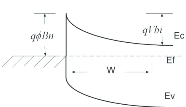
Figure 2. 1: Energy band diagram of a Schottky contact
semiconductor. A Schottky barrier is composed of metal and a semiconductor which are brought into intimate contact. When metal is deposited on a semiconductor in the thermal equilibrium, the Fermi levels of the two materials must be coincident.
The work function is the energy difference between the vacuum level and the Fermi level. This quantity is denoted by qφm for the metal and equal to
q(χ + V n) for the semiconductor. The potential difference between the metal
and the semiconductor work functions is called the contact potential. qφBn is called the barrier height and is equal to q(φm− χ). Under the abrupt junction
approximation that ρ ≈ qND for x < W ,
W =
s
2²
qND
(Vbi− V ) (2. 1)
Here ² is the dielectric constant of the semiconductor, ND is the ionized
donor atom density, Vbi is the built-in potential in the semiconductor, and V
is the applied potential to the junction. The current transport in the metal-semiconductor contacts is mainly due to majority carriers , in contrast to p-n junctions. There are mainly four different transport mechanisms : thermionic
CHAPTER 2. THEORY OF PHOTODIODE OPERATION 7
emission over the barrier, tunneling through the barrier, carrier recombination or generation in the depletion region, and carrier recombination in the neutral region of the semiconductor. Thermionic emission is the dominant transport mechanism, which gives rise to the ideal diode characteristics. Thermionic emission theory is derived by Bethe for high-mobility semiconductors, and diffusion theory is derived by Schottky for low-mobiliy semiconductors. Finally, a synthesis of the two approaches has been proposed by Crowell and Sze. The complete expression of the J-V characteristics is provided by the following equations.
J = Js(e qV kT − 1) (2. 2) Js = A∗∗T2exp(− qφBn kT ) (2. 3)
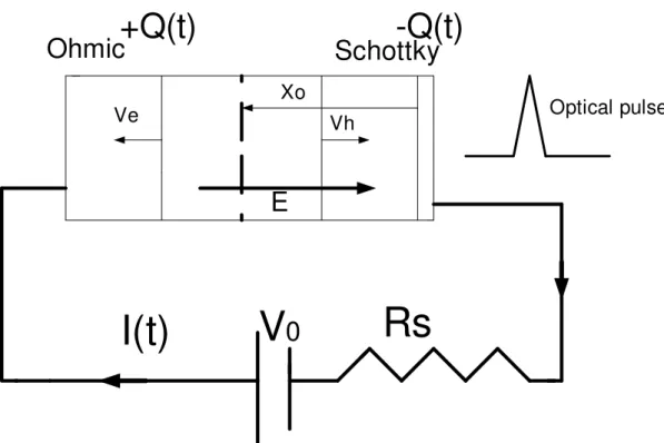
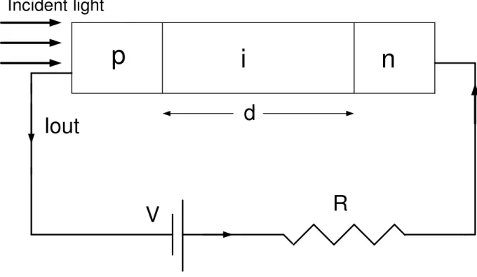
Schottky photodiodes can be used for the detection of UV and visible radiation and are the fastest of photodiodes available. However they have low quantum efficiency due to thin absorption regions and the highly absorbing Schottky metal. By applying sufficiently high reverse bias voltages, the entire N- region (active region) can be depleted, which results in a continuous electric field across the region. Photons with energies larger than the bandgap are absorbed in the depletion region and hole pairs are generated. The generated electron-hole pairs are swept away by the electric field. Electrons drift to the N+ doped semiconductor, holes drift to the Schottky metal and an output current is generated in the external circuit. The transport of carriers can be described using the diagram in Figure 2.3 [25, 31]. The depletion region can be considered as a parallel plate capacitor with a capacitance C = ²A
d where ² is the dielectric
constant, A is the diode area, and d is the depletion layer width. At the steady state, the voltage bias on the capacitor is V0, which results in a steady state total charge of Q0 across the capacitor, Q0 = CV0 . The electric field E varies with distance in the depletion region so we can express the applied bias voltage as,
V0 =
Z d
CHAPTER 2. THEORY OF PHOTODIODE OPERATION 8
N+
Ohmic
Schottky
E
hole electronIncident Light
R
V
Iout
Figure 2. 2: Photogenerated carriers drift to the Schottky and ohmic contacts under the electric field.
Here we assume that all the applied voltage appears across the depletion region. Let’s assume that, at t=0, a narrow optical pulse generates carriers with a total charge of q, at x0 from the Schottky contact as in Figure 2.3. Because of the established built-in electric field in the depletion region, electrons and holes drift in opposite directions in the form of charge sheets having surface charge density σ = Aq . The negatively charged sheet composed of electrons move away from the Schottky contact with drift velocity Ve, and a positively charged sheet
composed of holes moves towards the Schottky contact with drift velocity Vh.
Each sheet contributes to the electric field formed between the sheets equally as,
Eσ =
σ
² (2. 5)
And this electric field is opposite to the depletion layer electric field, which results in a voltage drop across the depletion region as the charged sheets move
CHAPTER 2. THEORY OF PHOTODIODE OPERATION 9
Ohmic
Schottky
E
Rs
V
0
I(t)
-Q(t)
+Q(t)
Optical pulse Vh Ve XoFigure 2. 3: The carriers generated at a depth W induces an output current during their transport across the depletion region.
away from each other. This time dependent voltage can be expressed as:
Vσ =
Z xe(t)
xh(t) Eσdx = Eσ[xe(t) − xh(t)] (2. 6)
where these time dependent coordinates can be expressed as:
Xe(t) = X0+ ve(t), 0 < t < te (2. 7)
Xh(t) = X0− vh(t), 0 < t < th (2. 8)
where te = d−xve0 and th = xvh0 are electron and hole transit time, defined as the
time required for the carriers to complete their transport. Assuming te> th , we
CHAPTER 2. THEORY OF PHOTODIODE OPERATION 10
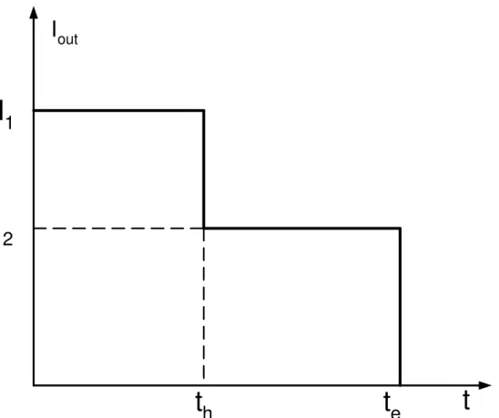
I
outt
t
h
t
e
I
1
I
2
Figure 2. 4: Time-dependence waveform of the induced current.
Vσ(t) = σ ²(ve+ vh)t 0 < t < th σ ²vet th < t < te (2. 9)
Iout(t) can be expressed as,
Iout(t) = dQ(t) dt = d dt[CV (t)] (2. 10) where V (t) = V0− Vσ, so Iout(t) is : Iout(t) = I1 = qd(ve+ vh) 0 < t < th I2 = qdve th < t < te (2. 11) Using this result we can obtain the output current for different absorption situations. We can assume that the absorption over the depletion layer is
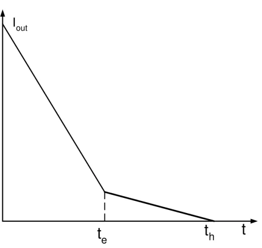
CHAPTER 2. THEORY OF PHOTODIODE OPERATION 11
I
outt
t
h
t
e
Figure 2. 5: Expected waveform of output current of a photodiode where hole drift velocity is smaller than electron drift velocity.
constant, and the hole drift velocity is smaller than electron drift velocity. Under this assumption, when all electrons reach the end of the depletion layer, there exist some holes that contribute to the total current. Therefore, the current flows until all the holes leave the depletion layer. Current output of such a device can be seen in Figure 2.5. We can also assume that the absorption constant is so high that all the incident light is absorbed near the Schottky contact. In this case the current output is a square that continues until te .
CHAPTER 2. THEORY OF PHOTODIODE OPERATION 12
i
p
n
d
Iout
R
V
Incident light
Figure 2. 6: p-i-n diode
2.4
P-I-N Photodiodes
A p-i-n photodiode is simply a p-n junction with an intrinsic layer sandwiched between p and n type doped layers. It operates in reverse bias mode and it is suitable for high quantum efficiency operation due to its intrinsic layer. However, generally homojunction p-i-n photodiodes lack in high-speed operation because there is a diffusion component in the output current. The photogenerated carriers outside the depletion region diffuse to the intrinsic i region and in the depletion region they are swept away by the electric field. Since diffusing is slower than drifting in high electric field, p-i-n photodiodes are much slower than Schottky photodiodes. This problem can be solved by using p and n layers which have higher band gaps than intrinsic layers, so that photogeneration occurs only in the intrinsic region. In this way, high efficiency and high speed p-i-n photodiodes can be designed.
CHAPTER 2. THEORY OF PHOTODIODE OPERATION 13
2.5
Diode Characteristics
Photodiode characterization is composed of I-V (current-voltage) measurement, quantum efficiency, and high speed (bandwidth) measurements. Performance of a photodiode is tested via these characterizations.
2.6
Current-Voltage Characteristics
As an electronic device, the photodiode has an I-V relation given by
I = Is[exp(
eV nkBT
) − 1] − Ip (2. 12)
where n is the ideality factor, Ip is the photocurrent proportional to the photon
flux [31].
Low dark current and high breakdown voltage are two parameters that determine the photodiode quality. Dark current is the current flowing in the reverse bias with no light illumination. A device with lower dark current is likely to be more sensitive. We can not apply a reverse bias voltage (as high as we would like) across a photodetector, because after a certain voltage photodiode enters into breakdown. This limits the reverse bias voltage that can be applied for photodiode operation.
2.7
Quantum Efficiency
The quantum efficiency η (0 ≤ η ≤ 1) of a photodetector is defined as the probability that a single photon incident on the device generates a photocarrier pair that contributes to the detector current. When many photons are incident, as is almost always the case, η is the ratio of the flux of generated electron-hole pairs that contribute to the detector current to the flux of incident photons. Incident photons do not produce electron-hole pairs, because some of the incident photons are not absorbed. These photons may be reflected from the surface of the photodetector. Photogenerated pairs near the surface may recombine due
CHAPTER 2. THEORY OF PHOTODIODE OPERATION 14
to the abundant recombination centers and they will fail to contribute to the photocurrent [31].
The quantum efficiency can therefore be expressed as:
η = (1 − R)ζ[1 − exp(−αd)] (2. 13)
where R is the front surface reflectivity, α is the power absorption coefficient, d is the thickness of the absorbing semiconductor layer, and ζ is the fraction of electron-hole pairs that contribute to the detector current [31].
2.8
Bandwidth
As mentioned previously, the response time of a photodetector is mainly limited by the transit times of the photogenerated carriers. RC time constant of the photodiode circuit and diffusion of carriers in the undepleted regions also impose limitations on the response time of a photodetector.
Schottky and heterojunction photodetector designs can be used to resolve the carrier diffusion problem either by decreasing the undepleted regions as in Schottky diodes or using different band gap materials as in heterojunction photodiodes.
When we decrease d (depletion width), the capacitance of the junction increases. This in turn increases the transit time. The transit time and capacitance limited 3 dB bandwidths can be expressed as:
ftr = 0.45 v d (2. 14) fRC = d 2πR²A (2. 15)
By decreasing d we can increase the bandwidth as long as we use small devices so that the capacitance of the devices decreases accordingly. So if we consider only the transit time limitation, the bandwidth of the photodetector is inversely proportional to d [29].
CHAPTER 2. THEORY OF PHOTODIODE OPERATION 15
2.9
Bandwidth-Efficiency Trade-off
The bandwidth-efficiency product determines the overall performance of a photodiode. Bandwidth and efficiency have inverse dependencies on active layer thickness, d. High quantum efficiencies near unity and bandwidth can be achieved with very thick and very thin active layers respectively but their product for a given d is almost constant [29]. The bandwidth-efficiency product can be increased by using resonant cavity enhancement effect (RCE) [32].
Chapter 3
Design
In this chapter, we will demonstrate how we optimized the performance of our Schottky diodes by using optical simulation. This will be followed by a discussion of the wafer structure.
3.1
Optical Simulation
In this chapter we will study the reflection and refraction of electromagnetic waves from an interface separating two media and from a stack of films. Such studies are very important in understanding many practical optical devices such as Fabry-Perot etalons, special optical coatings, double brag mirror (DBR) etc.
Assuming the incident light is in the form of polarized plane waves and it is vertical to the plane of interface between the two media, we can write the electric field vector as,
~
E = ~E0e(ωt−i~k·~r). (3. 1)
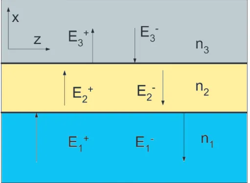
Therefore, for Fig.3.1 we can write the electric fields in the three regions as the following,
CHAPTER 3. DESIGN 17
Figure 3. 1: Reflection and transmission of an electromagnetic wave incident on a dielectric film of thickness d2
E = ˆ yE1+e−ik1x+ ˆyE1−eik1x; x < 0 ˆ yE2+e−ik2x+ ˆyE2−eik2x; 0 < x < d2 ˆ yE3+eik3d2e−ik3x+ ˆyE3−e−ik3d2eik3x; x > d2 (3. 2) where ki = ( ω c)ni = k0ni; i = 1, 2, 3 (3. 3) n1, n2, and n3 being the refractive indices and
k0 = ω c = 2π λ0 (3. 4) denotes the free space wave number. The implicit eiωt time dependence has
been suppressed and therefore the superscripts + and - correspond to waves propagating in the +x and -x directions respectively.
The corresponding magnetic fields can be calculated by using the formula H = k × E
CHAPTER 3. DESIGN 18
and are given by
H = ˆ zn1 cµ0E1 +e−ik1x− ˆz n1 cµ0E1 −eik1x; x < 0 ˆ zn2 cµ0E2 +e−ik2x− ˆz n2 cµ0E2 −eik2x; 0 < x < d 2 ˆ zn3 cµ0E3 +eik3d2e−ik3x− ˆz n3 cµ0E3 −e−ik3d2eik3x; x > d 2 (3. 6)
where the media are assumed to be nonmagnetic with µ = µ0. Since both E and H represent tangential components, they must be continuous at x = 0 and at
x = d2 . Continuity at x=0 gives us E1++ E1− = E2++ E2− (3. 7) n1(E1+− E1−) = n2(E2+− E2−) (3. 8) E1+ E− 1 = S1 E2+ E− 2 = 1 t1 1 r1 r1 1 E2+ E− 2 (3. 9)
where r1 and t1 are the amplitude reflection and transmission coefficients at the first interface and given by
r1 = n1− n2 n1+ n2 (3. 10) t1 = 2n1 n1+ n2 (3. 11) Continuity of the fields at x = d2 readily gives us
E + 2 E− 2 = S2 E + 3 E− 3 = 1 t2 eiδ2 r2eiδ2 r2e−iδ2 e−iδ2 E + 3 E− 3 (3. 12)
where r2 and t2 are once again the amplitude reflection and transmission coefficients at the second interface
CHAPTER 3. DESIGN 19 E + 1 E− 1 = S E + 3 E− 3 = a b c d E + 3 E− 3 (3. 13)
Now in the third medium there will not be any reflected wave and as such
E−
3 = 0. This immediately gives us
E+
1 = aE3+ (3. 14)
E1− = cE3+ (3. 15)
and therefore the amplitude reflection and transmission coefficients of the film are given by r = E − 1 E+ 1 = c a (3. 16) t = E + 3 E1+ = 1 a (3. 17) R = |r|2 = r21+ r22+ 2r1r2cos 2δ2 1 + r2 1r22+ 2r1r2cos 2δ2 (3. 18) T = |t|2n3 n1 = n3 n1 t2 1t22 1 + r2 1r22+ 2r1r2cos 2δ2 (3. 19) upon substituting the related values for r and t , we obtain
R + T = 1 (3. 20)
Furthermore when cos 2δ2 = −1, i.e., when δ2 = (m + 12)π; m = 0, 1, 2, .... or d2 = 4nλ02,3λ4n02,5λ4n02, .... minimum reflectivity is achieved (for r1r2 > 0) and it is given by R = µ r 1− r2 1 − r1r2 ¶2 = Ã n1n3− n22 n1n3+ n22 !2 (3. 21) Thus the reflectivity will be zero when n2 = (n1n3)
1
2. The reflectivity of the surface can be made zero at any chosen wavelength λc by choosing the film
CHAPTER 3. DESIGN 20
thickness to be λc
4n2. This technique of reducing the reflectivity of a surface is known as blooming and the surface is said to be antireflected coated.
When cos 2δ2 = 1 i.e., when d2 = 2nλ02,2n2λ02,3λ2n02.... the reflectivity is given by
R = µn 3− n1 n3+ n1 ¶2 (3. 22) which is independent of the refractive index of the intermediate film.
For the case of two films, the expression for the fields in the first three regions are given by Eqn.3.1 and 3.5; in region 4 the fields are given by
E = ˆyE4+eik4(d2+d3)e−ik4x+ ˆyE− 4 e−ik4(d2+d3)eik4x (3. 23) H = ˆz n4 cµ0 E+ 4 eik4(d2+d3)e−ik4x− ˆz n4 cµ0 E− 4e−ik4(d2+d3)eik4x (3. 24) Continuity of the fields at x = d2+ d3 gives us
E + 3 E− 3 = S3 E + 4 E− 4 = 1 t3 eiδ3 r3eiδ3 r3e−iδ3 e−iδ3 E + 4 E− 4 (3. 25)
where r3 and t3 are the amplitudes of reflection and transmission coefficients between media 3 and 4 and
δ3 = k3d3 = ( 2π λ0 )n3d3 (3. 26) thus E + 1 E− 1 = S E + 4 E− 4 (3. 27) where S = S1S2S3 (3. 28)
Similarly one can readily obtain expressions for reflectivity and transmittivity. Generalizing the above analysis for N films and for oblique incidence, we may write
CHAPTER 3. DESIGN 21 E + 1 E− 1 = S E + N +2 E− N +2 (3. 29) where S = S1S2...SN +1 (3. 30) and Sj = 1 tj eiδj rjeiδj rje−iδj e−iδj (3. 31) δ1 = 0 δj = kjdjcos θj = ( 2π λ0 )njdjcos θj; j = 2, 3, ..., (N + 1) (3. 32)
and rj and tj are the amplitude reflection and transmission coefficients between
media with refractive indices nj and nj+1.
Using Snell’s law δj can also be expressed as,
δj = ( 2π λ0 )dj(n2j − n21sin2θ1) 1 2. (3. 33)
By using the angle of incidence at the first interface namely θ1, δj can readily
be calculated [33]. This method can be used to calculate the transmission and reflection or absorption at any layer and is called the transfer matrix method (TMM).
Although metals are good reflectors, their reflectivities (R ≤ %96 for thick layers) are not high enough , and vary with spectrum [30]. The main drawback of metal mirrors is that they absorb at the optical wavelengths, therefore very thin layers must be used.
Distributed Bragg Mirrors (DBR’s) are widely used in optoelectronic applications such as detectors and semiconductor lasers. A DBR is a stack consisting of periodically alternating quarter-wave thick material layer pairs whose refractive indices are different at the wavelength region of interest. Each pair consists of two layers having thicknesses of λc/4n1 and λc/4n2 respectively
CHAPTER 3. DESIGN 22
and λc is the central wavelength of the mirror where reflectivity is maximum.All
the light reflected from different interfaces of the DBR has the same phase resulting in constructive interference therefore we have very high reflectivity. Using the TMM method for a DBR consisting of N pairs, the reflectivity at the center wavelength can be expressed as,
Rmax = Ã n2N 1 − n2N2 n2N 1 + n2N2 !2 (3. 34) This formula is valid when the stack is in the air, but for the first and the last layers which are different from air, we have to modify the formula as,
Rmax = n0 ns( nL nH) 2N − 1 n0 ns( nL nH) 2N + 1 2 (3. 35) where n0 and ns are refractive indices of air and substrate medium [34]. We
assume that the thickness of the substrate layer is infinite, since it is significantly thicker than the other layers in the wafer structure. We can illustrate this situation by growing DBR pairs consisting of SiO2 and Si3N4 since at 350 nm
Si3N4 is grown on SiO2 to have an enhancement in reflectivity. If we reverse the order, reflectivity decreases at the center wavelength. The appropriate thickness for DBR layers can be calculated using the formula λc
4n, where n is the layer’s refractive index at λc . For λc=350 nm, this results in thicknesses of 49.7 nm
and 59.5 nm for Si3N4 and SiO2 respectively. By increasing the number of DBR pairs we can obtain reflectivities that are very close to unity.
3.2
Wafer Design
The epitaxial structure of the front-illuminated Schottky detector wafer was designed to achieve true solar-blindness, low leakage , and high solar rejection. In order to meet these requirements, Al0.38Ga0.62N absorption layer was used to achieve λc < 280 nm. The AlxGa1−xN/GaN epitaxial layers of our heterojunction Schottky photodiode wafer were grown on a 2-inch single-side polished (0001) sapphire substrate using metalorganic chemical vapor deposition
CHAPTER 3. DESIGN 23
Figure 3. 2: Reflectivity of 2 pairs of DBR on GaAs
Figure 3. 3: Reflectivity of 2 pairs of DBR on GaAs
(MOCVD). Since AlGaN based structures do not have their own substrate, we have to lattice match the structure by growing very thin materials whose lattice parameters are very close to the surrounding layer materials. Therefore, a thin AlN nucleation layer was first grown followed by a 0.5 µm thick
CHAPTER 3. DESIGN 24
Figure 3. 4: Reflectivity of 2 pairs of DBR on GaAs
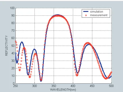
Figure 3. 5: Reflectivity of 8 pairs of DBR on GaAs
unintentionally doped GaN mesa isolation layer. Afterwards, a highly doped (n+ = 2x1018cm−3) ohmic contact layer composed of 0.6 µm thick GaN and 0.2
µm thick Al0.38Ga0.62N were grown, respectively. The growth of the Schottky heterostructure was completed with the deposition of a 0.8 µm thick undoped
CHAPTER 3. DESIGN 25
Al0.38Ga0.62N active layer. The highly doped GaN layer was used for ohmic contact region due to the difficulty of obtaining high-quality ohmic contacts with
AlxGa1−xN/GaN layers. The n-type doped 0.2 µm thick Al0.38Ga0.62N layer was used as a diffusion barrier for the photocarriers generated in the GaN ohmic contact layer. Such a diffusion barrier is expected to increase the solar-blind/near-UV rejection ratio of the detector [21].
Chapter 4
Fabrication
Our fabrication processes are carried out in a class 100 clean-room at the Advanced Research Laboratory of the Physics Department, which has a dust count of 100 particles per cubic foot volume. This corresponds to 3500 particles (with particles diameters of 0.5 µ or larger) per cubic meter [35].
4.1
Sample Preparation
First, we cleave the wafer to obtain a sample large enough to handle but not too large since the epitaxial wafers are very expensive. The mask size is 7x7 mm2. The cleanness of the sample, the chemicals used, and the environment are very important for successful fabrication. To cleave the wafer, we use a diamond tipped scriber-pen. After defining the line of the cut on the back surface of the wafer which is not polished, we press the scriber’s tip at the edge of the wafer. Unfortunately it is not easy to obtain GaN , or AlxGa1−xN wafers in the desired size or shape. When the scriber’s tip is pressed on the wafer, it may crack into various miniscule pieces. Therefore the samples are difficult to handle and process.
At the beginning of every step we have to do a three-solvent-cleaning (TCS) process. Trichloroethane dissolves oil, acetone dissolves photoresist, organic molecules and trichloroethane, and isopropanol dissolves acetone, and water
CHAPTER 4. FABRICATION 27
dissolves the acetone. Samples are placed into a teflon basket and immersed into boiling trichloroethane for 2 minutes, then into acetone at room temperature for 5 minutes, then into boiling isopropanol for 2 minutes. Samples are exposed to the deionized water(DI) flow and then dried with a nitrogen gun.
Samples are baked on a hot plate at 120 oC for 2 minutes which is called
dehydration bake. Finally the samples’ surfaces are examined under an optical microscope.
4.1.1
Normal Photolithography
AZ 5214E type photoresist has an absorption peak at around 360 nm and we perform the UV exposure with an Hg lamp which has a line at 365 nm. Mask alignment is done with a Karl-Suss MJB3 mask aligner. Mask alignment is accomplished by means of alignment marks. After pre-bake, the sample is aligned with the mask. Then the sample is exposed to UV radiation for 20 seconds with an optical power of 8 mW/cm2 for a total dose of 160 mJ/cm2.
4.1.2
Image Reversal Photolithography
In this technique the transparent parts of the mask will be transferred onto the resist, so that the mask is different from the mask used in normal lithography. The resist covered sample is aligned with the image-reversed mask and exposed with an optical power of 8 mW/cm2 for 8 seconds. Then the sample is baked for 2 minutes at 110 oC on a hot plate. The sample is exposed for 18 seconds
without mask which is called flood exposure. These two additional processes change the photoresist, so that the first exposed regions behave as non-exposed regions and vice versa. Therefore the additional bake is very critical in image reversal lithography. The optimization is done by changing the image reversal bake time and the bake temperature. Image reversal photolithography makes the liftoff of thick metallization easy. Normally, the exposure is larger near the top of any resist, which results in a more rapid development near the surface and leads to a resist profile with a positive slope for positive resists. However, after image
CHAPTER 4. FABRICATION 28
reversal this profile is also reversed, resulting in an undercut profile.
4.1.3
Development
AZ 400K developer is used with a 1:4 ratio of developer to DI water for the development of the exposed samples. In the normal photolithography the exposed regions of resist are etched while in the image reversal photolithography the non-exposed regions are etched. The development time is determined by using a dummy GaAs sample since we cannot observe the color change on a GaN or
AlxGa1−xN sample since it is transparent. In development we use a white basket to observe the color change easily. When the color change has stopped, the samples are rinsed under DI water flow. By this method, we find the development time to be ∼ 43 − 47 seconds with a thickness of ∼ 1.4 µ. Then the sample is dried with a nitrogen gun. The samples are placed under an optical microscope, the resolution patterns should be sharp and 1 µ resolution should be observed for a good photolithography. Mask alignment is observed via the alignment marks.
4.2
Etching
In processing the wafer, we have to etch through the wafer surface. For example, we have to make contacts to an epitaxial layer buried under the surface of the wafer, second we must isolate devices by making mesas, third to make contacts to metalizations beneath the silicon nitride. Etching can be divided into wet (aqueous solution) etching and dry etching (Reactive Ion Etching).
4.2.1
Wet Etching
Chemical solvents are used to wet etch semiconductor and dielectric materials.
GaAs etchant is first to oxidize the surface with an oxidizing agent and second
to remove the oxidized layer with acid or base. In our processes we use
H2O2/NH3/H2O (2.4:8:300) as an etchant with an etch rate of 50 Ao/sec. at room temperature. Dielectric materials SiO2, Si3N4 can be etched with HF .
CHAPTER 4. FABRICATION 29
0.8 micron Al0.38Ga 0.62N N- ~1016cm-3
0.2 micron Al0.38Ga0.62N N+ ~2x1018cm-3
0.6 micron GaN N+ ~2x1018cm-3
0.5 micron GaN undoped sapphire undoped
Figure 4. 1: Wafer structure
IT O can also be etched via HF . HF in its aqueous form is very dangerous and
it should be handled very carefully. We use a diluted HF / DI water (1:30) in silicon nitride etching at a rate of 400 Ao/sec..
4.2.2
Dry Etching
We use an ultra high vacuum RIE machine for dry etching. Photoresist and dielectric materials are etched with plasma ions hitting the sample surface. Using various gases in the plasma we can etch different materials. O2 is used to etch photoresist film. CCl2F2 etches SiO2, Si3N4, and IT O. Si3N4 can also be etched with CHF3. In our fabrication GaN and AlxGa1−xN are etched with CCl2F2.
4.3
Metalization
In our processes we use the lift-off metallization technique to make ohmic and Schottky contacts, and the interconnects between them. Once the required metallization layout is defined by photolithography, the samples are coated with the desired metals. Since the photoresist film has a finite thickness, the coated material (if it is thin enough) is discontinuous at the pattern edges of the resist. Therefore, in acetone the photoresist dissolves lifting off the material that is on it. The metals are deposited onto the samples via UHV LE590 box coater. Metals in powder or solid form are placed in tungsten boats. UHV causes the metal to
CHAPTER 4. FABRICATION 30
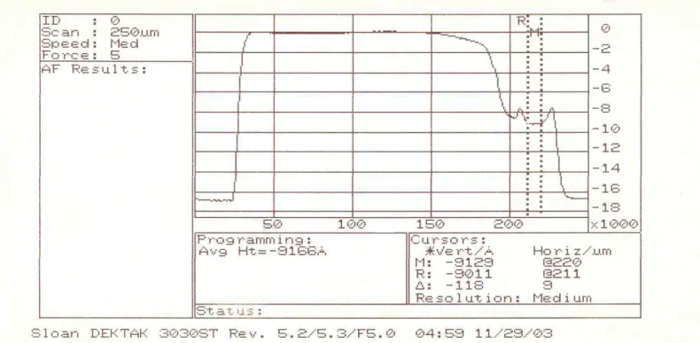
Figure 4. 2: Mesa profile of a 200 micron diameter device obtained by Dektak Profilometer
evaporate in lower temperatures. From Fig.4.3 one can see the ohmic contacts on a GaN based wafer sample. This sample is fabricated by using a three-step contact mask. We make the metalic contacts to the sample and try to find the optimum temperature and RTP time for good ohmic contacts.
Samples are placed over the boats. Short holder is used to decrease the usage of metals but we have to be careful watching the sensors display since the holder is half of the long holder and the actual deposition rate is four times the displayed value. When the desired pressure is reached, current is passed through the tungsten boats and metal deposition takes place.
4.4
Annealing
To make metal semiconductor contacts ohmic we use rapid thermal process (RTP) in which samples are heated to very high temperatures in a very short
CHAPTER 4. FABRICATION 31
Figure 4. 3: N+ and P+ ohmic contacts on a GaN based wafer sample fabricated via 3-step contact mask
time. Within 30 − 60 seconds, the metal contact melts and diffuses into the semiconductor and the barrier that electrons encounter becomes very low and as a result the contact resistance becomes ohmic. Flash lamps are used as the heating source. From Fig.4.4, one can notice the cheese like structure on the ohmic contact which is an indicator of a good ohmic contact.
CHAPTER 4. FABRICATION 32
Figure 4. 4: Ohmic contacts after annealing
4.5
Plasma Enhanced Chemical Vapor
Deposi-tion (PECVD)
Dielectric films are used mainly to protect the devices on the wafer. Silicon nitride films can be used for passivating devices, because they serve as barriers to the diffusion of water and sodium. Silicon nitride oxidizes very slowly and prevents the underlying layers from oxidation. In our processes, PECVD is used to deposit silicon nitride and silicon oxide at relatively low temperatures with respect to other methods. Otherwise, high temperatures can affect the ohmic contacts. Dielectric coatings can also be used as anti-reflection or reflection coatings. To deposit Si3N4, we used silane (2%SiH4+ 98%N2) and ammonia ( NH3) gases at 250oC at a deposition rate ∼ 140Ao/min.
4.6
Lift-off
After metalization, the sample is left in acetone. Acetone dissolves the photoresist and the metal deposited on the photoresist lifts off. However, the metal on the
CHAPTER 4. FABRICATION 33 0.8µm Al0.38Ga0.62N N - ~1016cm-3 0.2 µm Al0.38Ga0.62N N+ ~2x1018cm-3 0.6 µm GaN N+ ~2x1018cm-3 0.5 µm Undoped GaN
Sapphire Substrate
10nm Ti/0.7 µm Au Interconnect 10nmTi/100nmAl ~400 AoSi 3N4 100 AoAu SchottkyFigure 4. 5: Cross section of the fabricated structure
open area of the resist will remain on the sample surface. In order to obtain a good lift-off we should wait a few hours and if the lift- off is not complete we should spray the sample with acetone. In the case of thick metallization ( > 1 µ) we may need ultrasound application. However this is a bit as risky it may remove the metal which should stay on the sample surface. Therefore ultrasound must only be applied for a short duration, e.g. a few seconds.From Fig.4.6, one can see the interconnect pads after a good lift-off.
4.7
Photodiode Fabrication Process
Schottky diode fabrication is a five-step process which is described below. The device structure can be seen in Fig.4.5.
CHAPTER 4. FABRICATION 34
Figure 4. 6: Lift-off after Interconnect metalization
4.7.1
Ohmic Contact Formation
After a normal photolithography, we have to reach the N+ ohmic layer. This task is done via reactive ion etching (RIE) under CCl2F2 plasma, 20 sccm gas flow rate, 8x10⁻³ mBar pressure, and 100W RF power. The etch rates for GaN
and Al0.38Ga0.62N layers are determined as 300 and 140 Ao/min., respectively. After an ohmic etch of ∼ 1.3 µm, T i/Al (100 Ao /1000 Ao) contacts are deposited
via thermal evaporation and left in an acetone solution for lift-off process. To make sure that we reach the N+ ohmic layer, we use DekTak stylus profilometer. We anneal the contacts at 700 oC for 30 seconds in a rapid thermal annealing
(RTP) system. We optimize the temperature for ohmic contact by varying the temperature on another sample with ohmic contact mask which is a three-step process. In Figure 4.7, one can notice the long crack line in the ohmic contact metalization surface before annealing. As shown in Figure 4.8, a white cheese like pattern is formed on the ohmic contact surface.
CHAPTER 4. FABRICATION 35
Figure 4. 7: N+ ohmic metalization in the highly doped GaN layer
Figure 4. 8: N+ ohmic metalization after annealing
4.7.2
Mesa Isolation
After a normal PL, we etch all sample surfaces except for the diode active regions called mesas. In order to isolate these active regions we have to reach the undoped layer under the N+ ohmic layer. Mesa structures of the devices are formed via the same RIE process, by etching all the layers (∼1.6 µm) down to the undoped
GaN mesa isolation layer. The etch depth is monitored using a DekTak stylus
profilometer. As can be seen from Figure 4.2 after ohmic contacts are deposited and mesa etch is completed the etch depths are at the desired level. From Fig.4.9, one can notice the height difference between the mesa of the device and the sample
CHAPTER 4. FABRICATION 36
Figure 4. 9: Mesa isolation after N+ ohmic contact formation lower level which is undoped GaN.
4.7.3
Schottky Metalization
After normal PL with a Schottky mask, a ∼ 100 Ao thick Au film is deposited
to form the Au/AlGaN Schottky contacts. The Schottky contact can be seen in Fig.4.10.
4.7.4
Dielectric Deposition
We deposited λ
4n thick Si3N4 thin film over the entire sample surface. After a normal PL and wet etching ( HF :H2O = 1:30) for ∼ 3 seconds, nitride film is removed from the resist openings for the ends of interconnect pads. The etched areas are checked under an optical microscope. Thin nitride film acts as anti-reflection coating and protects the Schottky metal from the atmosphere and scratching. Figure 4.11 shows the color change over the entire surface of the device.
CHAPTER 4. FABRICATION 37
Figure 4. 10: Schottky metalization
Figure 4. 11: Silicon Nitride deposition
4.7.5
Interconnect Metalization
Finally, a ∼ 0.7 µm thick T i/Au interconnect metal is deposited and lifted off to connect the Schottky layers and N+ ohmic contacts to coplanar waveguide transmission line pads. In Figure 4.12, one can see the interconnect pads touching
CHAPTER 4. FABRICATION 38
Figure 4. 12: A microphotograph of a complete device
the ohmic and Schottky contacts. We apply bias through these interconnect pads.
Chapter 5
Measurements
In this chapter, we present measurements performed on the fabricated pho-todiodes. Except high speed measurements, all measurements are conducted at the Bilkent Advanced Research Laboratory. High speed measurements are performed at the Electrical and Electronics Engineering Department. Although its presentation may seem short, characterization takes more time than the fabrication of the devices. For example we have to optimize the setup, find the best parameters such as delay time for low level dark current measurement, we have to find the optimum angle for the fiber to focus the light onto the thin Schottky metal surface, and we have to check nearly 100 devices on the sample surface.
5.1
I-V Measurements
After the devices are fabracated, we make the characterization of our photodiodes. The first check of the process is the I-V test of the finished photodiodes. A good Schottky photodiode should have high reverse breakdown voltage , low dark current, and low turn-on voltage.
We used an HP 4142B Modulator DC Source/Monitor analyzer in our I-V measurements. We find out that it does not have enough resolution to measure the dark current of our devices. So we measure the dark current of the devices
CHAPTER 5. MEASUREMENTS 40
-70 -60 -50 -40 -30 -20 -10 0
10 20 30
-150
-100
-50
0
50
100
150
200
D
a
rk
C
u
rr
e
n
t
(p
A
)
Applied Voltage(V)
Figure 5. 1: I-V characteristics of a test pattern
with Keithley 6517A electrometer, which can measure currents on the order of femto-amperes. In all I-V measurements, we use the probe station. From Fig. 5.2, one can notice that for a test pattern having 100x100 micron square area device, we measured 33 fA dark current for 25 V reverse bias. At 70 V reverse bias, we measured ∼ 200 pA dark current for the same device. For 30 micron diameter device, we measured ∼ 10 pico-amperes for ∼ 20 V reverse bias. This can be seen from Fig.5.3.
From our measurements, we also find that as the area of the Schottky diodes increases, the dark current increases. That is an expected result because, as the device area increases, the leakage current increases.
Via four probe measurements, we measured the N+ ohmic layer’s contact resistance and specific contact resistance as,
CHAPTER 5. MEASUREMENTS 41
-60
-40
-20
0
20
1E-3
0,01
0,1
1
10
100
D
ar
k
C
u
rr
en
t
(p
A
)
Applied Voltage (V)
Figure 5. 2: I-V characteristics of a test pattern in semi-log scale
Rc ∼ 12.32 Ω (5. 1)
Rsheet= 456 Ω/square (5. 2)
and specific contact resistance,
ρc∼ 1.33x10⁻⁴ Ω − cm2. (5. 3)
5.2
Quantum Efficiency Measurements
Quantum efficiency measurements are performed with the experimental setup shown in Fig.5.4. A Xenon lamp is used as the light source. The light passes through a monochromator which gives monochromatic light as the output utilizing the grating in it. This light is chopped at approximately 380 Hz and
CHAPTER 5. MEASUREMENTS 42
-30
-20
-10
0
10
1E-16
1E-15
1E-14
1E-13
1E-12
1E-11
1E-10
1E-9
1E-8
D
a
rk
C
u
rr
e
n
t
(A
)
Applied Voltage(V)
Figure 5. 3: I-V characteristics of 30 micron diameter photodiode
coupled to a multimode fiber. This chopped light is focused onto the device with a fiber probe. The photocurrent is collected with the same probes used for I-V measurements. The resulting photocurrent and chopping frequency are sent to a lock-in amplifier.The lock-in amplifier gives us the photocurrent amplitude and its phase. The power spectrum of the light source is measured before placing the sample under the fiber probe with a calibrated optical power meter.
Quantum efficiency and responsivity can be expressed as:
η = (Ip q)/( Pop hν) (5. 4) R(responsivity) = P hotocurrent OpticalP ower = ηλ(µm) 1.24 A/W (5. 5)
CHAPTER 5. MEASUREMENTS 43
In this work, we measured a quantum efficiency of 71% at 254 nm, and a responsivity of 0.15A/W at 253 nm for a 150 micron diameter device. We found the cut-off wavelength as 268 nm.
At equal responsivity, the detector with the smallest output noise on the useful signal is the most sensitive. Therefore, a first figure of merit for a detector is the NEP or noise equivalent power defined as the ratio of output noise to responsivity,
NEP = gn
R (5. 6)
The NEP represents the input power that gives a unity signal to noise ratio,
NEP = S
N = 1 at the output; that is, a marginal condition of detection [36].
Since the smaller the NEP is, the better the detector performance is, it is more convenient to define its inverse as a merit figure. This takes the name of detectivity D:
D = 1
NEP (5. 7)
Detectivity D also depends on incidental parameters of the detector. Indeed, whatever the noise source is, it can be expected that the noise quadratic value will be proportional to observation bandwidth B and detector area A. D∗ can be
expressed as:
D∗ =
√ AB
NEP. (5. 8)
We can also calculate detectivity D∗ by using the following formula,
D∗ = R λ
s
R0A
4kT (5. 9)
where Rλ is the zero bias responsivity, R0 is the zero bias differential resistance,
A is the area of the Schottky metal surface, k is the Boltzmann constant, and T
is the absolute temperature.
For a 150 micron diameter device, we find detectivity as,
CHAPTER 5. MEASUREMENTS 44 Monochromator D.U.T. Lock-in Amplifier Incandescent Lamp Chopper
Figure 5. 4: Quantum Efficiency Setup
Figure 5. 5: Quantum efficiency of a 150 micron diameter device under reverse bias
However, a typical photomultiplier tube (PMT) has D∗ ∼
4.0x10¹⁴cmHz1
2W−1 which is higher than our value. We will try to improve detectivity in our future research studies.
CHAPTER 5. MEASUREMENTS 45
Figure 5. 6: Responsivity of a 150 micron diameter device under 25 V reverse bias
5.3
High Speed Measurements
High speed measurements of Schottky samples are performed at the Bilkent Electric Electronics Engineering Optics Lab. We use a picosecond mode locked Ti-Sapphire laser as the light source. The output light is modified using a nonlinear crystal which produces light at a wavelength of 260 nm to achieve maximum absorption in the active region of the device. The signal is focused by a lens onto the device on a probe station. The temporal response of our devices are measured with scopes of 20 GHz.
As it can be seen from Figure 5.7, for a 30 micron diameter device under 25 V reverse bias, the pulse response of the diode has a rise time of 28 ps, a fall time of 115 ps, and a FWHM of 50 ps. From the FFT analysis, we find 3 dB bandwidth of 4.0 GHz.
CHAPTER 5. MEASUREMENTS 46 32100 32200 32300 32400 32500 32600 32700
3
4
5
6
7
8
9
10
V
o
lt
a
g
e
(
m
V
)
Time (psec)
Figure 5. 7: Pulse response of a 30 micron diameter photodiode under 25 V reverse bias
photodiodes. As the area of the device increases, the responses of the photodiodes become slower. This can be seen from Table 5.1.
Diameter µm Rise Time (ps) Fall Time (ps) FWHM (ps) Bandwidth
30 28 115 50 4.0 GHz
60 25 223 111 2.05 GHz
80 53 396 174 1.3 GHz
100 20 496 168 950 MHz
Table 5.1: High speed measurement results for various Schottky photodiodes under 25 V reverse bias.
CHAPTER 5. MEASUREMENTS 47
1
10
0,1
1
F
re
q
u
e
n
c
y
R
e
s
p
o
n
s
e
Frequency (GHz)
Figure 5. 8: Frequency response of a 30 micron diameter photodiode under 25 V reverse bias
Chapter 6
Achievements and Future Directions
In the foregoing chapters, we have presented our work on the design, fabrication, and characterization of low dark current, high detectivity performance of
Al0.38Ga0.62N/GaN based Schottky photodiodes with λc ∼ 268 nm. We began
with the description of the TMM code, which was used to make the optical simulations of our devices before ordering the wafer. The main effort in this work was spent on the fabrication of MOCVD (metalorganic chemical vapor deposition) grown samples. We have fabricated the devices in a clean-room environment. We learned how to use PECVD (plasma enhanced chemical vapor deposition), box coater, RIE (reactive ion etching), RTA (rapid thermal annealing), DekTak profilometer machines which are vital to the fabrication process. We developed our own style of fabrication process during this thesis work.
We have achieved very low dark current and high responsivity from our fabricated Schottky photodiodes. Under 25 V reverse bias, we measured a maximum quantum efficiency of 71 percent at 254 nm and a maximum responsivity of 0.15 A/W at 253 nm, and UV/Vis. rejection > 3x10⁴ for a 150 micron diameter device. For a 30 micron device 50 ps FWHM pulse response is observed. When the scope response is deconvoluted, a maximum 3-dB bandwidth of 4.0 GHz is obtained for 30 micron diameter Schottky photodiodes. To our knowledge, these are the best values (in terms of dark current, responsivity, and
CHAPTER 6. ACHIEVEMENTS AND FUTURE DIRECTIONS 49
3-dB bandwidth) reported in the literature.
After this thesis work, we plan to fabricate 2-D back illuminated AlGaN based Schottky photodiode arrays, to understand the impact ionization mechanism in AlGaN/GaN based avalanche photodiodes, to realize both the design and fabrication of AlGaN/GaN based avalanche photodiodes. We also plan to grow our own wafers using an MOCVD system which will be installed in a few months.