Arrays of indefinitely long uniform nanowires
and nanotubes
Mecit Yaman
1,2, Tural Khudiyev
1,2, Erol Ozgur
1,2, Mehmet Kanik
1,2, Ozan Aktas
1,3, Ekin O. Ozgur
1,2,
Hakan Deniz
1,2, Enes Korkut
1,2and Mehmet Bayindir
1,2,3*
Nanowires are arguably the most studied nanomaterial model to make functional devices and arrays1,2. Although there is remarkable maturity in the chemical synthesis of complex nanowire structures3,4, their integration and interfacing to macro systems with high yields and repeatability5–7 still require elaborate aligning, positioning and interfacing and post-synthesis techniques8,9. Top-down fabrication methods for nanowire production, such as lithography and electrospin-ning, have not enjoyed comparable growth. Here we report a new thermal size-reduction process to produce well-ordered, globally oriented, indefinitely long nanowire and nanotube arrays with different materials. The new technique involves iterative co-drawing of hermetically sealed multimaterials in compatible polymer matrices similar to fibre drawing. Globally oriented, endlessly parallel, axially and radially uniform semiconducting and piezoelectric nanowire and nanotube arrays hundreds of metres long, with nanowire diameters less than 15 nm, are obtained. The resulting nanostructures are sealed inside a flexible substrate, facilitating the handling of and electrical contacting to the nanowires. Inexpensive, high-throughput, multimaterial nanowire arrays pave the way for applications including nanowire-based large-area flexible sensor platforms, phase-change memory, nanostructure-enhanced photovoltaics, semiconductor nanophotonics, dielectric metamaterials, linear and nonlinear photonics and nanowire-enabled high-performance composites.
One-dimensional nanostructures such as nanowires, nanotubes and nanoribbons are continuing to be at the forefront of nanoscience and nanotechnology. Two distinct approaches for the fabrication of these structures are the top-down and bottom-up philosophies10. During the past decade, chemical synthesis demon-strated the impressive success of the bottom-up approach in achiev-ing controllable composition and morphology3,4 and prototype functional devices1,2,10, but less so for the integration of high-density device assemblies. Post-synthesis assembly techniques, designed for this end, such as electric11, magnetic-field-assisted alignment and dielectrophoresis5, optical and optoelectronic tweezers12, laminar flow in microfluidic channels13and micro contact printing14 still do not achieve low cost, high throughput, and good reproducibility with high-precision addressability8. For some applications chemical synthesis is simply not a fitting choice; for example, it is still difficult to produce very long aligned nanowires15–17, and to obtain nanowires on large area substrates18, or polymer substrate nanowire integration19, requires separate high-temperature nanowire synthe-sis and subsequent transformation.
On the top-down side, patterning by lithography is a powerful but costly micro- and nanofabrication tool perfected
1UNAM-National Nanotechnology Research Center, Bilkent University, 06800 Ankara, Turkey,2Institute of Materials Science and Nanotechnology, Bilkent
University, 06800 Ankara, Turkey,3Department of Physics, Bilkent University, 06800 Ankara, Turkey. *e-mail: [email protected].
by the semiconductor industry. However, for one-dimensional nanostructure fabrication, it is not much favoured owing to scientific challenges such as resolution, surface roughness, limited chemical composition and its low throughput10. Various hybrid techniques are developed for nanowire fabrication to expand the toolkit, such as using photonic crystal fibres20 as microfluidic reactors16 to synthesize nanowires (templating) and meniscus-controlled solution evaporation17 (growth and winding process) to obtain very long nanowires. A few other successfully fabricated top-to-bottom micro- or nanostructures are the photonic crystal fibre, which consists of microtubular enclaves inside a silica fibre20for optical guiding, thermally drawn composite fibres integrating semiconductors, metals and insulators featuring micro- and nanosizes for advanced functionality21–24, and silica nanofibres obtained by tapering25. Direct attempts to produce very long metallic26 and semiconducting27,28 micro-and nanowires inside viscoelastic matrices using thermal size reduction similar to the Taylor wire process29could not produce ordered structures. Arbitrarily distributed filaments are obtained, making it impossible to identify/address each filament as single nanostructures.
Here we report the first successful fabrication of arrays of millions of ordered indefinitely long nanowires and nanotubes in a flexible polymer fibre. Using a new iterative size-reduction process, semiconducting nanowires and hollow-core piezoelectric polymer nanotubes, with diameters below 15 nm, are obtained as well-ordered high-density arrays. The nanostructure sizes are uniform for hundreds of metres along the fibre and radially homogeneous in the cross-section. Unique multimaterial core–shell nanowire arrays were obtained and nanowires and nanotubes can be extracted to obtain extremely long free-standing slivers.
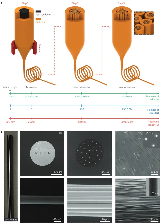
To fabricate nanowires that bridge the macroscopic and the nanoscopic world, we designed a multistep iterative thermal size-reduction process inspired from composite-fibre drawing from polymer reels. We start with a macroscopic polymer rod with an annular hole which is tightly fitted with a thermoelastically compatible material that is to become nanowires on multiple axial elongation and radial reduction. Millimetric fibres obtained from the first thermal size-reduction step are cut and arranged in hexagonal lattices inside a protective jacket, vacuum consolidated and redrawn. This second step reduces the wire size to a few micrometres. The drawing step is repeated a third time with the fibres obtained from the previous step to obtain nanometre-sized wires (Fig. 1, see also Supplementary Fig. S1). Typically, macroscopic rods are reduced by 25- to 300-fold within each step. Using a reduction factor of 50–100 for three iterative steps, a 10 mm initial rod is reduced to hierarchically ordered 10 nm
Semiconductor
Dielectric
Heating
Macroscopic rod
Microwire Nanowire array Nanowire array
10 mm 30¬200 µm 100¬700 nm 5¬50 nm 1 1 500 250,000 200 mm 200 m 100 km 50,000 km Diameter of wire (d) Number of wires (N) Total wire length (L) Ge¬As¬Se¬Te PEI 100 µm 200 µm 100 µm 20 µm 10 µm 10 µm 250 nm 32 nm d = 10 mm
Step 1 Step 2 Step 3
a
b
Figure 1|A new nanofabrication technique, based on iterative size reduction, to produce ordered, indefinitely long nanowire and nanotube arrays.a, A
macroscopic multimaterial rod is reduced to ordered arrays of nanowires by thermal size reduction in a protective polymer matrix in successive steps. Each step starts with structures obtained from a previous step, resulting in geometrical size reduction and increment in wire number and length. Using the technique, we produced millions of kilometre-long nanowires with sub-10 nm diameter and an aspect ratio of 1011. b, As an example, a 10 mm amorphous
semiconducting rod (Ge–As–Se–Te) is reduced to hundreds of metres of single 200 µm wire (reduction factor ×50), ∼30 wires of 5 µm diameter (reduction factor ×50) and ∼1,000 wires of 250 nm (reduction factor ×50). Nanowire arrays are obtained as embedded in a dielectric polyetherimide encapsulation. Wire-array cross-sections with well-ordered wires and extracted, globally oriented slivers are shown after each step. Inset: Transmission electron microscopy image of a single 32-nm-thick nanowire obtained by further scaling down the third-step nanowires.
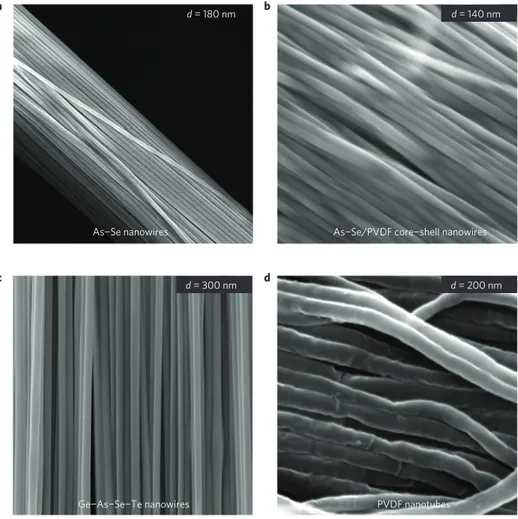
d = 180 nm d = 140 nm
d = 200 nm d = 300 nm
As¬Se nanowires
Ge¬As¬Se¬Te nanowires
As¬Se/PVDF core¬shell nanowires
PVDF nanotubes
a b
c d
Figure 2|Globally ordered, multimaterial nanowire, nanotube and cylindrical core–shell arrays.Nanowire and nanotube arrays are extracted from
polymer matrix by chemical etching, retaining their global alignment. a, As2Se3semiconducting nanowires. b, As2Se3nanowire core with PVDF
encapsulation forming a glass–polymer cylindrical core–shell structure. c, High-refractive-index low-bandgap semiconducting Ge15As25Se15Te45nanowire
slivers. d, Hollow-core piezoelectric polymer (PVDF) nanotube slivers with ∼20 nm wall thickness. Hollow cores of the tubes are evident from the creases in the slivers after extraction by chemical etching.
wires. The total number of nanowires and their ultimate size distribution is determined by the number of packed fibres after each step, the total number of iterative steps and the reduction factor as shown in Fig. 1.
We demonstrate nanowire production using chalcogenide semi-conducting glasses in Fig. 1. Stable glass-making non-oxide chalco-gen compounds have low softening points, making them amenable for thermal co-drawing inside polymer matrices owing to their excellent match of thermomechanical properties (Supplementary Fig. S2). We synthesized a 10-mm-diameter glass-making chalco-genide Ge15As25Se15Te45 (GAST, Tg∼ 190
◦
C) from high-purity elemental constituents using the conventional melt-quenching technique30 (see the Methods section). Around the glass rod, a high-temperature engineering polymer (polyetherimide, Tg∼ 220◦
C) is rolled and thermally consolidated in vacuum. The composite structure is then thermally drawn to reduce radial size (Supplementary Fig. S3). Typically, the process is carried out at 50 cm min−1 drawing speed while feeding the macroscopic rod at 1.5 mm min−1into a furnace at 275◦
C. The ‘fibre wires’ obtained from the first drawing are then packed and vacuum consolidated to prepare a second-step macroscopic rod. Vacuum consolida-tion ensures structural homogeneity and purity from defects that may adversely affect the subsequent thermal drawing process (see the Methods section). Beginning with a 10-mm-diameter GAST rod, the diameter is successively reduced to 200 µm,5 µm and 250 nm within each drawing step. Further reduction in the third
step results in sub-50 nm nanowire arrays. In Fig. 1, we show a perfectly ordered array of GAST micro- and nanowires in the polyetherimide polymer cross-section. It is remarkable that the macroscopic structure is undistorted after the drawing steps. We have also demonstrated that the micro- and nanowires can be extracted from the polymer matrix retaining their global align-ment simply by exposing the polymer section to organic etching agents (dichloromethane (DCM) or dimethylacetamide; see the Methods section). Resulting free-standing micro- and nanowire slivers are shown in Fig. 1.
We fabricated a variety of multimaterial nanowire and nanotube structures by using the same technique (Fig. 2; Supplementary Figs S4–S7). Regular nanowire arrays are fabricated from the highly nonlinear glass As2Se3 (Fig. 2a), ordered core–shell arrays of As2Se3–PVDF (polyvinylidene fluoride; Fig. 2b), high-refractive-index GAST glass (Fig. 2c), and photoconductive and phase-change Se glass (Supplementary Figs S4–S6). Separately, nanotubes of piezoelectric PVDF (melting temperature Tm = 171◦C) are obtained using the same process by using PVDF sheets as the filling material and polysulphone (PSU, Tg∼ 190◦C) as the jacket layer (Fig. 2d). PVDF sheets take their tubular shape through melting at the drawing temperature (Tdraw = 240◦C) followed by self-organization due to high surface energy between the fluoride polymer and the protective PSU jacket. Macroscopic PVDF tubes can be seen after the first and second step drawings, and more interestingly tubular shapes are conserved in the
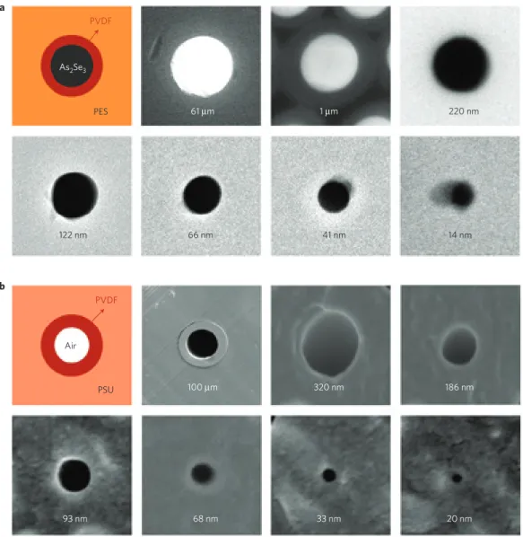
PVDF PVDF PES As2Se3 100 µm 320 nm 61 µm 1 µm 220 nm 186 nm 33 nm 20 nm 93 nm 68 nm 122 nm 66 nm 41 nm 14 nm Air PSU a b
Figure 3|Regular size reduction and ultimate achievable limit with multimaterial iterative size-reduction technique.We produced kilometre-long nanowires and nanotubes with any diameters within the 100 µm–10 nm range by preserving ordered geometry. a, As2Se3–PVDF core–shell nanowires
scaled regularly from 200 µm to 14 nm. b, Hollow-core PVDF nanotubes scaled regularly from 200 µm to 20 nm without losing structural integrity. Smearing around the nanowires is caused during sample preparation with ultramicrotomy.
nanoscale, resulting in very long arrays of nanofluidic channels in a flexible polymer fibre. Thermal melt-drawing of globally aligned PVDF nanotubes is an interesting alternative to existing templating and sol–gel methods for producing high-density nanotube channels31.
Nanowire fabrication with low-melting-temperature metals and metal alloys (Sn, SnPb, SnAg) was also explored using the same process. Fibre drawing is ideally designed for glassy materials; however, if it is possible to melt the crystalline substance without oxidizing inside a protective glassy matrix during thermal draw, crystalline rods will melt and recrystallize as elongated wires conserving the structural integrity21,22,30. Recently, it was shown that other phases (such as metals and semimetals) can be drawn in an encapsulating glassy matrix32. Here, drawing occurs in a regime dominated by viscous forces, allowing for internal low-viscosity metallic domains to be arranged in cross-sections confined by viscous glassy boundary layers. However, this latter type of composite drawing becomes especially challenging with submicrometre filament sizes. The Taylor process, other attempts and the authors’ own previous work suggests that crystalline materials can be co-drawn in glassy matrices when the drawing conditions are just right. To demonstrate that it is indeed feasible to
fabricate ordered arrays of micrometre- and sub-micrometre-scale metallic wires in polymer fibres, we selected tin and tin alloys owing to their low melting temperature (Tm = 223◦C). The drawing process is carried out with similar parameters to those of chalcogenide glasses. We started with a 1.6-mm-diameter soldering alloy Sn96.5Ag3.5 tightly fitted inside a hollow-core polyethersulphone rod, and scaled successively to 60 and 4 µm (Supplementary Fig. S7).
We demonstrate the utility of the top-down size-reduction technique by producing wires with sizes spanning the whole micro-and nanoscale (Fig. 3). Beginning with the same macroscopic rod, structures of six orders of magnitude in size can be obtained. We demonstrate this facility with core–shell As2Se3–PVDF nanowires and hollow-core PVDF tubes. As2Se3–PVDF core–shell nanowires were regularly scaled down to 61 µm, 1 µm, 220, 122, 66, 41 and 14 nm (Fig. 3a). Hollow-core PVDF nanotubes were scaled regularly, conserving their structural integrity, from 100 µm down to 20 nm (Fig. 3b). It is remarkable that we produce extended lengths of micro- and nanotubes that are highly sought materials in micro- and nanofluidics research. The wires and tubes are obtained as ordered arrays in the surrounding polymer matrix. In the micrographs, smearing around the nanowires is caused during
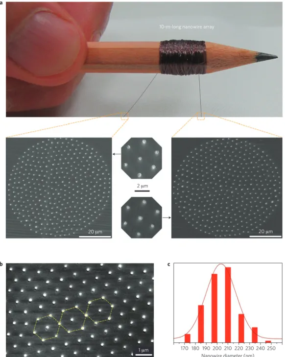
10-m-long nanowire array 2 µm 20 µm 20 µm 1 µm 170 180 190 200 210 220 230 240 250 Nanowire diameter (nm) a b c
Figure 4|Radial and axial uniformity of the nanowire arrays.a, A polymer-embedded nanowire array rolled around a pencil truly spans macroscopic and
nanoscale worlds. Cross-sectional SEM micrographs from both sides of a 10-m-long polymer fibre that contains hundreds of As2Se3–PVDF core–shell
nanowires prove that nanowire arrays are axially uniform to less than 1% for macroscopic distances. b, High-precision hexagonal packing of core–shell nanowires in the polymer matrix. c, Radial size distribution of the nanowires, shown as a histogram, is uniform with a standard deviation of 6.5%. sample preparation with microtomy, making it challenging to
image embedded nanowires in the polymer matrix. For glassy filling materials, the ultimate size reduction limit depends on the drawing dynamics and viscoelastic properties of the matrix. Amorphous glasses and polymers that soften during drawing can be easily reduced to 10 nm radial size without axial breakdown. We infer that, with feed-in and draw speeds tuned and controlled carefully, the drawing process can yield molecular wires; the ultimate size reduction limit is still an enticing question.
We demonstrated radial and axial uniformity of the As2Se3– PVDF core–shell nanowires by taking cross-sectional scanning electron microscopy (SEM) images (FEI, Nova NanoSEM 600) from both sides of a 10-m-long nanowire-embedded fibre, rolled
conveniently on a pencil (Fig. 4). It is extraordinary that the conformal surface coverage of a macroscopic object with nanowires can be achieved trivially. Roughly 400 of the As2Se3–PVDF core–shell nanowires with 200 nm diameter are obtained with two-step iterative drawing. The two-dimensional array structure and integrity of the embedded nanowire arrays are retained for macroscopic lengths. The size distribution along the fibre length is uniform within 1% (Fig. 4a). High-precision hexagonal packing of core–shell nanowires in the matrix is shown in Fig. 4b. The size distribution of the nanowires from the second step is shown as a histogram and found to be uniform within 6.5% (Fig. 4c).
Finally, we investigated the size-dependent photoconductivity of selenium micro- and nanowire arrays fabricated using the described
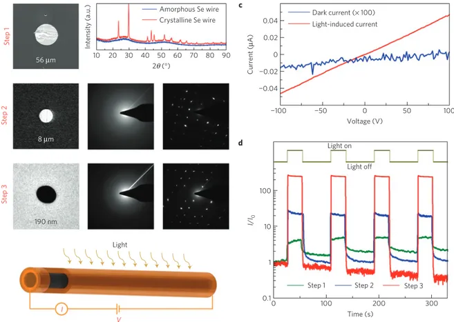
10 20 30 40 50 60 70 80 90 2 (°) Intensity (a.u.) Amorphous Se wire Crystalline Se wire 56 μm 8 μm 190 nm Step 1 Step 2 Step 3 V I Light ¬100 ¬50 0 Light on Light off 0 100 200 300 50 100 Voltage (V) ¬0.04 ¬0.02 0 Current ( μ A) 0.02
0.04 Light-induced currentDark current (× 100)
Time (s)
Step 1 Step 2 Step 3 0.1 1 10 100 I/ I0 a c d b θ
Figure 5|Photoconductivity of selenium microwire and nanowire arrays.a, Amorphous selenium wires are crystallized through heat treatment or by
exposing to the organic reagent pyridine. SEM images of regularly scaled-down individual selenium wires. The electrically conductive hexagonal crystallographic phase is obtained by X-ray and electron diffraction. b, A schematic representation of the photoconductance measurement geometry.
c, The photoconductance from a selenium nanowire in the dark and on white-light illumination. d, A logarithmic increase in the ratio of photocurrent versus
dark current (I/I0) and a reduction in switching time (τ) with reducing nanowire diameter are observed. The performance increase is attributed to the high
optical density of selenium, increased surface-area-to-volume ratio and enhanced scattering in the polymer matrix. technique. Elemental selenium has phase-dependent electrical
conductivity and photoconductivity properties, making it suitable for phase-change memory, optoelectronics and photodetection applications. In a three-step drawing process, we obtained a 56 µm wire, an array of 100 × 8 µm wires and an array of 10,000 × 190 nm nanowires. The structure of the nanowires inside the polyethersulphone polymer matrix is conserved after the drawing steps (Fig. 5). The uniformities of the selenium nanowires from the second and third steps are found to be ±3% and ±11% respectively (Supplementary Fig. S5). Factors contributing to the overall size distribution are slight variations in the fibres that are used to make the macroscopic composite, and the total accumulated size variation from each previous step. Amorphous selenium wires are obtained after drawing, as revealed by X-ray diffraction and transmission electron microscope diffraction (FEI, Tecnai G2 F30). The wires are crystallized through heat treatment, by annealing above the crystallization (Tx= 110◦C) but below the melting temperature27,33and by exposing to the organic reagent pyridine (Fig. 5a, see Methods section). After crystallization we observe that the conductivity increases to 10−4S cm−1 consistent with bulk selenium conductivities34. Electrical measurements were carried out with nanowire arrays by cleaving fibre ends with a razor blade and electrical contacting was achieved using silver paint on the facets of the fibre. Step 3 nanowires were chemically crystallized after extraction from the polymer matrix. Electrical gain due to photoconductivity is measured by shining white light (50 W) while applying voltage bias (Fig. 5b). Step-3 wires make Ohmic contact and feature photoconductivity after
crystallization (Fig. 5c). The photoconductance of the nanowires is observed to be a function of the nanowire number and size in the array. We observed that the I/I0 gain (photocurrent versus dark current) was an order of magnitude larger for step-2 wires and two orders of magnitude larger for step-3 wires with respect to the single selenium microwire from the first drawing (Fig. 5d). The switching between on/off states is also faster with the smaller nanowire sizes. We attribute the logarithmic increase in photoconductance to the high absorption of selenium, increased surface-area-to-volume ratio and enhanced scattering of the incoming beam.
We have demonstrated a unique, high-throughput, lithography-free nanofabrication method to produce macroscopically large nanowire and nanotube arrays. The nanostructures are indefinitely long, ordered, uniform, high-density arrays embedded in a flexible polymer fibre matrix. Diverse multimaterial sets and disparate com-binations are used to obtain crystalline semiconducting nanowire arrays, chalcogenide nanowire array waveguides, piezoelectric poly-mer nanotubes and cylindrical core–shell structures. It is an open question if molecular wires can be obtained using the method. The ultimate size reduction for the nanowires needs to be studied by optimizing drawing parameters for thermoviscous materials and materials that melt during drawing separately. On the other hand, the material set can also be widened to include semiconductors, such as Si and Ge, that soften/melt at higher temperatures using suitable glassy matrices.
We expect that a whole new family of radically novel nanowire applications will be enabled owing to the unique
geometry and material set used. We identify a number of enticing applications that are of current and rigorous scientific and technical interest. For example, these nanostructures can be exploited in nanowire electronics, as large-area conformal photodetectors, large-area flexible nanowire sensors15, scalable high-density nanowire-based phase-change memory35,36 and in high-speed reconfigurable field-effect transistors33; in energy harvesting, large-area cylindrical heterostructure nanowires can be used as active cells37,38but also for passive light enhancement in resonance-enhanced third-generation photovoltaics39,40; in semiconductor nanophotonics, polymer-embedded chalcogenide nanowires can be used as high-refractive-index dielectric structures for size-dependent absorption41, structural colouring42 and biomimicry, and as dielectric metamaterials43; in nonlinear photonics, ordered nanowires can be used as high-power zero-dispersion optical arrays for new frequency generation44and in discrete optics45; in mechanics, nanowire-embedded high-strength composites29; in acoustics, flexible piezoelectric nanowires and nanotubes can be used as sensors and actuators46, as pumps, in energy harvesting47 and as nanochannels in nanofluidics.
Methods
Synthesis of chalcogenide-glass rods. As2Se3and Se rods, 10 mm in diameter
and 15 cm in length, are prepared by melting commercially bought glasses (Amorphous Materials) and pellets (Alfa Aesar) in a vacuum-sealed quartz tube followed by water quenching. Ge15As25Se15Te45glass rods (the same diameter)
are prepared from high-purity elements (Alfa Aesar) using the sealed-ampoule melt-quenching technique. The weighted materials are placed in a quartz tube under nitrogen atmosphere in a glove box (H2O, O2below 0.1 ppm). The quartz
tube is kept at 330◦C for an hour under vacuum to remove surface oxides and
sealed (10−6torr). The sealed ampoule is then heated to 950◦C, rocked for 18 h and
then quenched in iced water.
Macroscopic-composite preparation, consolidation and thermal size reduction.
Macroscopic rods that will undergo axial elongation and radial size reduction are structures approximately 30 mm in diameter. These structures are prepared in a clean pressure flow room, by tightly rolling polyethersulphone or polyetherimide films around chalcogenide glass rods (10 mm diameter) until the diameter is 30 mm (see Supplementary Fig. S1). Then, the macroscopic structure is thermally consolidated under vacuum (10−3torr), above the glass transition temperature
of the polymer and glasses to fuse (260◦C for 30 min). Step-2 and higher-step
structures are prepared with previously obtained polymer–wire fibres and a hollow-core polymer rod fabricated by rolling polymer sheets on a Teflon rod, consolidation and removing the Teflon rod. About 100 fibres with 0.5 mm diameters are cut as 10 cm fibres, tightly packed and placed inside the hollow-core polymer rod. The structure is consolidated once more to fuse packed fibres to the outer polymer jacket (250◦C for 15 min). The second consolidation step ensures
structural integrity during drawing. The macroscopic structure is heated and drawn into hundreds of metres of micro- and nanowire in a vertical two-zone furnace, with a top-zone temperature of 275◦C and bottom zone 200◦C (see
Supplementary Fig. S3). The nanowire diameter is controlled using a laser micrometer by monitoring the fibre diameter.
Nanowire and nanotube extraction. The polymer encapsulating the nanowires
and nanotubes was extracted for electron microscopy imaging in the longitudinal dimension by DCM (Carlo Erba). Nanowire or nanotube arrays embedded in polymer were fixed on a glass substrate by means of aluminium foil, and then half soaked in bottles containing DCM. The extracted nanostructures were further rinsed gently with DCM to remove residual polymer. A final O2plasma treatment
(Nanoplas DSB6000) for several hours was applied for chalcogenide and metal nanowires to remove organic residues.
Nanowire crystallization by thermal and chemical methods. Step-1 selenium
nanowires were crystallized by annealing at 150◦C for 1 h. Step-2 nanowire
crystallization occurred after keeping nanowire arrays at 220◦C for 15 min and
cooling to room temperature in 1.5 h. For crystallization of step-3 selenium nanowire arrays, extracted nanowire arrays were soaked overnight in a 10% pyridine (Riedel-de Haën) solution in isopropanol.
Received 8 January 2011; accepted 28 April 2011; published online 12 June 2011; corrected after print 19 July 2011
References
1. Lu, W. & Lieber, C. M. Nanoelectronics from the bottom up. Nature Mater. 6, 841–850 (2007).
2. Thelander, C. et al. Nanowire-based one-dimensional electronics. Mater. Today
9, 28–35 (October, 2006).
3. Tian, B., Xie, P., Kempa, T. J., Bell, D. C. & Lieber, C. M. Single crystalline kinked semiconductor nanowire superstructures. Nature Nanotech. 4, 824–829 (2009).
4. Caroff, P., Dick, K. A., Johansson, J., Messing, M. E., Deppert, K. & Samuelson, L. Controlled polytypic and twin-plane superlattices in III–V nanowires. Nature Nanotech. 4, 50–55 (2009).
5. Li, Y., Qian, F., Xiang, J. & Lieber, C. M. Nanowire electronic and optoelectronic devices. Mater. Today 9, 18–27 (October, 2006).
6. Freer, E. M. et al. High-yield self-limiting single-nanowire assembly with dielectrophoresis. Nature Nanotech. 5, 525–530 (2010).
7. Takei, K. et al. Nanowire active matrix circuitry for low-voltage macro-scale artificial skin. Nature Mater. 9, 821–826 (2010).
8. Yan, R., Gargas, D. & Yang, P. Nanowire photonics. Nature Photon. 3, 569–576 (2009).
9. Yang, P., Yan, R. & Fardy, M. Semiconductor nanowire: What’s next?
Nano Lett.10, 1529–1536 (2010).
10. Lieber, C. M. & Wang, Z. H. Functional nanowires. MRS Bull. 32, 99–104 (2007).
11. Smith, P. A. et al. Electric-field assisted assembly and alignment of metallic nanowires. Appl. Phys. Lett. 77, 1399–1401 (2000).
12. Jamshidi, A. et al. Dynamic manipulation and separation of individual semiconducting and metallic nanowires. Nature Photon. 2, 85–89 (2008).
13. Huang, Y., Duan, X. F., Wei, Q. Q. & Lieber, C. M. Directed assembly of one-dimensional nanostructures into functional networks. Science 291, 630–633 (2001).
14. Ahn, J-H. et al. Heterogeneous three-dimensional electronics by use of printed semiconductor nanomaterials. Science 314, 1754–1757 (2006).
15. Park, W. I. et al. Controlled synthesis of millimeter-long silicon nanowires with uniform electronic properties. Nano Lett. 8, 3004–3009 (2008).
16. Sazio, P. J. A. et al. Microstructured optical fibers as high-pressure microfluidic reactors. Science 311, 1583–1586 (2006).
17. Suryavanshi, A. P., Hu, J. & Yu, M. F. Meniscus-controlled continuous fabrication of arrays and rolls of extremely long micro- and nano-fibers.
Adv. Mater.20, 793–796 (2008).
18. Martensson, T. et al. Fabrication of individually seeded nanowire arrays by vapour–liquid–solid growth. Nanotechnology 14, 1255–1258 (2003). 19. McAlpine, M. C., Ahmad, H., Wang, D. W. & Heath, J. R. Highly ordered
nanowire arrays on plastic substrates for ultrasensitive flexible chemical sensors.
Nature Mater.6, 379–384 (2007).
20. Russell, P. Photonic crystal fibers. Science 299, 358–362 (2003). 21. Bayindir, M. et al. Metal–insulator–semiconductor optoelectronic fibres.
Nature431, 826–829 (2004).
22. Abouraddy, A. F. et al. Towards multimaterial multifunctional fibres that see, hear, sense and communicate. Nature Mater. 6, 336–347 (2007).
23. Bayindir, M. et al. Kilometer-long ordered nanophotonic devices by preform-to-fiber fabrication. IEEE J. Sel. Quant. Electron. 12, 1202–1213 (2006). 24. Yildirim, A., Vural, M., Yaman, M. & Bayindir, M. Bio-inspired optoelectronic
nose with nanostructured wavelength scalable hollow-core infrared fibers.
Adv. Mater.22, 1263 (2011).
25. Tong, L. M. et al. Subwavelength-diameter silica wires for low-loss optical wave guiding. Nature 426, 816–819 (2003).
26. Zhang, X. J., Ma, Z. Y., Yuan, Z. Y. & Su, M. Mass-productions of vertically aligned extremely long metallic micro/nanowires using fiber drawing nanomanufacturing. Adv. Mater. 20, 1310–1314 (2008).
27. Deng, D. S. et al. Processing and properties of centimeter-long, in-fiber, crystalline-selenium filaments. Appl. Phys. Lett. 96, 023102 (2010). 28. Deng, D. S. et al. In-fiber semiconductor filament arrays. Nano Lett. 8,
4265–4269 (2008).
29. Donald, I. W. Production, properties and applications of microwire and related products. J. Mater. Science 22, 2661–2679 (1987).
30. Bayindir, M. et al. Thermal-sensing fiber devices by multimaterial codrawing.
Adv. Mater.18, 845–849 (2006).
31. Sun, C. L. et al. Fabrication and characterization of Ni/P(VDF-TrFE) nanoscaled coaxial cables. Appl. Phys. Lett. 90, 253107 (2007).
32. Tyagi, H. K. et al. Plasmon resonances on gold nanowires directly drawn in a step-index fiber. Opt. Lett 35, 2573–2575 (2010).
33. Danto, S. et al. Fibre field-effect device via in situ channel crystallization.
Adv. Mat.22, 4162–4166 (2010).
34. Keck, P. A. Photoconductivity in vacuum coated selenium films. J. Opt. Soc. Am.
42, 221–224 (1952).
35. Lee, S. H. et al. Highly-scalable nonvolatile and ultra-low power phase-change nanowire memory. Nature Nanotech. 2, 626–630 (2007).
36. Yu, B. et al. Chalcogenide-nanowire-based phase change memory.
IEEE Trans. Nanotech.7, 496–502 (2008).
37. Tian, B. et al. Coaxial silicon nanowires as solar cells and nanoelectronic power sources. Nature 449, 885–889 (2007).
38. Kelzenberg, M. D. et al. Enhanced absorption and carrier collection in Si wire arrays for photovoltaic applications. Nature Mater. 9, 239–244 (2010).
39. Cao, L. et al. Semiconductor nanowire optical antenna solar absorbers.
Nano Lett.10, 439–445 (2010).
40. Grandidier, J., Callahan, D. M., Munday, J. N. & Atwater, H. A. Light absorption enhancement in thin-film solar cells using whispering gallery modes in dielectric nanospheres. Adv. Mater. 23, 1272–1276 (2011). 41. Cao, L. et al. Engineering light absorption in semiconductor nanowire devices.
Nature Mater.8, 643–647 (2009).
42. Cao, L. et al. Tuning the color of silicon nanostructures. Nano Lett. 10, 2649–2654 (2010).
43. Vynck, K. et al. All-dielectric rod-type metamaterials at optical frequencies.
Phys. Rev. Lett.102, 133901 (2009).
44. Eggleton, B. J. et al. Chalcogenide photonics. Nature Photon. 5, 141–148 (2011). 45. Minardi, S. et al. Three-dimensional light bullets in arrays of waveguides.
Phys. Rev. Lett.105, 263901 (2010).
46. Egusa, S. et al. Multimaterial piezoelectric fibres. Nature Mater. 9, 643–648 (2010).
47. Chang, C. et al. Direct-write piezoelectric polymeric nanogenerator with high energy conversion efficiency. Nano Lett. 10, 726–731 (2010).
Acknowledgements
This work was partially supported by the State Planning Organization (DPT) and TUBITAK under project No 106G090. M.B. acknowledges support from the Turkish Academy of Sciences Distinguished Young Scientist Award (TUBA GEBIP).
Author contributions
M.Y. and M.B. designed and carried out research, analysed data and wrote the paper. M.K., T.K., M.Y., and M.B. carried out fabrication of nanowires and nanotubes. E.O. and O.A. made photoconduction measurements, E.O.O. and H.D. took SEM and transmission electron microscope micrographs and E.K. and M.B. drew schematic representations.
Additional information
The authors declare no competing financial interests. Supplementary information accompanies this paper on www.nature.com/naturematerials.Reprints and permissions information is available online at http://www.nature.com/reprints. Correspondence and requests for materials should be addressed to M.B.
In the version of this Letter previously published, the key for Fig. 5c was incorrect. This error has now been corrected in the HTML and PDF versions.