A New Simulation Model for Inhomogeneous Au/
n-GaN Structure
1Nese Kavasoglu, Abdulkadir Sertap Kavasoglu, and Bengul Metin
Mugla Sitki Kocman University, Faculty of Sciences, Department of Physics, Photovoltaic Material and Device Laboratory, 48000 Mugla, Turkey
Mugla Sitki Kocman University, Faculty of Sciences, Department of Physics, Solid State Electronics Laboratory, 48000 Mugla, Turkey
e-mail: [email protected]
Submitted April 10, 2015; in final form, November 12, 2015
Abstract—The larger the device area, the more difficult to carry on homogeneity during the fabrication and following treatments. Structural inhomogeneity may indicate themselves in variations in local electronic device parameters. Electrical current through the potential barriers is exponentially sensitive to the local device parameters and its f luctuations in the Schottky devices. A new simulation program is developed to describe a relation between multiple, random barrier heights and current-voltage characteristics of the Schottky device. We model the barrier height inhomogeneity in terms of random microcells connected in parallel, which have different barrier height values. Analyzing the integral of the simulated light current-volt-age curves show that f luctuations of the local barrier height result in a degradation of the open circuit voltcurrent-volt-age, fill factor and in consequence, of the over all power conversation efficiency. The implementation described here is quite general and can be used to simulate any device parameter f luctuations in the Schottky devices. DOI: 10.1134/S1063782616050134
1. INTRODUCTION
Number of physical problems depend on the inho-mogeneity arise from large area thin film device fabri-cation processes. Numerical modeling of devices is a realistic approximation for exploration of device behaviors. An equivalent circuit model consisting of parallel connected diodes with different electronic quality simulates the electronic properties of the inho-mogeneous device. In this study, we examined the effects of the local barrier height variations on the light current voltage (I–V) characteristics, open circuit voltage, and fill factor. Simulation program has been developed and operated for the Au/n-GaN device structure. GaN is a wide bandgap material (3.4 eV) and it is the most promising material for the fabrica-tion of light emitting diodes, lasers, detectors, photo-voltaic energy conversation, fiber optic communica-tion, high-temperature, highpower and high-fre-quency transistors applications due to its direct bandgap [1–3].
Randomly distributed dopand atoms within the semiconductor, atomic steps and lattice defects at the interface, the relative orientation of semiconductor and metal atoms, grain boundaries in the metal, inter-face roughness bring on laterally varying Schottky bar-riers [4–12]. Nonuniform interfacial on a semicon-ductor leads to parallel contacts between metal and semiconductor. Penetration of metal through semi-conductor makes localized contacts to semisemi-conductor.
Maffeis et al. reports evidence of Au–GaN intermix-ing regions at Au/GaN interface [13]. Also, they viewed this layer by TEM. This layer consists of Au grains embedded in a GaN matrix. The complex inter-face brings about the abnormal diodic properties. Understanding the electrical characteristics of these devices naturally induces a number of challenges. Very little is known about the characteristics of devices with parallel contacts and new studies should be conducted to clarify the issue. Direct images of Schottky barrier height f luctuations in the devices have been obtained using ballistic electron emission spectroscopy and researchers correlated them with a Gaussian distribu-tion funcdistribu-tion. Simuladistribu-tion studies for investigadistribu-tion of the effect of the Gaussian distribution of the barrier heights on the current voltage characteristics had been reported in the literature [14–18].
Computer simulations have become a convenient part of mathematical modeling of many devices for optoelectronic applications. One can analyze, design and operate complex systems by simulation. A simula-tion model mimics to algorithms and equasimula-tions used to represent the behavior of the device being modeled. The suitable handling of inhomogeneity effects is nec-essary both for calculating accurate current voltage characteristics and the study of lateral inhomogene-ities with numerical simulations [19, 20]. Numerical modeling and simulation of devices are useful for developing the newer technologies and the low priced methods to test device operations and optimizations. A proper understanding of the device characterization
1The article is published in the original.
SEMICONDUCTOR STRUCTURES, LOW-DIMENSIONAL SYSTEMS,
AND QUANTUM PHENOMENA
is crucial since it is a powerful tool to calculate the physical and electronic parameters of a device. Mod-eling enables us to see how a real world performance of the devices will fulfill under different conditions. In the meantime, understanding the nature of inho-mogeneity effect on the device performance will be a vital endeavor in the near future for improvement of Au/n-GaN devices or other devices.
In this study, the key parameter is the characteristic barrier height f luctuations in the device. Device was assumed to have inhomogeneous barrier height and changes in barrier heights of microcells were consid-ered to be random. Current depends exponentially on the value of the Schottky barrier height. Barrier height f luctuating effect on the I–V characteristics of the Au/n-GaN device has been studied by developed sim-ulation software using more general fundamental semiconductor device equations. During the simula-tion process, Au/n-GaN device is interpreted based on the existence of the barrier height inhomogeneities.
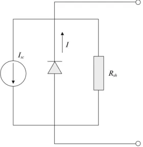
2. METHOD OF NUMERICAL SIMULATION We simulate the current voltage characteristics of inhomogeneous device by connecting different micro-cells in parallel. The current voltage characteristic of a single element, which is shown in Fig. 1, is represented by Shockley equation [21]. (1) ⎡ Φ ⎤ ⎡ ⎛ ⎞ ⎤ = ⎢− ⎥ ⎢ ⎜ ⎟− ⎥ ⎣ ⎦ ⎣ ⎝ ⎠ ⎦ + − 2 B B ( ) * exp exp 1 , bo sc sh q q I V AA T V k T nk T V I R
where A is the diode area, A* is the effective
Richard-son constant, T—temperature, Φbo—barrier height,
kB—Boltzmann constant, q—the electron charge, n— the diode factor, Rsh—shunt is resistance, Isc—the light generated current.
Actually, inhomogeneities in the device are unavoidable and are present invariably even in the most carefully fabricated system. When modeling dif-ferent kinds of junctions, a single exponential Shock-ley equation is not enough to display variations of sev-eral electrical parameters in the device. In this study, electronic properties of the inhomogeneous device are simulated by connecting different microcells in paral-lel, such as one shown in Fig. 1. The system is consid-ered to have a number of non-interacting microcells with each corresponding to a different barrier height within the distribution limit. The current voltage char-acteristic of a microcell is exponential, because of this microcells can be exponentially sensitive to small vari-ations in the local device parameters. The current is assumed to be a sum of the currents following in all the individual microcells. The simulation studies per-formed on Au/n-GaN device assume one constant series resistance for all microcells.
The barrier height control and distribution in the device is very important in determining the perfor-mance of devices such as diodes and transistors. Our main goal is to investigate barrier height inhomogene-ity effect on electrical characteristics by developed simulation program. The illuminated current-voltage characteristics for 0.4 × 0.4 cm2 area of Au/n-GaN
device are obtained from developed simulation pro-gram. Microcells are assumed to be square in shape. The device is sliced into 40 by 40 microcells to cover an area 100 μm2 each. Total cell number in the device is
1600. Each microcell represents a discrete circuit unit under light as seen in Fig. 1. Any deviation of a micro-cell parameter from the rest of the micromicro-cells would indicate inhomogeneity.
Barrier height of each microcell to be different from each other is introduced to program in accordance with the following formula:
, (2) where j is the cell number, ϕb0(0) is the zero bias bar-rier height offset value, Γ is the barbar-rier height f luctua-tion factor, RND is the random generated number var-ies between 0 and 1. The distribution pattern of barrier height is characterized by Γ, which is percentage devi-ation from the zero bias barrier height offset value. ϕb0(0) value is introduced from experimental studies
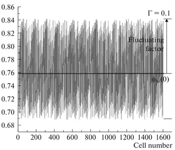
[22]. Random distribution of zero barrier height in the device is shown in Fig. 2. Gamma (Γ) is a measure of inhomogeneity. Inhomogeneity is introduced to pro-gram via f luctuation factor term whereby barrier height of each microcell is different from each other’s represents inhomogeneity. Barrier height variation from first cell to final cell in the device has been suc-cessfully used for inhomogeneous device modeling.
Φbo j, = φbo(0)+ Γφ( b0(0))(2RND−1)
Fig. 1. Equivalent circuit elements consist of a current
source Isc, a parallel resistance Rsh and a diode with current I.
For simulation purposes, the device is divided j microcells. Each microcell represents a discrete circuit unit.
I Isc
During the studies, other than the barrier height of the device parameters were kept constant.
Our developed simulation program runs as given below lines:
Input endpoints Vmin, Vmax and positive integer n
(number of data). Input cell number.
Step 1: Input the offset value (Φbo(0)).
Step 2: Input the f luctuating factor of barrier height.
Step 3: Barrier height values of each microcell were f luctuated around constant value according to Eq. (2) for j = 1 to cell number. Perform the simulation and barrier height values for each microcell.
Step 4: Next j.
Step 5: For V = Vmin to Vmax step dV. Step 6: For i = 1 to cell number do step 7.
Step 7: The total current through the device is cal-culating by simply adding the individual current through each microcell using electronic device param-eters:
Step 8: Next i.
Step 9: Next V, where Rs is the series resistance.
The suggestion is that there are a number of parallel microcells of different barrier heights, each contribut-ing the current individually. The device is modeled in the presence of a parasitic resistance for all microcells and individual shunt resistances of microcells by the
cell number 0 2 B 1 B * exp exp ( ) 1 . b j j s s sc j j sh j q I AA T k T V IR q V IR I n k T R = − Φ ⎛ ⎡ ⎤ = ⎜ ⎢ ⎥ ⎝ ⎣ ⎦ ⎞ ⎡ ⎛ ⎞ ⎤ − ×⎢ ⎜ − ⎟− +⎥ − ⎟⎟ ⎣ ⎝ ⎠ ⎦ ⎠
∑
summation of multi exponential expressions, plus resistive shunt terms and minus light generated current terms. We have evaluated simulation program to inves-tigate dependence of I–V characteristics on barrier
height f luctuations in the device. Simulation data pre-sented in this study deals with AM0 solar spectrum and at room temperature.
3. RESULTS AND DISCUSSION
In this study, rigorous numerical calculation of illu-minated current voltage characteristics were carried out by using a simulation program developed by our group for an Au/n-GaN device structure. The system is considered to have a number of non-interacting par-allel microcells with each corresponding to a different, random barrier height within the distribution limit.
1600 regions of increasing or decreasing barrier height enforce alternations in the barrier height in the Au/n-GaN device. Barrier height values are random-ized around the barrier height offset value. The ran-domness of the barrier height values has been tested with chisquare test.
The magnitude of the barrier height is determined by f luctuation factor.
Inhomogeneities in the device can be characterized in terms of the local values of the barrier height. Figure 3 shows an example of the local barrier height variation in the Au/n-GaN device.
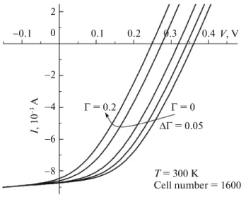
Current voltage characteristics of the Au/n-GaN device are simulated for room temperature and differ-ent barrier height f luctuating factor values. Figure 4 represents the illuminated current voltage characteris-tics of the Au/n-GaN device. It is quite clear that the illuminated current voltage characteristics are sensi-tive to the barrier height f luctuating factor.
One of the difficulties for the improvement of effi-ciency in optoelectronic devices is relatively low Voc
(open circuit voltage). Figure 4 shows barrier height f luctuating factor dependent illuminated current volt-age characteristics of Au/n-GaN device. The barrier
Fig. 2. Fluctuation of barrier height around a constant
value from first cell to final cell. 0.86 φbo(V) 0.84 0.82 0.80 0.78 0.76 0.74 0.72 0.70 0.68 1600 Cell number 1400 1200 1000 800 600 400 200 0 φbo(0) Fluctuating factor Γ = 0.1
Fig. 3. An example of randomized f luctuations in the
bar-rier height of the Au/n-GaN device. In this case f luctua-tion factor is 0.1. φbo (eV) 0.84 0.82 0.80 0.78 0.76 0.74 0.72 0.70 y, μm 0 0 0.9 0.8 0.7 1000 2000 2000 3000 3000 4000 1000 x, μm
height f luctuating factor primarily affects to the Voc.
Simulation results clearly display that when the inho-mogeinity increases Voc decreases as reported by Malm
et al. [23].
With the help of one diode model equation under light (with Rs = 0 and Rsh = ∞ and neglecting the one
in the diode law), it is obtained Eq. (3) for homogeny device [21]:
(3) If there is inhomogeneities in the device, Eq. (3) is represented as Eq. (4):
(4) where Voc and are the open circuit voltage of
inho-mogeneous and hoinho-mogeneous device, respectively; ∋ term stems from inhomogeneities in the device.
The reverse saturation current is given by:
(5) Φbo ≈ 2Eg/3 is for the depletion contact formed on
n-type substrate (Eg is the band gap energy).
Conse-quently, f luctuations of barrier height means band gap inhomogeneity in the device hence result in ∋ in Eq. (4). Band gap of the materials is affected by growth techniques. Band gap engineering is the process of controlling or altering the band gap of a material by controlling the composition of certain semiconductor alloys. The motivation for the materials growths is to produce suitable band gap materials for use in
opto-⎛ ⎞ = − ⎜ ⎟ ⎝ ⎠ 2 0 B * log . g oc sc E k T AA T V q q I = 0− , oc oc V V ] 0 oc V ⎛ Φ ⎞ = ⎜− ⎟ ⎝ ⎠ 2 0 B * exp q bo . I AA T k T
electronics. Precise control of the composition, thick-ness, uniformity and doping levels is investigated [24]. Several simulation studies have been performed with changing the f luctuation factor values. Our sim-ulation studies show that barrier height f luctuation factor values are very important in optimization of optoelectronic device fill factor and efficiency values. A decrease has been seen in the fill factor and the effi-ciency, with the increasing of barrier height f luctuat-ing factor.
Fluctuations in the barrier height of disordered microstructures due to spatial f luctuations in the microstructure of the device strongly affect current voltage characteristics. For handling optimum device performance, device layers to be uniform in composi-tion with any f luctuacomposi-tions in barrier height must keep to a minimum. It is seen that Voc value of the device is
strongly governed by barrier height f luctuating factor. The barrier height f luctuating factor also affects fill factor, and hence the power loss. Several optoelec-tronic device materials are prepared by different tech-niques. Some of them have gathered much attention as new age device material by reason of simple fabrica-tion process, mass produceability and material econo-mization. Recently, researchers show that high effi-cient optoelectronic devices can be achieved by fabri-cating homogeny device structures. Reports display that key technology to obtain especially high Voc and
fill factor is the grain size and electrically homoge-neous structures. Barrier height f luctuating affects inversely efficiency and fill factor of the device as seen in Fig. 5.
4. CONCLUSION
Device modeling of Au/n-GaN device has been investigated with taking barrier height f luctuating
fac-Fig. 4. The illuminated current voltage characteristics of
the multi diode simulations for variations in the barrier height. 0.1 T = 300 K Cell number = 1600 0.2 0.3 0.4 V, V −0.1 2 0 I, 10 − 3 A −2 −4 −6 −8 Γ = 0 Γ = 0.2 ΔΓ = 0.05
Fig. 5. Barrier height f luctuating factor dependent fill
fac-tor (FF) and efficieny (η).
4 0.44 0.42 0.40 0.38 0.36 0.34 0.32 3 2 1 0 0.05 0.10 0.15 0.20 Γ η , % η FF F.F.
tor into account by simulation. It has been found that barrier height f luctuating factor is of importance for enhancing Voc, efficiency and fill factor. Developed simulation program offers a favorable tool not only for optimum design, but also performance analysis of optoelectronic devices.
It is displayed that a strong correlation between barrier height f luctuating factor and illuminated cur-rent voltage characteristics of Au/n-GaN device. Fluctu-ating factor values have been found to be responsible for the current transport across the Au/n-GaN device with spatial inhomogeneity. As the simulation results of Au/n-GaN device show, Voc, fill factor, and efficiency
considerably follow the barrier height f luctuating fac-tor. The barrier height f luctuation factor is an import-ant parameter that strongly affects the device charac-teristics, which should be taken into account in the realistic simulations. We believe that understanding effects of barrier height inhomogeneity will help to improve device performance and stability.
ACKNOWLEDGMENTS
This work was supported by Mugla Sitki Kocman University Scientific Research Project (SRP) with the project no. 2011/13. The authors wish to express appreciation to Mugla Sitki Kocman University Sci-entific Research Project.
REFERENCES
1. L. S. Yu, Q. Z. Liu, Q. J. Xing, D. J. Qiao, S. S. Lau, and J. Redwing, J. Appl. Phys. 84, 2099 (1998). 2. B. Akkal, Z. Benamara, H. Abid, A. Talbi, and B.
Gru-zza, Mater. Chem. Phys. 85, 27 (2004).
3. C. Touzi, A. Rebey, and B. Eljani, Microelectron. J. 33, 961 (2002).
4. R. T. Tung, Phys. Rev. B 45, 13509 (1992).
5. M. Biber, O. Gullu, S. Forment, R. L. Van Meirhae-ghe, and A. Turut, Semicond. Sci. Tech. 21, 1 (2006).
6. I. M. Afandiyeva, S. Demirezen, and S. Altındal, J. Alloys Comp. 552, 423 (2013).
7. K. S. Kima, R. K. Gupta, G. S. Chung, and F. Yakuph-anoglu, J. Alloys Comp. 509, 10007 (2011).
8. O. Vural, Y. Safak, S. Altındal, and A. Turut, Curr. Appl. Phys. 10, 761 (2010).
9. S. Altındal, H. Kanbur, A. Tataroglu, and M. M. Bul-bul, Physica B 399, 146 (2007).
10. K. Ejderha, N. Yıldırım, B. Abay, and A. Turut, J. Alloys. Compd. 484, 870 (2009).
11. B. Kinaci, S. S. Cetin, A. Bengi, and S. Ozcelik, Mater. Sci. Semicond. Proc. 15, 531 (2012).
12. O. Pakma, N. Serin, T. Serin, and S. Altındal, Physica B 406, 771 (2011).
13. T. G. G. Maffeis, M. C. Simmonds, S. A. Clark, F. Peiro, P. Haines, and P. J. Parbrook, J. Appl. Phys. 92, 3179 (2002).
14. M. Bhaskar Reddy, A. Ashok Kumar, V. Janardhanam, V. Rajagopal Reddy, and P. Narasimha Reddy, Curr. Appl. Phys. 9, 972 (2009).
15. A. D. D. Dwivedi, A. K. Singh, R. Prakash, and P. Chakrabarti, Curr. Appl. Phys. 10, 900 (2010). 16. M. Gokcena, T. Tuncc, S. Altindal, and I. Uslu, Curr.
Appl. Phys. 12, 525 (2012).
17. S. Demirezen and S. Altındal, Curr. Appl. Phys. 10, 1188 (2010).
18. E. Dobrocka and J. Osvald, J. Appl. Phys. Lett. 65, 575 (1994).
19. G. T. Koishiyev and J. R. Sites, Sol. Energy Mater. Solar C 93, 350 (2009).
20. U. Malm and M. Edoff, Sol. Energy Mater. Solar Cells 93, 1066 (2009).
21. S. M. Sze, Physics of Semiconductor Devices, 2nd ed. (Wiley, New Jersey, 1981).
22. S. N. Das and A. K. Pal, Vacuum 81, 834 (2007). 23. U. Malm and M. Edoff, Sol. Energy Mater. Solar Cells
93, 1066 (2009).
24. S. C. Riha, B. A. Parkinson, and A. L. Prieto, J. Am. Chem. Soc. 133, 15272 (2011).