Monolayer honeycomb structures of group-IV elements and III-V binary compounds:
First-principles calculations
H. Şahin,1S. Cahangirov,1M. Topsakal,1E. Bekaroglu,1E. Akturk,1R. T. Senger,2and S. Ciraci1,3,
*
1UNAM-Institute of Materials Science and Nanotechnology, Bilkent University, 06800 Ankara, Turkey 2Department of Physics, Izmir Institute of Technology, 35430 Izmir, Turkey
3Department of Physics, Bilkent University, 06800 Ankara, Turkey
共Received 24 July 2009; revised manuscript received 5 October 2009; published 28 October 2009兲 Using first-principles plane-wave calculations, we investigate two-dimensional共2D兲 honeycomb structure of group-IV elements and their binary compounds as well as the compounds of group III-V elements. Based on structure optimization and phonon-mode calculations, we determine that 22 different honeycomb materials are stable and correspond to local minima on the Born-Oppenheimer surface. We also find that all the binary compounds containing one of the first row elements, B, C, or N have planar stable structures. On the other hand, in the honeycomb structures of Si, Ge, and other binary compounds the alternating atoms of hexagons are buckled since the stability is maintained by puckering. For those honeycomb materials which were found stable, we calculated optimized structures, cohesive energies, phonon modes, electronic-band structures, effec-tive cation and anion charges, and some elastic constants. The band gaps calculated within density functional theory using local density approximation are corrected by GW0method. Si and Ge in honeycomb structure are semimetal and have linear band crossing at the Fermi level which attributes massless Fermion character to charge carriers as in graphene. However, all binary compounds are found to be semiconductor with band gaps depending on the constituent atoms. We present a method to reveal elastic constants of 2D honeycomb structures from the strain energy and calculate the Poisson’s ratio as well as in-plane stiffness values. Prelimi-nary results show that the nearly lattice matched heterostructures of these compounds can offer alternatives for nanoscale electronic devices. Similar to those of the three-dimensional group-IV and group III-V compound semiconductors, one deduces interesting correlations among the calculated properties of present honeycomb structures.
DOI:10.1103/PhysRevB.80.155453 PACS number共s兲: 73.22.⫺f, 61.48.De, 63.22.⫺m, 62.23.Kn
I. INTRODUCTION
Last two decades, nanoscience and emerging nanotech-nologies have been dominated by honeycomb-structured carbon-based materials in different dimensionality, such as fullerenes, single-walled and multiwalled carbon nanotubes, graphene and its ribbons. In particular, graphene, a two-dimensional 共2D兲 honeycomb structure of carbon, has been an active field of research.1 Because of unique symmetry,
electron and hole bands of graphene show linear band cross-ing at the Fermi level2resulting in a massless Dirac
fermion-like behavior of charge carriers. As a result, Klein paradox, an interesting result of quantum electrodynamics was ex-pected to be observed in graphene.3–6 Moreover, it was
shown that half-integer quantization of Hall conductance4,7,8
can be observed in graphene. Unusual electronic and mag-netic properties of graphene, such as high carrier mobility and ambipolar effect, have promised variety of applications. In addition to some early works on crystalline order in planar structures,9,10 possibility of very large one-atom-thick 2D
crystals with intrinsic ripples is reported theoretically11 and experimentally.12Not only extended 2D graphene sheets but
also quasi-one-dimensional共1D兲 graphene ribbons with arm-chair or zigzag edges have shown unusual electronic,13–18
magnetic,19–22and quantum-transport properties.23–26
All these experimental and theoretical studies on graphene created significant interest in one-atom-thick hon-eycomb lattices of other group-IV elements and compounds of III-V and II-VI group elements. Recently, the
boron-nitride共BN兲 honeycomb sheet was reported as a stable ionic monolayer.27 BN has the same planar structure as graphene
with a nearest-neighbor distance of 1.45 Å. However, its ionic character causes a gap opening at the K point. Thus, instead of being a semimetal, BN honeycomb structure is a wide band-gap insulator with an energy gap of 4.64 eV. Soon after its synthesis, several studies on nanosheets28 and nanoribbons29–32 of BN have been reported.
Hexagonal monolayer of zinc oxide 共ZnO兲 is a II-VI metal-oxide analog of graphene and BN. Previously, works on nanostructures of ZnO such as nanosheets,33nanobelts,34
nanotubes,35 nanowires,36 and nanoribbons37 were reported
and recently the synthesis of ZnO bilayer honeycomb struc-ture was also achieved.38 In contrast to graphene, ZnO
nan-oribbons have ferromagnetic order in their ground state due to electronic states at the zigzag edges dominated by oxygen atoms.39,40
Two-dimensional SiC honeycomb sheet is another group-IV binary compound displaying interesting properties. While the infinite periodic 2D form of SiC is a semiconduc-tor with 2.55 eV band gap, and its zigzag nanoribbons are magnetic metals, the armchair ribbons are nonmagnetic semiconductors.41 Half metallicity is also predicted for
nar-row SiC zigzag nanoribbons without any chemical decora-tion or applied external field. Furthermore, funcdecora-tionalizadecora-tion of SiC single sheets upon formation of various types of va-cancies and adatom decoration was also predicted.42
Very recently, we have reported that among group-IV el-ements not only C but also Si and Ge can form stable
eycomb structures.43 It is found that for Si and Ge planar
共PL兲 geometry is not the lowest energy configuration and it is not stable. Alternatively, it was shown that a low-buckled 共LB兲 共or puckered兲 geometry corresponds to a stable local minimum on the Born-Oppenheimer surface. Buckled hon-eycomb structure of Si was pointed out even in some earlier studies.8,44,45 Surprisingly, in spite of their puckered
geo-metrical structure, Si and Ge monolayers have electronic-band structures which are similar to graphene. As a result, linear crossing ofandⴱbands at K and K
⬘
points of the hexagonal BZ attributes a massless Dirac fermion character to the charge carriers. Quasi-1D honeycomb structures, namely, nanoribbons of Si and Ge, also show interesting electronic and magnetic properties depending on their width and orientation. Successful realization of single-crystal sili-con monolayer structures46,47 through chemical exfoliationshows that 2D silicon monolayers with their low resistivity and extremely thin structures can be quite promising for na-noelectronics.
Motivated by the recent experimental developments and theoretical investigations on 2D monolayer honeycomb structures, in this paper we carried out a systematic study of similar structures of group-IV elements and III-V binary compounds based on first-principles calculations within den-sity functional theory 共DFT兲. Our objective is to reveal whether monolayer honeycomb structures can be found as a local minimum on the Born-Oppenheimer surface. The present work, which considers a total of 26 elemental and binary compounds in 2D honeycomb structure and reveals whether they are stable, is an extension to our preliminary work on Si and Ge puckered honeycomb structures.43Based
on extensive analysis of stability, 22 different materials out of 26 are found to be stable in a local minimum on the Born-Oppenheimer surface either in finite size or in infinite periodic form. We hope that interesting properties predicted by this study will promote efforts toward synthesizing new materials and heterostructures, which will constitute a one-dimensional analog of three-one-dimensional family of tetrahe-drally coordinated semiconductors.
The organization of this paper is as follows: in Sec.IIthe methods together with parameters used in our calculations are outlined. In Sec. III, we determine the atomic structure and related lattice constants of the honeycomb structures via total-energy minimization. We also discuss how the stability of the structure is maintained through puckering. In the same section, we present our results regarding the calculation of phonon modes and our analysis of stability based on these results. The mechanical properties of these structures are in-vestigated in Sec. IV. We discuss the electronic-band struc-ture of various stable materials calculated within DFT in Sec. V. The underestimated band gaps are corrected by using GW0 calculations. As a proof of concept for a possible future ap-plication of these materials we consider semiconductor su-perlattices formed from the periodically repeating pseudo-morphic heterostructure in Sec VI. We showed that the superlattices have an electronic structure different from those of constituent materials and behave as multiple quantum-well structures with confined states. In Sec.VII, our conclu-sions are presented.
II. METHODS
We have performed self-consistent field, first-principles plane-wave calculations48,49within DFT for total-energy and
electronic-structure calculations. We used projector aug-mented wave potentials50with R
corevalue taken as the
sug-gested conventional values which is in between those used for hard and soft potentials.51This way two competing
fac-tors, namely, high accuracy and long computation time are optimized. We considered s2p1, s2p2, and s2p3 as valence electrons for III-, IV- and V-group atoms, respectively. The exchange-correlation potentials is approximated by local-density approximation 共LDA兲.52 In the self-consistent field
potential and total-energy calculations a set of共25⫻25⫻1兲 k-point sampling is used for Brillouin Zone共BZ兲 integration in k space. Here the k-point mesh is generated by Monkhorst-Pack scheme.53 Kinetic energy cutoff ប2兩k + G兩2/2m for plane-wave basis set is taken as 500 eV. The convergence criterion of self-consistent calculations is 10−5 eV for total-energy values. Fermi-level smearing is taken 0.1 eV for geometry optimization and 0.01 eV for ac-curate energy-band calculations. By using the conjugate gra-dient method, all atomic positions and unit cell were opti-mized until the atomic forces were less than 0.05 eV/Å. Pressures on the lattice unit cell are decreased to values less than 0.5 kB. To prevent interactions between the adjacent supercells a minimum of 10 Å vacuum spacing is kept.
To correct the energy-bands and band-gap values obtained by LDA, frequency-dependent GW0 calculations are carried out.54Screened Coulomb potential, W, is kept fixed to initial
DFT value W0and Green’s function, G, is iterated five times. Various tests are performed regarding vacuum level, kinetic-energy cut-off potential, number of bands, k points and grid points. Final results of GW0corrections are obtained by us-ing 共12⫻12⫻1兲 k points in BZ, 15 Å vacuum spacing, default cut-off potential for GW0, 160 bands and 64 grid points.
Cohesive energies共Ec兲 per pair of atoms 共see TableI兲 are
calculated by using the expression
Ec= ET关AB兴 − ET关A兴 − ET关B兴, 共1兲
where ET关AB兴 is the total energy per A-B pair of the
opti-mized honeycomb structure; ET关A兴 and ET关B兴 are the total
energies of free A and B atoms corresponding to nonmag-netic state. All of them are calculated in the same cell. For graphene, Si and Ge, A = B. For the charge-transfer analysis, the effective charge on atoms are obtained by Bader method.55In fact, various methods for charge-transfer analy-sis give similar trends for the honeycomb structures studied in this paper. For rigorous test of the stability of fully relaxed honeycomb structures under study, we also calculated pho-non modes by using force-constant method.56 Here the
dy-namical matrix was constructed from forces, resulting from displacements of certain atoms in 共7⫻7兲 supercell, calcu-lated byVASPsoftware.
III. ATOMIC STRUCTURE
We first present a detailed analysis of 2D hexagonal struc-ture of binary compounds of group-IV elements, their binary
compounds and group III-V compounds all forming honey-comb structure. In our study, we also include the discussion of graphene, Si and Ge in honeycomb structure for the sake of comparison.
Graphene has a 2D hexagonal lattice in which C atoms are arranged to form a PL honeycomb structure as shown in Fig.1. Accordingly, it has a sixfold rotation axis, C6 at the center of the hexagon, which is perpendicular to the atomic plane. Hexagonal lattice has a two-atom basis in the primi-tive unit cell, corresponding to A and B sublattices. That is three alternating atoms of each hexagon belong to one of the two sublattices. In graphene planar geometry is assured by the formation of strong bonding between two nearest-neighbor pzorbitals perpendicular to the graphene plane. The
resulting andⴱbands determine also relevant electronic properties. In addition, there are strong yet flexible, covalent
bonds derived from the planar hybrid sp2orbitals between adjacent C atoms. Nearest C atoms are separated by 1.42 Å and the magnitude of the hexagonal Bravais lattice vector is
2.46 Å. Briefly, the planar sp2hybridization and perpendicu-lar pzorbitals underlie planar geometry, unusual mechanical
strength and electronic structure of graphene.
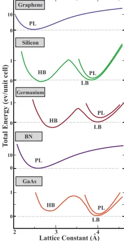
In Fig. 2 we show the variation in the total energy with respect to the lattice constant a of the 2D hexagonal Bravais lattice. We see that C and BN stayed planar and have a single minimum. The situation with Si, Ge, and GaAs is differ-ent since they have two other minima corresponding to LB and high-buckled 共HB兲 geometries in addition to planar geometry. In fact, the total energies corresponding to the minimum of the planar geometry are already higher than those of LB and HB geometries. In buckled geometries, while atoms of A sublattice are rising, those of B sublattice are lowered. At the end atoms of A and B sublattices lie in different planes having a buckling distance, ⌬ as shown in Fig.1. The value of⌬ in HB geometry is high and is in the ranges of ⬃2.5 Å but it is low in LB geometry and ranges between 0.4 and 0.7 Å. We note that two minima corre-sponding to HB and LB geometries in Fig.2are separated by TABLE I. Calculated results for group-IV elements, their binary compounds, and group III-V compounds having honeycomb structure. Stable structures are identified as PL or LB standing for the planar and low-buckled geometries, respectively. The values of angle between neighboring bonds,; buckling parameter, ⌬; nearest-neighbor distance, d; 2D hexagonal lattice constant, 兩aជ兩=兩a1 ជ兩=a; cohesive energy, Ec2 ;
minimum value of the energy gap, EGcalculated using LDA and corrected by GW0with the symmetry points indicating where minimum 共maximum兲 of conduction 共valence兲 band occurs; calculated effective charges on the constituent cation/anion, Zcⴱ/Zaⴱ; Poisson’s ratio,; and
in-plane stiffness, C, are given. Some of the structural parameters are described in Fig.1.
Geometry 共deg兲 共Å兲⌬ d 共Å兲 a 共Å兲 Ec 共eV兲 EG 共eV兲 Zcⴱ/Zaⴱ C 共J/m2兲 LDA-GW0 GROUP IV Graphene PL 120.0 1.42 2.46 20.08 Semimetal 0.0/0.0 0.16 335 Si LB 116.4 0.44 2.25 3.83 10.32 Semimetal 0.0/0.0 0.30 62 Ge LB 113.0 0.64 2.38 3.97 8.30 Semimetal 0.0/0.0 0.33 48 SiC PL 120.0 1.77 3.07 15.25 2.52/KM–4.19/KM 1.53/6.47 0.29 166 GeC PL 120.0 1.86 3.22 13.23 2.09/KK–3.83/KK 2.82/5.18 0.33 142 SnGe LB 112.3 0.73 2.57 4.27 8.30 0.23/KK–0.40/KK 3.80/4.20 0.38 35 SiGe LB 114.5 0.55 2.31 3.89 9.62 0.02/KK–0.00/KK 3.66/4.34 0.32 57 SnSi LB 113.3 0.67 2.52 4.21 8.72 0.23/KK–0.68/KK 3.89/4.11 0.37 40 SnC PL 120.0 2.05 3.55 11.63 1.18/⌫K–6.18/⌫K 2.85/5.15 0.41 98 III-V GROUP BN PL 120.0 1.45 2.51 17.65 4.61/KK–6.86/⌫K 0.85/7.15 0.21 267 AlN PL 120.0 1.79 3.09 14.30 3.08/⌫M–5.57/⌫M 0.73/7.27 0.46 116 GaN PL 120.0 1.85 3.20 12.74 2.27/⌫K–5.00/⌫K 1.70/6.30 0.48 110 InN PL 120.0 2.06 3.57 10.93 0.62/⌫K–5.76/⌫⌫ 1.80/6.20 0.59 67 InP LB 115.8 0.51 2.46 4.17 8.37 1.18/⌫K–2.88/⌫K 2.36/5.64 0.43 39 InAs LB 114.1 0.62 2.55 4.28 7.85 0.86/⌫⌫–2.07/⌫⌫ 2.47/5.53 0.43 33 InSb LB 113.2 0.73 2.74 4.57 7.11 0.68/⌫⌫–1.84/⌫⌫ 2.70/5.30 0.43 27 GaAs LB 114.7 0.55 2.36 3.97 8.48 1.29/⌫K–2.96/⌫K 2.47/5.53 0.35 48 BP PL 120.0 1.83 3.18 13.26 0.82/KK–1.81/KK 2.49/5.51 0.28 135 BAs PL 120.0 1.93 3.35 11.02 0.71/KK–1.24/KK 2.82/5.18 0.29 119 GaP LB 116.6 0.40 2.25 3.84 8.49 1.92/⌫K–3.80/KM 2.32/5.68 0.35 59 AlSb LB 114.8 0.60 2.57 4.33 8.04 1.49/KM–2.16/KK 1.58/6.42 0.37 35 BSb PL 120.0 2.12 3.68 10.27 0.39/KK–0.23/KK 3.39/4.61 0.34 91
a significant energy barrier. As we discuss in Sec. III Bthe minimum of HB is not actually a local minimum on Born-Oppenheimer surface. The sixfold rotation symmetry of graphene is broken as a result of buckling and changes to the threefold rotation symmetry C3. The similar symmetry breaking takes place also in group III-V compounds having PL honeycomb structures.
In concluding this discussion, we point out that even if the calculated total energy has a minimum relative to a specific structural parameter, this may not correspond to a local mini-mum. Then it remains to answer which of these minima in Fig. 2 corresponds to a local minima on the Born-Oppenheimer surface. At this point, reliable tests for stability of structure have to be performed.
A. Phonon modes and stability
Analysis of phonon modes provides a reliable test for a structure optimized conjugate gradient method. If there is an instability related with a phonon mode with k in BZ, the square of frequency,⍀共k兲 obtained from the dynamical ma-trix becomes negative yielding imaginary frequency. Then this particular mode cannot generate restoring force to ex-ecute lattice vibration and hence the system is vulnerable to go away from its original configuration. Phonon calculations are performed by taking into account the interactions in 共7⫻7⫻1兲 large supercells consisting of 98 atoms. For all the infinite 2D honeycomb structures, there are three acous-tical and three opacous-tical modes. In Fig. 3, we present the cal-culated dispersions of phonon modes of 22 honeycomb structures of group-IV elements and their binary compounds as well as group III-V compounds. These structures 共some being in PL and others in LB geometry兲 all have positive ⍀共k兲 in BZ indicating their stability. On the other hand, low-buckled Sn among group-IV elements and none of HB struc-tures are stable in the honeycomb form and hence they are not shown in Fig.3.
It is well known that as k→0 phonon dispersions of LA and TA branches are linear but that of ZA branch共due to out
of plane acoustical modes兲 is quadratic since transversal forces decay rapidly. Among these, the LA and TA phonon branches are heat-carrying modes. However, it was shown that bending branch ZA makes negligible contribution to thermal conductivity.57Note that the ZA branch becomes soft
and can easily get imaginary frequencies in BZ for certain honeycomb structures excluded in Fig. 3.
In our earlier paper43 we found that ZA mode of 2D
pe-riodic Ge honeycomb gets imaginary frequencies near ⌫ point of BZ. This situation has been interpreted as the bility against long-wavelength transversal waves. This insta-bility can be removed by the defects, such as ripples which do not allow these waves by limiting the size of Ge sheets. Finite size Ge honeycomb sheets can also be stabilized since long-wavelength transversal waves do not occur. Long wave-length defects in honeycomb structures have been treated earlier.11 An extensive analysis of phonon modes in the
present study revealed that the extent of the region of imagi-nary frequencies around the ⌫ point also depends on the mesh size used in the calculations. Decreasing the mesh size may lead to the decreasing of their particular zone. There-fore, a tedious analysis of the right mesh size is required to determine whether or not the imaginary frequency zone of ZA mode is an artifact of the mesh size. We performed this
Planar (PL) Low Buckled (Puckered)
∆ θ 120ο ο Top view Side view a2 a1
FIG. 1. Top and side views for two-dimensional共a兲 PL and 共b兲 LB 共or puckered兲 honeycomb structure. In the PL structure atoms are located on the same plane. In the LB structure the alternating atoms are located in two different parallel planes. The buckling⌬ is the distances between these two planes. Bravais lattice vectors for both structure are given with兩aជ兩=兩a1 ជ兩=a. The unitcell is delineated2
and shaded.
Lattice Constant (A)
Total Energy (ev /un it cell ) HB Germanium HB PL LB GaAs Silicon HB LB PL PL Graphene BN LB PL 0 10 0 1 0 10 0 1 0 1 o 2 3 4 PL
FIG. 2.共Color online兲 Variation in total energy of C, Si, Ge, BN, and GaAs honeycomb structures with respect to the lattice constant
a of 2D hexagonal lattice. The stable local minima of the
Born-Oppenheimer surface for each structure is shown with a dashed line separately.
analysis of mesh size for Ge-LB structure and found an op-timum fine mesh size where imaginary frequencies of ZA mode disappeared. We also note that since the interatomic forces related with ZA modes decay rapidly, the numerical inaccuracy in calculating forces due to the transversal dis-placement of distant atoms may give rise to difficulties in the treatment of ZA modes. Briefly, caution has to be exercised
in deciding whether the imaginary frequencies of ZA modes is an artifact of numerical calculations.
Calculated phonon dispersion of graphene is in good agreement with previous LDA results and also with reported experimental data.58–60 Around 1600 cm−1, LO and TO eigenmodes are degenerate at ⌫ point. In-plane TA and LA eigenmodes have linear dispersion around the ⌫ point. As it 0 4 8 12 16 0 1 2 3 4 5 6 0 2 4 6 8 10 12
Graphene Si-LB Ge-LB
SiC-PL 0 2 4 6 8 10 12 14 16 0 2 4 6 8 10 0 2 4 6 8
BN-PL AlN-PL GaN-PL InN-PL
0 1 2 0 1 2 3
GaAs-LB InP-LB InAs-LB InSb-LB
BP-PL BAs-PL AlSb-LB Ω (10 cm ) 2-1 Ω (10 cm ) 2-1 Ω (10 cm ) 2-1 Ω (10 cm ) 2-1 Γ Μ Κ Γ SnSi-LB 0 1 2 3 4 SiGe-LB 0 1 2 3 SnGe-LB 0 2 4 6 8 SnC-PL 0 2 4 6 8 10 GeC-PL Ω (10 cm ) 2-1 Ω (10 cm ) 2 -1 0 1 2 3 4 0 1 2 3 0 2 4 6 8 10 0 2 4 6 8 10 0 1 2 3 4 Γ Μ Κ Γ Γ Μ Κ Γ Γ0 Μ Κ Γ 2 4 6 8 BSb-LB
III-V GROUP BINARY COMPOUNDS
GROUP IV ELEMENTS & BINARY COMPOUNDS Γ Μ Κ Γ Γ Μ Κ Γ Γ Μ Κ Γ Γ Μ Κ Γ LA TA ZA ZO GaP-LB 0 1 2 3 4 5 0 2 4 6 8 0 1 2 3 4 5 0 1 2 3 LO TO
FIG. 3. 共Color online兲 Calculated vibration frequencies of phonon modes ⍀ versus k of group-IV elements, their binary compounds and group III-V compounds having honeycomb structure. Compounds having at least one constituent from first row elements have tendency to form planar structure. PL and LB stand for the planar and low-buckled共puckered兲 honeycomb structures, respectively.
is mentioned in earlier works on 2D structures, out-of-plane ZA eigenmode have quadratic phonon dispersion in the vi-cinity of⌫ point. Here, the calculated value for out-of-plane optical eigenmode ZO is around 900 cm−1. Existence of strong electron-phonon coupling in TO eigenmode at the K point and E2g modes at ⌫ point is the reason of the Kohn anomaly at these points. Therefore, scattering by phonon with the energies that corresponds to these modes can cause noticeable decrease in transmission spectrum.60,61 Since
force constant decreases with increasing atomic number or row number in the periodic table, calculated vibration fre-quencies exhibit the same trend.
As a result of symmetry in honeycomb structures of group-IV elements 共such as graphene, Si and Ge兲, ZO and TO branches cross at K point. We also note that the ZO branch of a binary compound comprising at least one ele-ment from the first row falls in the frequency range of acous-tical vibration modes. By comparing the phonon dispersions of InN, InP, InAs, and InSb samples, it is seen that ZO mode have increasing tendency to move apart from the LA and TA modes with increasing nearest-neighbor distance. However, in all the samples containing first row elements, ZO mode is located between the LA and TA modes. These characteristic trends of ZO mode exists for all the 2D honeycomb struc-tures.
B. Stability via puckering
According to analysis of stability based on the calculated phonon modes, structures which do not contain first row el-ements occur in LB共puckered兲 structure corresponding to a local minimum in Born-Oppenheimer surface. Through puckering the character of the bonding changes. Different hybrid orbitals underlie the different allotropic forms of C atom. While the bonding of diamond structure is achieved by tetrahedrally coordinated, directional sp3 hybrid orbitals, sp2+ pz and sp + px+ pyhybrid orbitals make the bonding in
graphene and cumulene 共monoatomic chain of carbon at-oms兲, respectively. In forming hybrid orbitals one of two valence s states is excited 共promoted兲 to p state whereby a promotion energy is implemented to the system. However, by s and p hybridization the hybrid orbitals yield the maxi-mum overlap between adjacent C-C atoms and hence the strongest possible bonding. This way, the promotion energy is compensated and the system attains cohesion. In sp3 hy-brid combination one s orbital is combined with px, py, and
pz orbitals to form four orbitals directed from the central C
atom toward its four nearest neighbors in tetrahedral direc-tions. The angle between these bonds is⬃109.5°. In sp2one s is hybridized with pxand pyorbitals to make three planar
sp2which are directed from the central C atom at the corners of the hexagons to its three nearest neighbors. For the cumu-lene s orbital is hybridized with pz orbital along the chain
axis. In this respect, the strengths共i.e., self-energy兲 of these hybrid orbitals decreases with increasing number of p-type orbitals in the combination; namely, sp is strongest whereas sp3 is least strong. As for the distance of C-C bonds, it is shortest in cumulene 共1.29兲 but longest in diamond 共1.53 Å兲. In addition to these hybrid orbitals, p orbitals
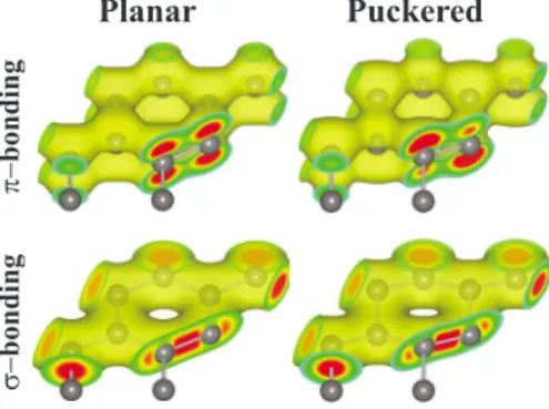
make also bonding between two C atoms. Thebonding between two adjacent C atoms in graphene and cumulene assures the planarity and linearity, respectively. In Fig.4the charge density of thebonds between neighboring C atoms explains how the stable planar geometry is maintained.
As the bond distance between two nearest-neighbor atoms increases, the overlap of the pz orbitals decreases. This, in
turn, decreases the strength of thebond. This is the situa-tion in the honeycomb structures of Si, where the Si-Si bond distance 共2.34 Å兲 increased by 92% relative to that of the C-C bond. As a result of weakerbonds the stability of the planar geometry cannot be maintained and the structure at-tains the stability through puckering, where three alternating atoms of a hexagon rise as the remaining three are lowered. At the end the structure is buckled by⌬. Through buckling the sp2hybrid orbital is dehybridized and s, p
x, and py
orbit-als are then combined with pz to form sp3-like orbitals.
While three sp3-like orbitals form covalent bonds with three nearest-neighbor atoms, one sp3-like orbital directed upward perpendicular to the atomic plane form a weak bond with the adjacent sp3-like orbital directed downward. The weak bond-ing between these adjacent sp3-like bonds is revealed from the isosurface charge density plots in Fig.4 as well as from the dispersion of the corresponding energy bands in Sec. V. The puckered Si honeycomb structure is reminiscent of graphane62–64with alternating C atoms saturated with
hydro-gen atoms from different sites. Briefly, puckering occurs as a result of weakening ofbonds whereby the structure regains its stability through tetrahedrally coordinated sp3-like bond-ing. Puckering may be explained in terms of Jahn-Teller theorem65 predicting that an unequal population of
degener-ate orbitals in a molecule leads to a geometric distortion. This way the degeneracy is removed and the total energy is lowered.
As shown in TableI, 11 out of 22 honeycomb structures prefer planar geometry, the rest is puckered to regain
stabil-Planar Puckered π− bond ing σ− bond ing
FIG. 4. 共Color online兲 Charge-density isosurfaces for and bonding: in the honeycomb structures of C, BN, and several others, the planar geometry is maintained by the strong bonding through the perpendicular pzorbitals, in addition to the bonding through the sp2hybrid orbitals. In the case of honeycomb structures formed
by the elements beyond the first row, the- bonding is weakened due to the increasing bond length and hence the structure is puck-ering where sp2 hybrid orbitals are slightly dehybridized to form sp3-like orbitals. This situation is depicted for Si honeycomb
struc-ture. Increasing charge density is plotted with colors from yellow 共light兲 to red 共dark兲.
ity. There are interesting examples for planar and puckered ring structures: besides BN, planar B共CH3兲3 molecule and well-known B共OH兲3 boric acid planar crystals are other ex-amples for boron-containing materials. Sn rings such as S7, S8, and S12 have also puckered structures with a crown shape.66 Another example is planar cyclobutadiene共C4H4兲;
the well-known molecule was shown that it lowers its energy when it has puckered共butterfly兲 structure for its positive di-anion 共C4H4+2兲. Additionally, it was shown before67 that
puckered shape of cyclooctatetraene C8H8takes planar shape for its negative dianion C8H8
−2
. For the phosphazenes 共NPX2兲, while N4P4F8 is planar N4P4Cl8 and N4P4共CH3兲8 have buckled shapes68,69and thus the rule regarding the
com-pounds including first row elements is still valid.
Having discussed the general aspects, we now concentrate on the optimized atomic structure and corresponding elec-tronic properties of stable honeycomb structures. Calculated values of atomic- and electronic-structural parameters are given in Table I. One notes that all 11 structures having planar geometry has at least one constituent from the first row elements of the periodic table; namely, C, B, and N. Since the radii of these atoms are relatively small, their pres-ence as one of the constituents assures that the bond length is small enough to keep strong bonding. This explains how the radius of constituent atoms enters as a crucial ingredient in the structure. The rest of the honeycomb structures in TableIincluding Si and Ge are puckered to have LB geom-etry.
Finally, we note that calculated results given in Table I display interesting trends depending on the radius of con-stituent elements or their row number in the periodic table. For example, the bond strength or cohesive energy Ec of a
honeycomb structure gets weaker as the atomic radii or the row number of the constituent elements increase. The corre-lation between the cohesive energy, Ec, and lattice constant,
a and also that between the in-plane stiffness, C, and cohe-sive energy, Ec, are shown in Fig.5.
IV. MECHANICAL PROPERTIES
Honeycomb structure with sp2 bonding underlies the un-usual mechanical properties providing very high in-plane strength but transversal flexibility. We note that graphene and its rolled up forms, carbon nanotubes are among the stron-gest and stiffest materials yet discovered in terms of tensile strength and elastic modulus. We investigated the mechanical properties of 22 stable honeycomb structures listed in Table I. We focused on the harmonic range of the elastic deforma-tion, where the structure responded to strain ⑀ linearly. We pulled the rectangular unit cell in x and y directions in vari-ous amounts and generated a mesh of data corresponding to the strains in x and y directions versus strain energy defined as Es= ET共⑀兲−ET共⑀= 0兲; namely, the total energy at a given
strain ⑀ minus the total energy at zero strain. The data is fitted to a two-dimensional quadratic polynomial expressed by ES共⑀x,⑀y兲 = a1⑀x 2 + a2⑀y 2 + a3⑀x⑀y, 共2兲
where⑀xand⑀yare the small strains along x and y directions
in the harmonic region. Owing to the isotropy of the honey-comb structure a1= a2. The same equation can be obtained from elastic tensor70 in terms of elastic stiffness constants,
namely, a1= a2=共h·A0/2兲·C11; a3=共h·A0兲·C12. Hence one obtains Poisson’s ratio = −⑀trans/⑀axial, which is equal to
C12/C11= a3/2a1. Similarly, the in-plane stiffness, C = h · C11·关1−共C11/C12兲2兴=关2a1−共a3兲2/2a1兴/共A0兲. Here h and A0 are the effective thickness and equilibrium area of the system, respectively. In Table I, calculated Poisson’s ratio and in-plane stiffness results are shown. The calculated value of the in-plane stiffness of graphene is in agreement with the experimental value of 340⫾50 共N/m兲.71 Graphene has
highest in-plane stiffness and lowest Poisson’s ratio among all honeycomb structures of group-IV elements and group III-V compounds. Being a compound of first row elements, BN has second highest C and second lowest. The Poisson’s ratio increases with increasing row number of elements of
10 15 20 0 50 100 150 200 250 300 350 In-plane Stiffness (J/m 2) Graphene BN SiC AlN BP GeC GaN SnC BAs InN BSb Si SiGe Insb GaP
Cohesive Energy (eV)
2.5 3.0 3.5 4.0 4.5 8 10 12 14 16 18 20 Cohesive Energy (eV)
Lattice Constant (A)
Graphene BN SiC AlN Insb BAs SnC Si BSb GaP Alsb InAs SnSi BP GeC GaN InN SiGe o
FIG. 5. 共Color online兲 A plot showing the correlation between the cohesive energy Ecand lattice constant共left兲 and between in-plane stiffness C and Ecamong honeycomb structures studied in this work. Squares and circles are for PL and LB structures, respectively.
elemental and compound honeycomb structures. C shows a reverse trend. The order of values of C in the last column of TableIis similar to that of cohesive energies Ecin the
sev-enth column. This clearly indicates a correlation between Ec
and C as shown in Fig.5.
V. ELECTRONIC STRUCTURE
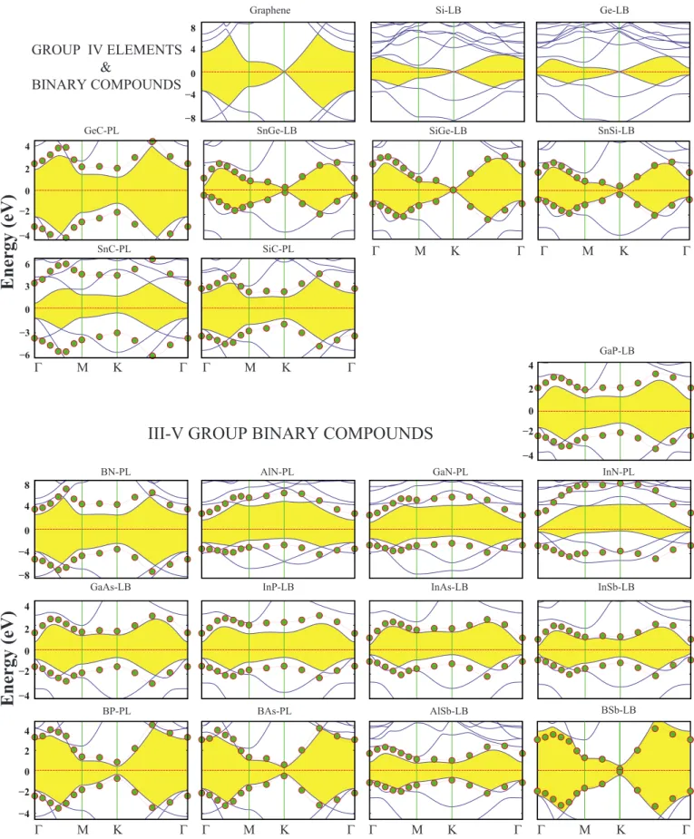
Our results on the electronic-band structure of group-IV elements and binary compounds between different group-IV elements and group III-V elements, which are stable in either infinite periodic form or in finite size, are presented in Fig.6. In these hexagonal lattice structures 共PL or LB兲 relevant electronic-energy bands around the Fermi level are derived from and ⴱ bands. In elemental honeycomb structures, such as graphene, Si and Ge, these bands have linear cross-ings at two inequivalent K and K
⬘
points of BZ, called Dirac points and hence they are semimetallic. Because of their lin-ear dispersion of E共k兲, the charge carriers near the Dirac points behave as massless Dirac fermions. By fitting the andⴱ bands at k = K + q to the expressionE共q兲 ⯝ vFប兩q兩 + O共q2兲 共3兲 and neglecting the second-order terms with respect to q2, one can estimate the Fermi velocity for both Si and Ge as vF
⬃106 m/s. We note that v
F calculated for 2D LB
honey-comb structures of Si and Ge are rather high and close to that calculated for graphene using the tight-binding bands. It is also worth noting that because of the electron-hole symmetry at K and K
⬘
points of BZ, 2D LB Si and Ge are ambipolar for E共q兲=EF⫾␦E,␦E being small.In graphene Dirac fermions have a high Fermi velocity, vF= c/300. Due to its high carrier mobility, graphene-based
ballistic transistors operating at room temperature have al-ready been fabricated.72 In addition to these unusual
elec-tronic properties of graphene, the observation of anomalous quantum Hall effect and the possibility of Klein paradox are features, which attract the interest of researchers. Electronic properties of graphene and graphene-based structures have recently been reviewed.73,74
In the polar structures, such as BN, GaAs, after charge-transfer pzorbital electrons are located predominantly on one
type of atom. Thus the degeneracy of valence and conduction bands at K point is removed and gap opening occurs.75 In
Table I the minimum width of band gaps calculated with LDA are given together with the symmetry points where the maximum 共minimum兲 of valence 共conduction兲 bands occur. Values of these band gaps after a correction by the GW0 method are also given. The bands of compounds before and after GW0correction are also illustrated in Fig.6.
Binary compounds have polar character in addition to the covalency of bonds. Effective charge on cation and anion, Zcⴱ
and Zaⴱ, charge transferred from cation to anion, ␦= Zaⴱ− Zv
共Zvbeing the valency of the constituent atom兲 are calculated
using Bader analysis. In spite of the ambiguities in finding the true effective charge, the calculated effective charges in TableIgive some idea about the direction of charge transfer and ionicity of the honeycomb structure. For some binary compounds such as SiC, BN, and AlN calculated effective
charges appear to be right in sign but exaggerated in magni-tude. We note that as the difference in the row numbers of constituent elements increases, Zⴱusually decreases. One can also generalize that the charge transfer decreases with in-creasing row number or atomic radii of anion if the cation is fixed. This trend is obvious in the structures of InN, InP, InAs, and InSb.
VI. HETEROSTRUCTURES
Depending on the constituent elements the band gaps of compound honeycomb structures change in a wide energy range. In contrast, the lattice constant a of the compounds do not show significant variation. The situation, where band gaps of two honeycomb structures are significantly different while their lattice constants are practically the same, is a convenient condition to make semiconductor heterostru-cures. As an example, let us consider AlN and GaN, which have LDA band gaps of 3.08 and 2.27 eV, respectively. Their lattice constants are not significantly different and are 3.09 and 3.20 Å, respectively. Moreover, armchair nanoribbons can form pseudomorphic heterostructure with perfect junc-tion. This is reminiscent of an AlN/GaN commensurate het-erostructure having 2D interface. Owing to charge transfer between constituent nanoribbons at the junction, the bands are shifted and eventually aligned. Heterostructures of el-emental and compound semiconductors generating a 2D electron gas and devices produced therefrom have been an active field of study in device physics in the past decades. It is expected that the heterostructure of armchair nanoribbons of GaN and AlN can constitute a 1D analog. When periodi-cally repeated, this heterostructure can form superlattices be-having as multiple quantum wells or quantum dots. Earlier similar effects have been investigated for the heterostructures of graphene nanoribbons with different widths.24
Superlattices of armchair honeycomb nanoribbon struc-tures can be constructed according to the width and repeat periodicity of the constituent segments. We can label GaN/ AlN superlattices as GaN/AlN共n1, n2; s1, s2兲. Here, s1and s2 specify the length of segments in terms of the numbers of the unit cells of constituent nanoribbons. Also n1and n2specify the width in terms of the number of dimer lines in the primi-tive unit cell of constituent nanoribbons. By varying the n and s, we can construct variety of superlattice structures. As a proof of concept, we consider a superlattice Ga-NAlN共10,10;4,4兲 as shown in Fig.7. In the same figure we also presented the electronic-band structure of constituent GaN and AlN nanoribbons. Upon construction, the atomic structure is fully optimized. Resulting energy band-structure and charge-density isosurfaces are presented in the same fig-ure.
The highest valence-band and the lowest conduction-band states are flat and they are identified as confined states. As a result, one can deduce a type-I 共normal兲 band alignment since states are confined to the GaN part of heterostructure. One notes that the bandgap of the superlattice in momentum space is different from those of constituent nanoribbons and can also expect that the superlattice band gap in momentum space gets larger as the extension of GaN and AlN sides
−6 −3 0 3 6 −8 −4 0 4 8 −4 −2 0 2 4 −8 −4 0 4 8 −4 −2 0 2 4 −4 −2 0 2 4
Energy
(eV)
Energy
(eV)
Graphene Si-LB Ge-LB
GeC-PL SnGe-LB SiGe-LB SnSi-LB
SnC-PL SiC-PL
GaP-LB
BSb-LB
GaAs-LB InP-LB InAs-LB InSb-LB
BP-PL BAs-PL AlSb-LB −4 −2 0 2 4 GROUP IV ELEMENTS & BINARY COMPOUNDS
III-V GROUP BINARY COMPOUNDS
BN-PL AlN-PL GaN-PL InN-PL
Γ Μ Κ Γ Γ Μ Κ Γ Γ Μ Κ Γ Γ Μ Κ Γ
Γ Μ Κ Γ Γ Μ Κ Γ
Γ Μ Κ Γ Γ Μ Κ Γ
FIG. 6.共Color online兲 Energy bands of monolayer honeycomb structures of Group-IV elements and binary compounds between different group-IV elements and group III-V elements. All the group-IV elements have semimetallic electronic structure. Band structures show that like graphene and ⴱbands of Si and Ge have linear band crossing at the Fermi level. Binary compounds of group-IV and group III-V elements are semiconductors. Corrections LDA band gaps using GW0are indicated by small circles. Band gaps are shaded.
increases. Similar confined states can be obtained by con-structing AlN core and GaN shell structures, where electrons are expected to be confined in the core region.
VII. DISCUSSIONS AND CONCLUSIONS
In view of the exceptional electronic, magnetic, and me-chanical properties of recently synthesized graphene, ques-tions have been raised whether well-known materials in mi-croelectronic and optoelectronic industry can attain similar honeycomb structures. It is hoped that unusual properties can
be attained from these structures. The present paper exam-ined a large number of materials, group-IV elements, binary compounds of these elements, as well as a large number of group III-V compounds to reveal whether they may form 2D honeycomb structure. For several decades, the bulk crystals of these materials have dominated microelectronic and opto-electronic industry. Based on ab initio structure optimization and calculations of phonon modes we are able to determine 22 honeycomb structures, which can be stable in a local minimum on the Born-Oppenheimer surface as either 2D infinite periodic crystals or finite-size flakes 共patches兲. Our calculations reveal that group-IV elements, Si and Ge, and binary compounds SiC, GeC, SnC, SnSi, SnGe, and SiGe have stable honeycomb structures. However, while SiC, GeC, and SnC are planar like graphene and BN, Si, Ge, SnSi, SnGe, and SiGe are buckled共or puckered兲 for stabili-zation. We also find that all III-V compounds containing first row elements B, C, or N have planar stable structures. How-ever, the binary compounds formed from the combination of Al, Ga, In and P, As, Sb are found to be stable in low-buckled structure. It should be noted that the present study does not exlcude the occurrence of other local minima which may be more energetic than these 2D honeycomb structures. For honeycomb structures which were deduced to be stable, an extensive analysis has been carried out to deter-mine their atomic structure, elastic and electronic properties. While Si and Ge are semimetallic and have linear band crossing at the Fermi level like graphene, all the binary com-pounds are found to be semiconductors. It is also seen that honeycomb structures of group-IV elements and III-V binary compounds exhibit interesting correlations among the cohe-sive energy, lattice constant, band gap, effective charge, in-plane stiffness, and Poisson’s ratio.
These materials in honeycomb structure have a variety of band gaps. Even more remarkable is that the nanoribbon13
forms of these materials provide diverse properties depend-ing on not only their constituents but also their chirality76,77
and width. All these properties are expected to offer number of applications. Therefore, the studies related with their functionalization78by vacancy defects or adatoms, their
me-chanical and spintronic properties, their heterostructures and core-shell structures will open a field of research. We hope that the findings in this work will promote the research aim-ing at the synthesis of these materials.
ACKNOWLEDGMENTS
Computing resources used in this work were provided by the National Center for High Performance Computing of Turkey 共UYBHM兲 under Grant No. 2-024-2007. This work was partially supported by TÜBITAK under Grant No. 106T597. S.C and R.T.S acknowledge financial support from TÜBA共Turkish Academy of Sciences兲.
Γ Ζ
Energy
(eV)
3 1 2 0 -2 -1 -3 quantum wellGaN
AlN
Γ Ζ Ζ ΓGaN AlN GaN /AlN
(a)
GaN n1=10 n2=10 AlNGaN/AlN Superlattice
(b)
(c)
y x BANDS CHARGES EF s2=4 s1=4 Unit cellFIG. 7. 共Color online兲 共a兲 A superlattice formed by periodically repeating heterostructure of armchair nanoribbons of GaN-AlN compounds. Red, yellow, blue, and small balls represent Ga, Al, N, and H atoms, respectively.共b兲 Energy band structures of constituent GaN, AlN nanoribbons, and resulting superlattice in momentum space. The band gaps are shaded by yellow.共c兲 Band decomposed isosurface charge densities for lowest two conduction band and highest two valence bands. Charges of lowest conduction-band and highest valence-band states are confined in GaN side of the junc-tion, which has relatively smaller band gap than AlN.
1K. S. Novoselov, A. K. Geim, S. V. Morozov, D. Jiang, Y.
Zhang, S. V. Dubonos, I. V. Grigorieva, and A. A. Firsov, Sci-ence 306, 666共2004兲.
2P. R. Wallace, Phys. Rev. 71, 622共1947兲.
3M. I. Katsnelson, K. S. Novoselov, and A. K. Geim, Nat. Phys. 2, 620共2006兲.
4K. S. Novoselov, A. K. Geim, S. V. Morozov, D. Jiang, M. I.
Katsnelson, I. V. Grigorieva, S. V. Dubonos, and A. A. Firsov, Nature共London兲 438, 197 共2005兲.
5C. Itzykson and J.-B. Zuber, Quantum Field Theory 共Dover,
New York, 2006兲.
6A. Calogeracos and N. Dombey, Contemp. Phys. 40, 313
共1999兲.
7C. Berger, Z. Song, T. Li, X. Li, A. Y. Ogbazghi, R. Feng, Z.
Dai, A. N. Marchenkov, E. H. Conrad, P. N. First, and W. A. de Heer, Science 312, 1191共2006兲.
8Y. Zhang, Yan-Wen Tan, H. L. Stormer, and P. Kim, Nature
共London兲 438, 201 共2005兲.
9N. D. Mermin, Phys. Rev. 176, 250共1968兲.
10P. Le Doussal and L. Radzihovsky, Phys. Rev. Lett. 69, 1209
共1992兲.
11A. Fasolino, J. H. Los, and M. I. Katsnelson, Nature Mater. 6,
858共2007兲.
12J. C. Meyer, A. K. Geim, and M. I. Katsnelson, Nature共London兲 446, 60共2007兲.
13Y. W. Son, M. L. Cohen, and S. G. Louie, Phys. Rev. Lett. 97,
216803共2006兲.
14V. Barone, O. Hod, and G. E. Scuseria, Nano Lett. 6, 2748
共2006兲.
15K. I. Sasaki, S. Murakami, and R. Saito, J. Phys. Soc. Jpn. 75,
074713共2006兲.
16D. A. Abanin, P. A. Lee, and L. S. Levitov, Phys. Rev. Lett. 96,
176803共2006兲.
17D. A. Areshkin, D. Gunlycke, and C. T. White, Nano Lett. 7, 204
共2007兲.
18M. Ezawa, Phys. Rev. B 73, 045432共2006兲. 19K. Kobayashi, Phys. Rev. B 48, 1757共1993兲.
20M. Fujita, K. Wakabayashi, K. Nakada, and K. Kusakabe, J.
Phys. Soc. Jpn. 65, 1920共1996兲.
21K. Nakada, M. Fujita, G. Dresselhaus, and M. S. Dresselhaus,
Phys. Rev. B 54, 17954共1996兲.
22K. Wakabayashi, M. Sigrist, and M. Fujita, J. Phys. Soc. Jpn. 67,
2089共1998兲.
23Y.-W. Son, M. L. Cohen, and S. G. Louie, Nature共London兲 444,
347共2006兲.
24M. Topsakal, H. Sevinçli, and S. Ciraci, Appl. Phys. Lett. 92,
173118共2008兲; H. Sevincli, M. Topsakal, and S. Ciraci, Phys. Rev. B 78, 245402共2008兲.
25H. Şahin and R. T. Senger, Phys. Rev. B 78, 205423共2008兲. 26J. Y. Yan, P. Zhang, B. Sun, H.-Z. Lu, Z. Wang, S. Duan, and
X.-G. Zhao, Phys. Rev. B 79, 115403共2009兲.
27K. S. Novoselov, D. Jiang, F. Schedin, T. Booth, V. V.
Khot-kevich, S. Morozov, and A. K. Geim, Proc. Natl. Acad. Sci. U.S.A. 102, 10451共2005兲.
28D. Pacilé, J. C. Meyer, Ç. Ö. Girit, and A. Zettl, Appl. Phys.
Lett. 92, 133107共2008兲.
29Z. Zhang and W. Guo, Phys. Rev. B 77, 075403共2008兲. 30C. H. Park and S. G. Louie, Nano Lett. 8, 2200共2008兲. 31V. Barone and J. E. Peralta, Nano Lett. 8, 2210共2008兲.
32M. Topsakal, E. Akturk, and S. Ciraci, Phys. Rev. B 79, 115442
共2009兲.
33Y. Wang, X. Fan, and J. Sun, Mater. Lett. 63, 350共2009兲. 34Y. Huang, J. He, Y. Zhang, Y. Dai, Y. Gu, S. Wang, and C. Zou,
J. Mater. Sci. 41, 3057共2006兲.
35J. Duan, Xintang Huang, E. Wang, Mater. Lett. 60, 1918共2006兲. 36G. S. Wu, T. Xie, X. Y. Yuan, Y. Li, L. Yang, Y. H. Xiao, and L.
D. Zhang, Solid State Commun. 134, 485共2005兲.
37M. Topsakal, S. Cahangirov, and E. Bekaroglu, arXiv:0907.3070
共unpublished兲.
38C. Tusche, H. L. Meyerheim, and J. Kirschner, Phys. Rev. Lett. 99, 026102共2007兲.
39A. R. Botello-Mendez, F. Lopez-Urias, M. Terrones, and H.
Ter-rones, Nano Lett. 8, 1562共2008兲.
40A. R. Botello-Mendez, M. T. Martinez-Martinez, F. Lopez-Urias,
M. Terrones, and H. Terrones, Chem. Phys. Lett. 448, 258 共2007兲.
41L. Sun, Y. Li, Z. Li, Q. Li, Z. Zhou, Z. Chen, J. Yang, and J. G.
Hou, J. Chem. Phys. 129, 174114共2008兲.
42E. Bekaroglu, M. Topsakal, S. Changirov, and S. Ciraci
共unpub-lished兲.
43S. Cahangirov, M. Topsakal, E. Akturk, H. Şahin, and S. Ciraci,
Phys. Rev. Lett. 102, 236804共2009兲.
44K. Takeda and K. Shiraishi, Phys. Rev. B 50, 14916共1994兲. 45E. Durgun, S. Tongay, and S. Ciraci, Phys. Rev. B 72, 075420
共2005兲.
46H. Nakano, T. Mitsuoka, M. Harada, K. Horibuchi, H. Nozaki,
N. Takahashi, T. Nonaka, Y. Seno, and H. Nakamura, Angew. Chem. 118, 6451共2006兲.
47R. Krishnan, Q. Xie, J. Kulik, X. D. Wang, S. Lu, M. Molinari,
Y. Gao, T. D. Krauss, and P. M. Fauchet, J. Appl. Phys. 96, 654 共2004兲.
48G. Kresse and J. Hafner, Phys. Rev. B 47, 558共1993兲. 49G. Kresse and J. Furthmüller, Phys. Rev. B 54, 11169共1996兲. 50P. E. Blochl, Phys. Rev. B 50, 17953共1994兲.
51R. M. Martin, Electronic Structure共Camridge University Press,
Camridge, 2004兲.
52D. M. Ceperley and B. J. Alder, Phys. Rev. Lett. 45, 566共1980兲. 53H. J. Monkhorst and J. D. Pack, Phys. Rev. B 13, 5188共1976兲. 54M. Shishkin and G. Kresse, Phys. Rev. B 74, 035101共2006兲. 55G. Henkelman, A. Arnaldsson, and H. Jonsson, Comput. Mater.
Sci. 36, 354共2006兲.
56D. Alfè, Comput. Phys. Commun. 180, 2622共2009兲. 57P. G. Klemens, Int. J. Thermophys. 22, 265共2001兲. 58I. H. Lee and R. M. Martin, Phys. Rev. B 56, 7197共1997兲. 59S. Narasimhan and S. de Gironcoli, Phys. Rev. B 65, 064302
共2002兲.
60J.-A. Yan, W. Y. Ruan, and M. Y. Chou, Phys. Rev. B 77, 125401
共2008兲.
61S. Piscanec, M. Lazzeri, F. Mauri, A. C. Ferrari, and J.
Robert-son, Phys. Rev. Lett. 93, 185503共2004兲.
62J. O. Sofo, A. S. Chaudhari, and G. D. Barber, Phys. Rev. B 75,
153401共2007兲.
63D. C. Elias, R. R. Nair, T. M. G. Mohiuddin, S. V. Morozov, P.
Blake, M. P. Halsall, A. C. Ferrari, D. W. Boukhvalov, M. I. Katsnelson, A. K. Geim, and K. S. Novoselov, Science 323, 610 共2009兲.
64H. Şahin, C. Ataca, and S. Ciraci, arXiv:0907.0549
共unpub-lished兲.
共1937兲.
66B. Meyer, Adv. Inorg. Chem. Radiochem. 18, 297共1976兲. 67B. Webster, Chemical Bonding Theory 共Blackwell, Oxford,
1990兲.
68J. F. Labarre, Struct. Bonding共Berlin兲 35, 1 共1978兲.
69R. Hazekamp, T. Migchelsen, and A. Vos, Acta Crystallogr. 15,
539共1962兲.
70J. F. Nye, Physical Properties of Crystals 共Clarendon, Oxford,
1985兲.
71C. Lee, X. Wei, J. W. Kysar, and J. Hone, Science 321, 385
共2008兲.
72X. Wang, Y. Ouyang, X. Li, H. Wang, J. Guo, and H. Dai, Phys.
Rev. Lett. 100, 206803共2008兲.
73A. K. Geim and K. S. Novoselov, Nature Mater. 6, 183共2007兲. 74A. H. Castro Neto, F. Guinea, N. M. R. Peres, K. S. Novoselov,
and A. K. Geim, Rev. Mod. Phys. 81, 109共2009兲.
75W. A. Harrison, Electronic Structure and Properties of Solids-The Physics of Chemical Bonds共Freeman, San Francisco, 1980兲. 76A. Lherbier, B. Biel, Y. M. Niquet, and S. Roche, Phys. Rev.
Lett. 100, 036803共2008兲.
77F. Cervantes-Sodi, G. Csanyi, S. Piscanec, and A. C. Ferrari,
Phys. Rev. B 77, 165427共2008兲.
78E. Durgun, S. Dag, O. Gulseren, and S. Ciraci, J. Phys. Chem. B 108, 575共2004兲; H. Sevincli, M. Topsakal, E. Durgun, and S.