First-principles study of GaAs nanowires
S. Cahangirov1and S. Ciraci1,2,*
1UNAM, Institute for Materials Science and Nanotechnology, Bilkent University, Ankara 06800, Turkey 2Department of Physics, Bilkent University, Ankara 06800, Turkey
共Received 24 December 2008; revised manuscript received 17 March 2009; published 28 April 2009兲
In this paper we present a detailed analysis of the atomic and electronic structures of GaAs nanowires using first-principles pseudopotential calculations. We consider six different types of nanowires with different diam-eters all grown along关111兴 direction, and we reveal interesting trends between cohesive energy and nanowire type with varying diameters. Generally, the average cohesive energy of nanowires with wurtzite stacking is higher than those with zinc-blende stacking for small diameters. We found that most of the bare nanowires considered here are semiconducting and continue to be semiconducting upon the passivation of surface dan-gling bonds with hydrogen atoms. However, the surface states associated with the surface atoms having two dangling bonds in zinc-blende stacking occur in the band gap and can decrease the band gap to change the nanowire from semiconducting to metallic state. These nanowires become semiconducting upon hydrogen passivation. Even if the band gap of some nanowires decreases with increasing diameter and hence reveals the quantum confinement effect, generally the band-gap variation is rather complex, and depends on the type and geometry, diameter, type of relaxation, and also whether the dangling bonds of surface atoms are saturated with hydrogen.
DOI:10.1103/PhysRevB.79.165118 PACS number共s兲: 61.46.Km, 62.23.Hj, 73.22.⫺f
I. INTRODUCTION
In searching to discover semiconductor materials and me-tallic interconnect for new generation miniaturized electronic devices, nanostructures have been a focus of attention. Electronic devices, such as transistors based on carbon nanotubes,1attracted interest in nanowires. Rodlike Si nano-wires have been fabricated2 with a diameter of 1.3–7 nm.3 It has been shown that such Si nanowires can display metal-lic, semiconducting, and half-metallic properties depending on their functionalization.4 Being an alternative to silicon based microelectronics GaAs is one of the most important materials used in semiconductor physics. Due to the high electron mobility, GaAs always carried a potential of being used in high-speed electronic devices. GaAs/AlGaAs heterostructures5 have served as media for the two-dimensional electron-gas studies.
Similar to bulk crystals researcher have envisioned GaAs nanowires to be a potential alternative for Si nanowires. Re-cent advances in fabrication technology made it possible to grow GaAs nanowires. They are grown by metal catalysts in vapor-liquid-solid 共VLS兲 mechanism.6 Generally, GaAs nanowires are grown along 关111兴 direction in zinc-blende 共zb兲 structure, whereas nanowires with wurtzite 共wz兲 struc-ture with diameter as small as 10 nm are also observed.7 Several models were developed to predict the transition ra-dius from wurtzite to zinc-blende structure.8,9Actually, there is no sharp transition but instead there are many different stacking configurations with very similar energies and more sophisticated models are needed to predict the ground-state configuration. Together with the crystal structure, surface facet structure is also an important parameter affecting the structural and electronic properties. Nanowires reported so far are either grown in zb structure with关112¯兴 or 关11¯0兴 facet orientation, or in wz structure with 关11¯00兴 or 关112¯0兴 facet orientation.10–12One of the unusual structures is so-called A
wire, which has been grown in defect free triangular shape on 共111兲A surface of GaAs.13 More complex structure of nanowires grown on GaAs共111兲B surface has been also reported.14
There are many experimental and theoretical works on growth and structure of GaAs nanowires but not much work is done to predict the electronic properties of these wires. Theoretical studies so far have focused on the electronic properties of superlattices composed of GaAs nanowires. For example, the electronic structure of InAs/GaAs nanowire su-perlattices with radius R = 10 nm was examined using a semiempirical sp3d5sⴱ tight-binding model.15Another atom-istic tight-binding calculation was carried out to reveal the electronic structure of freestanding GaAs/Al0.3Ga0.7As nano-wire superlattices oriented along the 关100兴 crystallographic direction.16Also a first-principles investigation has been per-formed on the hexagon-shaped 关111兴/关0001兴-oriented III–V semiconductor nanowires, which was concentrated on the surface effects on the structure and stability of these nanowires.10
The purpose of this paper is to provide a detailed analysis of GaAs nanowires, which is necessary for further experi-mental and theoretical studies. To this end we present a sys-tematic first-principles investigation on structural and elec-tronic properties of GaAs nanowires grown along 关111兴 direction. Six different types of GaAs nanowires are distin-guished depending on the shape of their cross sections and the crystallographic orientation of their side surfaces. Their optimized atomic structure and cohesive energies are calcu-lated revealing interesting trends between atomic structure and cohesive energy. Based on the calculations of electronic structure and isosurface charge density of specific states, we analyzed the character of states at the band edges and varia-tion in band gap with diameter. The effects of hydrogen satu-ration of dangling bonds of surface atoms on the atomic and electronic structure are examined. We found that most of bare GaAs nanowires are semiconducting and remain
semi-conducting even before the passivation of surface dangling bonds. Only one type is metallic due to the states localized at the surface.
II. METHODS
We have performed first-principles plane-wave calculations17,18within density-functional theory共DFT兲 共Ref.
19兲 using ultrasoft pseudopotentials.18,20 The pseudopoten-tials having three electrons for Ga共4s24p1兲, five electrons for As 共4s24p3兲, and one electron for H 共1s1兲 were used. A plane-wave basis set with kinetic energy up to 250 eV was used. Cutoff energies used were at least 30% higher than maximum values suggested.18The exchange-correlation po-tential is approximated by generalized gradient approxima-tion 共GGA兲 using PW91 functional.21 For partial occupan-cies we use the Methfessel-Paxton smearing method.22 The adopted smearing width is 0.1 eV for the atomic relaxation, and 0.01 for the accurate band-structure analysis and density of state calculations. All structures have been treated within a supercell geometry using the periodic boundary conditions. Vacuum spacing was arranged so that the minimum distance between two atoms in adjacent unit cells were larger than 10 Å, provided that atoms have negligible interaction at that far distances. We chose bare wz3 – 96 as a test structure and increased the vacuum spacings to 16 Å. This resulted in an energy difference around 0.2 meV/atom. In the self-consistent potential and total-energy calculations the Bril-louin zone共BZ兲 is sampled in the k space within Monkhorst-Pack scheme23 by 共1⫻1⫻9兲 mesh points for wz and 共1 ⫻1⫻7兲 mesh points zb nanowires. Increasing the k-space sampling for bare wz3 – 96 structure from 共1⫻1⫻9兲 to 共1 ⫻1⫻15兲 resulted in a total-energy difference around 1 meV. All atomic positions and lattice constant are optimized by using the conjugate gradient method where total energy and atomic forces are minimized. The criterion of convergence for energy is chosen as 10−5 eV between two ionic steps, and the maximum force allowed on each atom is 0.05 eV/Å. We have reduced the maximum force criterion down to 0.0025 eV/Å in our test structure, bare wz3–96. This had no considerable effect since the change in energy and band gap was around 0.3 meV/atom and 0.006 eV, respectively. Clearly, the criterion for the maximum allowed force 0.05 eV/Å is appropriate for systems including large num-ber of atoms.
III. STRUCTURES AND COHESIVE ENERGIES
GaAs nanowires studied here are cut from ideal bulk structure along 关111兴 direction. Nanowires having wurtzite 共wz兲 and zinc-blende 共zb兲 stackings have four and six atomic layers in the unit cell, respectively. Except A wire, they have hexagonal cross section. A wires by themselves have zb stacking and display a triangular cross section with three 共112¯兲 planar side surfaces. Atomic structures of cross section of all nanowires are shown before and after relaxation 共struc-ture optimization兲 in Fig. 1. Here we consider the largest members of all types of GaAs nanowires. Upon relaxation the surfaces of ideal wires undergo a reconstruction while
inner parts preserve the bulk configuration. In spite of the fact that the indices of their planar side surface are the same, wz1 and wz3 are still different. wz3 structure have six iden-tical surfaces, whereas wz1 structure have three surfaces same as wz3 and three surfaces with hanging Ga-As atom pairs before relaxation.
At the surfaces of some ideal structures in Fig. 1 the at-oms can have the coordination number smaller than four. Upon relaxation the coordination numbers may undergo a change. Two adjacent surface atoms having low coordination number can form new bonds, whereby these atoms increase their coordination number and the nanowire, in turn, lowers its energy共i.e., it becomes more energetic兲. It turns out that the coordination number of surface atoms is crucial for the value of the cohesive energy per atom pair. For example, wz1 nanowire with N = 109 has three surfaces each having an atom pair with coordination number of two while other three surfaces have surface atoms with coordination number of three. wz2 nanowires having N = 25, 60, and 85 atom pairs in the unit cell have surface atoms with coordination number of two only at the corners of the hexagonal cross section. On the other hand, wz2 nanowires having N = 42 and 114 atom pairs in the unit cell, and all members of wz3 nanowires have surface atoms with coordination number of three. In light of these arguments one expects wz3 to have larger cohesive
FIG. 1. 共Color online兲 Ideal and relaxed atomic structures of bare GaAs nanowires considered in this paper. Numerals given in parenthesis indicate the crystallographic directions perpendicular to the surfaces. Numerals given to the bottom left of the structures stand for the number of atom pairs per unit cell N. wz and zb stand for structures having wurtzite and zinc-blende stackings.
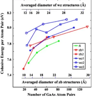
energy per atom pair than the rest of wz2 nanowires, which, in turn, should be larger than that of wz1 nanowires. These arguments are actually confirmed in Fig.2, where we present the trends of cohesive energies per atom pair for all nano-wires considered here.
Ideal A wires have surface atoms with coordination num-ber of two on each surface, but apart from that, it has a triangular cross section, which makes the surface-to-volume ratio even higher compared to that of other types. Conse-quently, A wires have the lowest cohesive energy per atom pair as seen in Fig.2.
Interestingly, wz structures have relatively larger cohesive energies than zb structures, with wz3 structure being the larg-est. The bulk zb structure however is energetically more fa-vorable than that of wz structure by nearly 20 meV per Ga-As pair, also confirmed by our calculations. As radii
in-crease, the cohesive energy per Ga-As atom-pair values should converge to the bulk value. It is energetically easier to form a wz surface than to form a zb surface. In other words surface energy of zb structure is larger. That is why, wz struc-tures become energetically more favorable as the surface-to-volume ration increases, namely, as the radius of the nano-wire decreases. So there should be some point where cohesive energy of wz and zb structures cross each other. The radius at this point can be interpreted as the critical radius for transition from wz to zb structure or vice versa. Here it should be noted that energetically favorable does not mean that these structures will start to grow in experiments. One should also include effects of formation path, such as nucle-ation growth. Actually, when we are around the critical ra-dius we can see some hybrid stacking patterns such as ABAC, which is defined as 4H structure.9
Table I gives the calculated values for the structure and cohesive energies of nanowires after the relaxation. Cohesive energies per Ga-As atom pair increase with increasing diam-eter, approaching the bulk values, but we do not see the critical radius because it is expected to be an order-of-magnitude larger than that of our nanowires.9 Surprisingly, the lattice constant decreases as the diameter of nanowires in zb structure increases while for wz structures the reverse situ-ation occurs. The ratio of number of surface atoms to the total number of atom pairs give a measure of surface-to-volume ratio, which is decreasing with increasing diameter. Note that the number of surface atoms having coordination number of two is共ND− NS兲.
IV. ELECTRONIC STRUCTURE
Most of the relaxed GaAs nanowires presented in Fig. 1
are semiconducting even without hydrogen saturation. As we will see, in some cases these bare GaAs nanowires do not even have the surface states at the band edges. This situation is in contrast with Si nanowires.2–4,24,25 Si nanowires as cut from the bulk crystal and subsequently relaxed are found to be metallic. Their metallicity occurs due to the partial filling of the dangling bonds surface states. Upon passivation of the dangling bonds with hydrogen atoms the surface states are discarded from the band gap and eventually Si nanowire be-comes semiconductor. In what follows, we will examine the
FIG. 2. 共Color online兲 Cohesive energy per Ga-As atom pair versus number of Ga-As atom pairs in the unit cell of different type of relaxed nanowires. Horizontal axes presented inside the figure are derived by fitting the diameter versus number of atom data of wz and zb nanowires to quadratic polynomials. Since wz and zb structures have different number of atomic planes in the unit cell, the fitting was done separately.
TABLE I. Calculated cohesive energy per Ga-As atom pair Ec, band gap Eg, lattice constant along the wire axis c, and diameter D values
of relaxed nanowires are given. D is defined as the largest distance between two atoms in the same cross-sectional plane. Here N stands for the number of Ga-As atom pairs in the unit cell. NSand NDstand for the number of surface atoms and the total number of dangling bonds,
respectively. Surface atoms are defined as atoms making less than four bonds while the protruding bonds are defined as dangling bonds.
Type wz1 wz2 wz3 A zb1 zb2 N 31 64 109 25 42 60 85 144 24 54 96 28 43 61 82 31 73 133 19 37 61 Ec共eV兲 7.71 7.89 8.01 7.78 7.99 7.94 8.05 8.11 7.94 8.05 8.11 7.55 7.69 7.77 7.83 7.78 7.89 8.02 7.48 7.75 7.88 Eg共eV兲 1.06 1.02 0.92 0.81 0.96 0.95 0.92 0.88 1.45 1.10 0.90 0.81 0.77 0.85 0.70 1.07 0.14 0.58 M M M c共Å兲 6.64 6.63 6.63 6.58 6.59 6.61 6.61 6.63 6.60 6.61 6.63 9.94 9.89 9.88 9.87 9.97 9.95 9.85 9.97 9.87 9.84 D共Å兲 15.9 23.6 31.6 14.5 18.1 23.1 28.4 32.0 12.5 20.5 28.6 12.6 16.3 19.8 24.5 12.7 20.9 29.0 9.2 14.5 18.3 NS 24 36 48 24 36 36 48 60 24 36 48 29 36 45 54 30 48 66 24 36 48 ND 30 36 54 27 36 43 51 60 24 36 48 38 42 54 66 30 54 66 30 42 54
electronic structure of bare GaAs nanowires, and reveal the effects of geometry and the passivation of dangling bonds with hydrogen.26
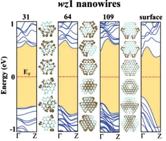
Figure3presents results of the band structure and charge-density analysis performed for wz1 structure. Ideal structure of these wires have Ga-As atom pairs hanging on three sur-faces while other three sursur-faces have the same profile as wz3 type. Upon relaxation these hanging pairs tend to bend to-ward each other, and lower energy by making unusual Ga-Ga and As-As bonds. For example, wz1 structure having 64 atom pairs per unit cell 共wz1–64兲 have four hanging pairs before relaxation. After relaxation first two and last two of them bend to each other, and form a stable structure. wz1 – 31 and wz1 – 109 nanowires have one hanging pair after relax-ation. As a result, all surface atoms of wz1 – 64 structure have coordination number of three while wz1 – 31 and wz1 – 109 have six surface atoms with coordination number of two共see TableI兲. Isosurface charge densities show that three states at
the top of the valence-band edge of wz1 – 64 and wz1 – 109 structures have bulklike character while conduction-band edge states concentrate at the surface. It is hard to define the nature of states in wz1 – 31 structure because it has low di-ameter. To calculate the band structure of the relevant surface we cut a slab from the bulk wurtzite structure parallel to 共011¯0兲 surfaces so that the resulting structure have 11 atomic layers. This slab has two-dimensional periodicity in the sur-face and a vacuum region between adjacent sursur-faces so that they do not interact. The band structure of this slab plotted along k, parallel to关111兴 direction, provide us with
informa-tion about the band structure of nanowires if they were grown thick enough to have a reasonable bulk region in or-der to reduce the corner effects. One expects the band gap of the infinite slab structure to be lower than that of the nano-wires. Comparison of the bands of wz1 – 109 with those of 共011¯0兲 surface confirm their similarity and expected size ef-fect.
Figure 4 shows the band structure and charge-density analysis for wz2 structures. Here all surface atoms of wz2 – 42 and wz2 – 114 structures have coordination number of three while the rest of considered wz2 structures have surface atoms with coordination number of two at the cor-ners. Note that the valence-band edge of wz2 – 42 and wz2 – 114 structures mimic that of infinite slab structure while other structures fail to do that. We see that the band gap of wz2 – 42 is larger than that of wz2 – 114 structure in agreement with the quantum confinement effect. On the other hand, however, wz2 – 25 structure have the lowest band gap. This is caused by large surface-to-volume ratio, which make surface effects pronounced. Isosurface charge densities show that the valence-band edge has bulklike character while conduction-band edge states concentrate on the surface.
FIG. 3. 共Color online兲 Band structure and charge-density isos-urface plots of GaAs nanowires having wz1 structure. Energy band gap between the valence and conduction bands is shaded. Numerals given on top of the bands stand for the number of GaAs atom pairs N in the unit cell. Charge density isosurfaces of specific states at⌫ point are shown on the right-hand side of the bands they belong to. Isosurface charge densities correspond to three valence-band and three conduction-band edge states, ordered in the same manner as bands themselves are. Here we also give the band structure of infi-nite slab of bulk wurtzite structure consisting 11 atomic layers with the same planar 共101¯0兲 surfaces as wz1 nanowires does. Zero of energy is set at the Fermi level EF.
FIG. 4. 共Color online兲 Same as in Fig.3but for wz2 structure. Isosurface charge densities correspond to three valence-band and three conduction-band edge states, ordered in the same manner as bands themselves are.
Band structure and charge-density analysis of wz3 struc-ture is illustrated in Fig. 5. This structure has the largest cohesive energy per atom value compared to other types of nanowires in Fig.1. In this nanowire all surface atoms make three bonds and surface states derived therefrom do not oc-cur in the band gap. Consequently, the band structure of the related infinite slab is very similar to that of wz3 – 96 nano-wire. Charge density of the states at both band edges are spread throughout the nanowire cross section showing the bulk character. Since band gap is not diminished by surface states bands, one can clearly see the quantum confinement effect in these nanowires.
Passivation of dangling bonds of semiconducting nano-wires by hydrogen atoms, generally, results in significant changes in the electronic structure. These changes depend on whether the passivation is done before or after the relaxation of bare nanowires. We find the latter case more suitable for the simulation of the experimental procedure.4 Figure 5 in-cludes information about the effect of hydrogen passivation of all surface dangling bonds on the band structure of wz3 nanowires. In contrast to Si nanowires 共where surface states of bare structure were carried out from forbidden region to the band continua upon passivation with hydrogen兲,4,27,28the band-edge states of wz3 GaAs nanowires remain in their place after the hydrogen saturation. This conclusion is cor-roborated by the analysis of isosurface charge density of states at the center of BZ located at both edges of band gap.
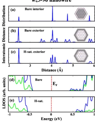
We found that the character and charge distribution of these states do not undergo a change after passivation of surface dangling bonds with hydrogen atoms. Also the similarity in the profile of band edges before and after hydrogen satura-tion is found to be striking. Hydrogen atoms mostly affect the surface states, which, in wz3 structure, are found in the valence-band continua. That is why the effect of hydrogen saturation is not reflected on the band edges in the way it was in silicon nanowires having surface states at the band edges. Here the increase in the band gap occurs not because the edge states are cleared out but because the atomic structure of the nanowires become more bulklike. This effect is illus-trated in Fig. 6, where we analyzed the interatomic distance distribution of wz3 – 96 structure before and after the hydro-gen saturation. Plots given here are done by making a histo-gram of interatomic distances and then smearing it out. The first plot indicates the interatomic distance distribution of the core region of bare nanowire. We get the same result also in the core region of hydrogen saturated structure, and the peaks match the first, second, third, and fourth nearest-neighbor distances of bulk GaAs in wz structure. The crucial difference between bare and hydrogen saturated structures is
FIG. 5. 共Color online兲 Band structure and charge-density isos-urface plots of GaAs nanowires having wz3 structure. Energy band gap between the valence and conduction bands of bare nanowire is 共yellow兲 light shaded. Numerals given on top of the bands stand for the number of GaAs atom pairs N in the unit cell. Charge density isosurfaces of specific states at⌫ point are shown on the right side of the bands they belong to. Isosurface charge densities correspond to three valence-band and three conduction-band edge states, or-dered in the same manner as bands themselves are. Here we also give the band structure of infinite slab of bulk wurtzite structure consisting 11 atomic layers with the same planar共101¯0兲 surfaces as wz3 nanowires does. Zero of energy is set at the Fermi level EF. The widening of the band gap upon the termination of dangling bonds by hydrogen is shown by共green兲 dark-shaded regions delin-eated by black curves at the valence- and conduction-band edges.
FIG. 6. 共Color online兲 Interatomic distance distribution of the core and shell parts of bare and hydrogen saturated wz3 – 96 struc-tures. The ball and stick model illustrates the structure of wz3 – 96 nanowire while the shaded regions defines the core and shell parts of the nanowires. 共a兲 Interatomic distance distribution of interior atoms of bare nanowire. 共b兲 Interatomic distance distribution of exterior atoms of bare nanowires.共c兲 Interatomic distance distribu-tion of hydrogen passivated exterior atoms. 共d兲 Local density of states on surface atoms 共green/light兲 and on the remaining atoms 共blue/dark兲 of bare nanowire. 共e兲 Same as 共d兲 after passivation of surface atoms with hydrogen.
reflected in the shell part of the nanowires. One can clearly see that hydrogen saturated structure have more bulklike character.
Furthermore we performed atom projected density-of-states analysis by calculating the localized density of density-of-states on the surface atoms, as well as on the core atoms before and after passivation with hydrogen atoms. As seen in Figs.6共d兲 and 6共e兲, surface as well as core atoms have comparable contributions to the state distribution at both edges of band gap. These results further corroborate the fact that GaAs nanowires such as wz3 – 96 having surface atoms with coor-dination number of three do not have dangling-bond surface states in the band gap. For nanowires with large D the pas-sivation with hydrogen have negligible effects on the band gap. Note that the increase in the band gap with decreasing diameter holds also for hydrogen saturated structures.
In Fig. 7 we present the band structures and isosurface charge densities of selected states at⌫ point of A wires. Note that we cannot have an infinite slab corresponding to the large A wires because these nanowires have triangular cross section. All relaxed A wires have surface atoms with coordi-nation number of two. The band gap have no obvious trend with varying diameter and is determined by surface states especially falling in the conduction-band edge. For small D the edges of band gap are determined by surface states with low dispersion. As the diameter increases the valence-band edge starts to show bulk character while states at the conduction-band edge remain to display surface character. Even for A − 82 nanowire the flatband states at the edge of the conduction band are located on one of the planar side surface.
The effect of surface states on the band gap is dramatic for the bare GaAs nanowires having zb stacking. The values of band gap as large as 1.5 eV occurring in wz-type nano-wires reduce to the values as small as⬃0.2 eV in zb1-type nanowires. The calculated band gap can even be closed in zb2-type nanowires. It appears that many of the dangling-bond surface states, in particular those associated with the surface atoms having coordination number of two, are placed in the band gap. Therefore one expects dramatic changes in
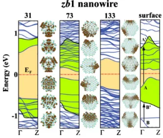
the electronic properties after the passivation of surface dan-gling bonds with hydrogen atoms. The electronic structures of bare zb1-type nanowires are illustrated in Fig.8. Here all surface atoms of zb1 – 31 and zb1 – 113 nanowires have co-ordination number of three after relaxation but certain sur-face atoms of zb1 – 73 structure cannot find a pair to form a bond and stay with coordination number of two. As a result the band gap of zb1 – 73 does not have a value between that of zb1 – 31 and zb1 – 133, as one would expect. To get more information about the nature of the states at both edges of the band gap, we have saturated all dangling bonds of zb1 – 31 and zb1 – 73 structures by hydrogen. After the hydrogen satu-ration the band-edge profile does not stay the same as it was in the case of wz3 structures. This means that the band gap of bare nanowire has increased upon hydrogen passivation of dangling bonds since the band gap is cleared from the sur-face states. Apparently, the band-edge states of the bare zb1 nanowire originate from the surface while in wz3 structure they have bulklike behavior. The different behavior of triply coordinated surface atoms in zb1 and wz3 structure is attrib-uted to their structural orientation. Surface atoms of zb1 structure make atomic rings perpendicular to the wire axis. Dangling bonds of these atomic rings form several mini-bands共with low dispersion along ⌫Z兲 in the band gap, with charge density localized at the surface. Surface atoms of wz3 structure, however, form atomic chains along the wire axis. The dangling bonds of these atomic chains form surface states with high dispersion, which fall in the band continua.
FIG. 7. 共Color online兲 Band structure and charge-density
isos-urface plots for A wires. FIG. 8. 共Color online兲 Band structure and charge-density
isos-urface plots of GaAs nanowires having zb1 structure. Energy band gap between the valence and conduction bands of bare nanowire is 共yellow兲 light shaded. Numerals given on top of the bands stand for the number of GaAs atom pairs N in the unit cell. Charge density isosurfaces of specific states at⌫ point are shown on the right-hand side of the bands they belong to. Isosurface charge densities corre-spond to three valence-band and three conduction-band edge states, ordered in the same manner as bands themselves are. Here we also give the band structure of infinite slab of bulk wurtzite structure with the same planar共112¯兲 surfaces as zb1 nanowires does. Zero of energy is set at the Fermi level EF. The widening of the band gap upon the termination of dangling bonds by hydrogen is shown by 共green兲 dark-shaded regions for N=31, 73, and surface.
The effect of hydrogen saturation is investigated in the case of a slab in Fig.8. Here the first and third valence-band edge states of bare slab structure are labeled as A and B, respec-tively. These dispersive states have bulklike character. Upon the passivation band A rises to A
⬘
forming the conduction-band edge, and conduction-band B rises to B⬘
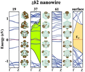
forming the valence-band edge of the passivated structure. Surface states having low dispersion are lowered to valence-band continua.The effects of the dangling-bond surface states are even more dramatic in zb2-type bare GaAs nanowires in Fig. 9, where the band gaps are closed and the nanowires become metallic. Therefore, zb2 type is the only type we have con-sidered to have metallic character. It is interesting that the corresponding infinite slab structure have a finite band gap. zb2 structures would have a band gap which is larger than that of the slab structure if they would had no partly filled corner states crossing the Fermi level. Isosurface charge-density plots support the idea of band-edge states being originated from the dangling bonds at the corners of hexago-nal cross section. We further tested these arguments by pas-sivating the dangling bonds of zb2 – 37 with hydrogen. Upon hydrogen passivation all flat surface-state bands in the range of energy from −0.5 eV to 0.5 eV disappeared and a band gap of 0.9 eV opened. The resulting band profiles near the edges of conduction and valence bands are similar to those of the 共1¯10兲 slab surface given at the right-hand side of Fig.9.
V. DISCUSSIONS AND CONCLUSIONS
We have performed first-principles DFT calculations to reveal the atomic and electronic structures of six different types of bare and hydrogen saturated GaAs nanowires. Nanowires considered have a diameter less than 3 nm, and at this sizes wz3 type have the highest cohesive energy per atom pair while A wires have the lowest. In general, wz nanowires have higher cohesive energy than zb nanowires but the difference in cohesive energies decrease with increas-ing diameter.
We found that all bare GaAs nanowires are semiconduct-ing except zb2 type. In the latter structure, danglsemiconduct-ing-bond states of atoms having coordination number of two cross the Fermi level and hence the structure becomes metallic. For bare GaAs nanowires in wz structure with surface atoms all having coordination number of three, the dangling-bond states associated with these surface atoms do not appear in the band gap but rather in the band continua. Therefore, quantum 共size兲 confinement effect is apparent in their band-gap variation with radius. For these wz-type nanowires the band gap may increase upon the passivation of dangling bonds with hydrogen since bonding of surface atoms become more bulklike.
Surface states of GaAs nanowires in zb structure fall in the band gap, even if all surface atoms have coordination number of three. In wz structure surface atoms form atomic chains along the wire axis while in zb structure they form noninteracting atomic rings perpendicular to the wire axis. Hydrogen saturation dramatically increases the band gap of zb structures by clearing the surface states from the forbid-den region. Generally, increasing diameter results in more bulklike valence-band edge; however conduction-band edge behaves more surfacelike.
For reasons explained in detail, the band-gap variation in GaAs nanowires is rather complex, and depends on their type and geometry, diameter, relaxation, and also whether the dangling bonds of surface atoms are passivated with hydro-gen. We believe that present results are valuable for further research on GaAs and other III–V compound nanowires dealing with their doping, forming heterostructure and mul-tiple quantum well structure, and their fuctionalization to get new electronic and magnetic properties.29,30
ACKNOWLEDGMENTS
Part of the computations have been carried out by using UYBHM at Istanbul Technical University through a grant 共Grant No. 2-024-2007兲.
1See for a recent review of the subject: S. Ciraci, S. Dag, T.
Yildirim, T. Senger, and O. Gulseren, J. Phys.: Condens. Matter 16, R901共2004兲.
2J. Hu, T. W. Odom, and C. M. Lieber, Acc. Chem. Res. 32, 435
共1999兲.
3D. D. D. Ma, C. S. Lee, F. C. K. Au, S. Y. Tong, and S. Lee,
Science 299, 1874共2003兲. FIG. 9. 共Color online兲 Same as in Fig. 8but for zb2 structure.
The shaded region in the band structure of zb2 – 37 corresponds to the band gap opened after the passivation of dangling bonds with hydrogen. zb2 – 19 and zb2 – 61 nanowires are not passivated with hydrogen
4E. Durgun, D. Cakir, N. Akman, and S. Ciraci, Phys. Rev. Lett.
99, 256806共2007兲; E. Durgun, N. Akman, and S. Ciraci, Phys. Rev. B 78, 195116共2008兲.
5L. Esaki and L. L. Chang, Phys. Rev. Lett. 33, 495共1974兲. 6J. C. Harmand, G. Patriarche, N. Péré-Laperne, M.-N.
Mérat-Combes, L. Travers, and F. Glas, Appl. Phys. Lett. 87, 203101 共2005兲.
7S. O. Mariager, C. B. Sørensen, M. Aagesen, J. Nygård, and R.
Feidenhans’l, Appl. Phys. Lett. 91, 083106共2007兲.
8F. Glas, J. C. Harmand, and G. Patriarche, Phys. Rev. Lett. 99,
146101共2007兲.
9V. G. Dubrovskii and N. V. Sibirev, Phys. Rev. B 77, 035414
共2008兲.
10R. Leitsmann and F. Bechstedt, J. Appl. Phys. 102, 063528
共2007兲.
11K. Hiruma, M. Yazawa, K. Haraguchi, and K. Ogawa, J. Appl.
Phys. 74, 3162共1993兲.
12B. J. Ohlsson, M. T. Björk, M. H. Magnusson, K. Deppert, and
L. Samuelson, Appl. Phys. Lett. 79, 3335共2001兲.
13B. A. Wacaser, K. Deppert, L. S. Karlsson, L. Samuelson, and W.
Seifert, J. Cryst. Growth 287, 504共2006兲.
14L. S. Karlsson, K. A. Dick, J. B. Wagner, J. O. Malm, K.
Dep-pert, L. Samuelson, and L. R. Wallenberg, Nanotechnology 18, 485717共2007兲.
15Y. M. Niquet, Phys. Rev. B 74, 155304共2006兲.
16M. P. Persson and H. Q. Xu, Phys. Rev. B 73, 035328共2006兲. 17M. C. Payne, M. P. Teter, D. C. Allen, T. A. Arias, and J. D.
Joannopoulos, Rev. Mod. Phys. 64, 1045共1992兲.
18Numerical computations have been carried out by using VASP
software: G. Kresse and J. Hafner, Phys. Rev. B 47, 558共1993兲; G. Kresse and J. Furthmuller, ibid. 54, 11169共1996兲.
19W. Kohn and L. J. Sham, Phys. Rev. 140, A1133 共1965兲; P.
Hohenberg and W. Kohn, Phys. Rev. 136, B864共1964兲.
20D. Vanderbilt, Phys. Rev. B 41, 7892共1990兲.
21J. P. Perdew, J. A. Chevary, S. H. Vosko, K. A. Jackson, M. R.
Pederson, D. J. Singh, and C. Fiolhais, Phys. Rev. B 46, 6671 共1992兲.
22M. Methfessel and A. T. Paxton, Phys. Rev. B 40, 3616共1989兲. 23H. J. Monkhorst and J. D. Pack, Phys. Rev. B 13, 5188共1976兲. 24P. Sen, O. Gulseren, T. Yildirim, I. P. Batra, and S. Ciraci, Phys.
Rev. B 65, 235433共2002兲.
25R. Rurali and N. Lorente, Phys. Rev. Lett. 94, 026805共2005兲. 26Caution has to be taken in the band-gap values calculated in this
study since DFT underestimates their values. For example, present calculations predict the band gap of bulk GaAs to be only 0.27 eV as compared to the experimental value of 1.4 eV.
27P. W. Leu, B. Shan, and K. Cho, Phys. Rev. B 73, 195320
共2006兲.
28M. Nolan, S. O’Callaghan, G. Fagas, J. C. Greer, and T.
Frauen-heim, Nano Lett. 7, 34共2007兲.
29M. S. Gudiksen, L. J. Lauhon, J. Wang, D. C. Smith, and C. M.
Lieber, Nature共London兲 415, 617 共2002兲.
30M. T. Bjork, B. J. Ohlsson, T. Sass, A. I. Persson, C. Thelander,
M. H. Magnusson, K. Deppert, L. R. Wallenberg, and L. Sam-uelson, Nano Lett. 2, 87共2002兲.