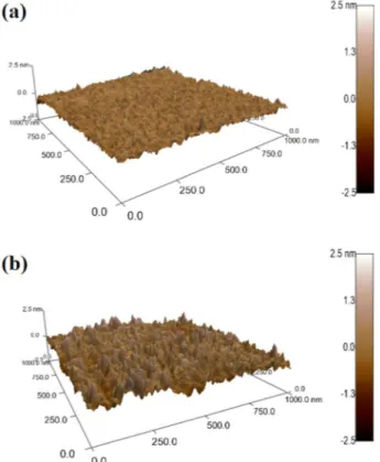
Citation: Journal of Vacuum Science & Technology A: Vacuum, Surfaces, and Films 31, 01A110 (2013); doi: 10.1116/1.4758782
View online: http://dx.doi.org/10.1116/1.4758782
View Table of Contents: http://avs.scitation.org/toc/jva/31/1
Published by the American Vacuum Society
Articles you may be interested in
Gallium oxide (Ga2O3) metal-semiconductor field-effect transistors on single-crystal -Ga2O3 (010) substrates
Applied Physics Letters 100, 013504 (2012); 10.1063/1.3674287
Effect of postdeposition annealing on the electrical properties of β-Ga2O3 thin films grown on p-Si by plasma-enhanced atomic layer deposition
Journal of Vacuum Science & Technology A: Vacuum, Surfaces, and Films 32, 041504 (2014); 10.1116/1.4875935
Structural, electrical, and optical properties of transparent gallium oxide thin films grown by plasma-enhanced atomic layer deposition
Journal of Applied Physics 98, 023504 (2005); 10.1063/1.1980535
Atomic layer deposition of GaN at low temperatures
Journal of Vacuum Science & Technology A: Vacuum, Surfaces, and Films 30, 01A124 (2011); 10.1116/1.3664102
Electronic passivation of silicon surfaces by thin films of atomic layer deposited gallium oxide
Applied Physics Letters 105, 031601 (2014); 10.1063/1.4890737
Effects of post-annealing temperature and oxygen concentration during sputtering on the structural and optical properties of β-Ga2O3 films
Journal of Vacuum Science & Technology A: Vacuum, Surfaces, and Films 34, 060602 (2016); 10.1116/1.4963376
oxygen plasma
Inci Donmez, Cagla Ozgit-Akgun, and Necmi Biyiklia)
UNAM – Institute of Materials Science and Nanotechnology, Bilkent University, 06800 Ankara, Turkey
(Received 1 August 2012; accepted 28 September 2012; published 12 October 2012)
Gallium oxide (Ga2O3) thin films were deposited by plasma-enhanced atomic layer deposition (ALD)
using trimethylgallium as the gallium precursor and oxygen plasma as the oxidant. A wide ALD temperature window was observed from 100 to 400C, where deposition rate was constant at 0.53 A˚ /cycle. X-ray photoelectron spectroscopy survey scans indicated the presence of gallium, oxygen, and carbon elements with concentrations of36, 51.8, and 12.2 at. %, respectively. As-deposited films were amorphous; upon annealing at 900C under N2 atmosphere for 30 min,
polycrystalline b-Ga2O3phase with a monoclinic crystal structure was obtained. Refractive index and
root mean square roughness of the annealed Ga2O3film were higher than those of the as-deposited due to
crystallization.VC 2013 American Vacuum Society. [http://dx.doi.org/10.1116/1.4758782]
I. INTRODUCTION
Gallium oxide (Ga2O3) is a wide band gap material with
good thermal and chemical stability, high dielectric constant, and large band gap (4.9 eV).1,2Combination of these
prop-erties enables Ga2O3thin films to be used in various
applica-tions, including solar cells,3 gas sensors,4 deep-UV photodetectors,5 field-effect transistors,6 and spintronics.7 The growth of Ga2O3films has been accomplished by
tech-niques, such as magnetron sputtering,8electron beam evapo-ration,9pulsed laser deposition,10molecular beam epitaxy,11 metal-organic chemical vapor deposition (MOCVD),12 vapor phase epitaxy,13and sol-gel process.14
Several studies have been reported for the atomic layer dep-osition (ALD) of Ga2O3thin films using different precursors.
First report on the plasma-enhanced ALD (PEALD) of Ga2O3
using oxygen (O2) plasma was published by Shanet al.3Their
study, in which [(CH3)2GaNH2]3was used as the gallium (Ga)
precursor, presented the structural, electrical, and optical prop-erties of the deposited films.15,16Ga2O3and mixed Ga2O3-TiO2
films have also been grown by PEALD using [(CH3)2GaNH2]3
and Ti(NMe2)4 precursors in order to obtain films with large
dielectric constant and low leakage current for electronic device applications.1,17,18 Another study is about the fabrication of metal/insulator/semiconductor capacitors by using Ga2O3as the
insulating layer.19Ga precursor used in this study was not men-tioned by the authors. Besides PEALD, few studies regarding the growth of Ga2O3films using thermal ALD were reported as
well. Dezelah et al.20 employed Ga2(NMe2)6 together with
H2O to obtain Ga2O3 thin films. This process exhibited an
ALD window between 170 and 250C with a growth rate of 1 A˚ /cycle. Recently, Lee et al.21 reported the deposition of Ga2O3thin films via both ALD and MOCVD using a new Ga
precursor, dimethylgallium isopropoxide (Me2GaOiPr). A
nar-row ALD window (280–300C) was reported for the process, and growth rate was found to be 0.28 A˚ /cycle in this region.
In this study, we report on the growth of Ga2O3thin films
using trimethylgallium (TMG) and O2plasma as the Ga source
and oxidant, respectively. To the best of our knowledge,
PEALD of Ga2O3films at such low temperatures using TMG
has not yet been reported. Chemical, structural, and morpholog-ical characterizations of the films are also presented.
II. EXPERIMENT
Ga2O3thin films were deposited by PEALD using TMG as
the Ga precursor and O2plasma as the oxidant. Experiments
were carried out in a Fiji F200 ALD reactor (Cambridge Nanotech) with a base pressure of0.20–0.25 Torr. Solvent-cleaned Si (111) substrates were loaded into the reactor through a load lock. Ga2O3films were then deposited on these
substrates at temperatures starting from room temperature to 400C. Ar was used as the carrier gas with the flow rates of 60 and 200 sccm for TMG and O2, respectively. For the
opti-mization of growth parameters, 150 cycles were deposited at 250C, where one cycle consisted of 0.015 s TMG (precursor bottle temperature 6C)/5 s Ar purge/2–60 s (25 sccm, 300 W) O2 plasma/5 s Ar purge. Postgrowth annealing of
Ga2O3films was performed in a rapid thermal annealing
sys-tem (ATV-Unisys-tem, RTP-1000-150) under 100 sccm N2flow.
Chemical compositions and bonding states of the Ga2O3
thin films were determined by x-ray photoelectron spectros-copy (XPS), using a Thermo Scientific K-Alpha spectrometer equipped with a monochromatic Al Ka x-ray source. Surface morphologies and root mean square (rms) roughnesses of the films were investigated by using an atomic force microscope (AFM, Asylum Research, MFP-3D) in the contact mode. Grazing-incidence x-ray diffraction (GIXRD) measurements were performed in a PANanalytical X’Pert PRO MRD dif-fractometer operating at 45 kV and 40 mA, using Cu Ka radi-ation (k¼ 0.15418 nm). Initial scans were performed within the range of 10–90by using 0.1step size and 0.5 s counting time. For the crystalline samples, additional data were obtained within the same 2h range by the summation of eight scans, which were performed by using 0.1step size and 10 s counting time. Ellipsometric spectra of the Ga2O3 thin film
samples were measured at three angles of incidence (65, 70, and 75) within the wavelength range of 300–1000 nm by spectroscopic ellipsometry (VASE, J. A. Woollam). Cauchy dispersion function was used for modeling the optical a)
estimating the thicknesses of deposited Ga2O3 layers using
the Si/SiO2/Ga2O3model.
III. RESULTS AND DISCUSSION
In order to optimize growth parameters needed for the self-limiting deposition of Ga2O3thin films, effect of TMG dose,
O2 plasma duration, and Ar purge time were studied.
Dou-bling the TMG dose from 0.015 to 0.03 s (precursor bottle temperature6C) did not affect the deposition rate
remark-ably, indicating that 0.015 s is high enough for surface satura-tion. Figure1(a)shows the deposition rate of Ga2O3films as a
Although 10 s was acceptable, 20 s was used for the following Ga2O3depositions. The effect of purge time on growth rate
was also investigated. Five seconds of Ar flow were found to be sufficient for completely purging excess precursors and gaseous byproducts. In order to study the effect of tempera-ture on growth rate, 150 cycles with 0.015 s TMG and 20 s O2
plasma were deposited at different temperatures (28–400C). A wide ALD temperature window was observed from 100 to 400C [Fig. 1(b)], where deposition rate was constant at 0.53 A˚ /cycle. In Fig.1(c), Ga2O3film thicknesses were
plot-ted as a function of the number of PEALD cycles. Films de-posited at 250C exhibited a linear growth behavior. Slope of the linear fit corresponded to deposition rate observed within the ALD window.
Chemical compositions and bonding states of the depos-ited Ga2O3 thin films were studied by XPS. Survey scans
detected peaks of Ga, oxygen (O), and carbon (C) with the concentrations of 36, 51.8, and 12.2 at. %, respec-tively, for the film deposited at 250C. Almost same elemen-tal compositions were measured for the films deposited at different temperatures within the ALD window. The reason of C found in the samples was asserted to be due to surface contamination. To prove this claim, bulk films were reached by applying ion beam etching by using Ar ions with energy of 2 kV. C was not detected in the bulk films obtained by
FIG. 1. Growth rate of Ga2O3thin films as a function of (a) O2plasma flow
duration at 250C, and (b) deposition temperature. TMG dose and O
2
plasma flow rate were constant at 0.015 s and 25 sccm, respectively. (c) Ga2O3film thickness as a function of the number of PEALD cycles.
FIG. 2. (Color online) (a) Ga 3d and (b) O 1s high resolution XPS scans of 26 nm thick Ga2O3thin film deposited at 250C.
60 s etching. Ga 3d high resolution XPS spectrum taken from the surface of 26 nm thick Ga2O3 sample was fitted
by using two subpeaks as shown in Fig.2(a). Subpeak #1, with a binding energy of 21.2 eV, confirmed the presence of Ga–O bond in the samples. Subpeak #2 (25 eV), on the other hand, was related to the contribution from O 2s core level.22 The effect of this contribution on XPS survey scan results is also noteworthy, which leads to an overestimation of the Ga atomic concentration in deposited films. Figure 2(b) is the O 1s high resolution XPS spectrum taken from the sample surface. Binding energy position of the O 1s (532.3 eV) core level was well consistent with the literature.23
Figure 3shows the GIXRD patterns of as-deposited and annealed Ga2O3films. Although these patterns belong to a
film deposited at 250C, PEALD-grown Ga2O3 thin films
were found to be amorphous in the as-deposited state irre-spective of their deposition temperature. Upon annealing at 900C for 30 min under N2 atmosphere, polycrystalline
b-Ga2O3 films with a monoclinic crystal structure were
obtained (ICDD reference code: 00-011-0370). Among all the five different allotropic modifications of Ga2O3, b-Ga2O3
is known to be the most stable and frequent one reported for
thin films.24In order to determine the annealing temperature at which crystallization starts, as-deposited samples were also annealed at 500, 600, 700, and 800C for 30 min under N2atmosphere. GIXRD patterns of these samples indicated
that crystallization starts at 600C. Crystallinity of the b-Ga2O3films increased with annealing temperature.
AFM analyses were performed for revealing the surface morphologies and measuring the rms roughnesses of 26 nm thick Ga2O3thin films deposited on Si (111)
sub-strates. Figures4(a)and4(b)show 3D AFM topographies of the as-deposited and annealed samples, respectively. rms roughness value, which was measured from a 1 lm 1 lm scan area, increased from 0.16 to 0.37 nm after annealing at 900C for 30 min. Increase in the rms roughness value after annealing was attributed to the formation of grains upon crystallization.
Thicknesses and optical constants of Ga2O3 thin films
were estimated by modeling the spectra measured by spec-troscopic ellipsometry within the wavelength range of 300– 1000 nm. Ellipsometric spectra of the as-deposited and annealed Ga2O3thin films (500 PEALD cycles) were
mod-eled by the Cauchy dispersion function using Si (0.5 mm)/ SiO2(1.83 nm)/Ga2O3 layer structure. The thickness of the
as-deposited film was measured as 26.2 nm, which did not change remarkably after postgrowth annealing. Refractive index values, on the other hand, increased from 2.05–1.86 to 2.09–1.92 for 300–1000 nm spectral range (Fig. 5). These results again indicate structural enhancement upon annealing at 900C.
FIG. 3. GIXRD patterns of as-deposited and annealed26 nm thick Ga2O3
thin films. Film deposited at 250C was amorphous in the as-deposited state. GIXRD pattern of the annealed film reveals a polycrystalline structure and corresponds to the b-Ga2O3phase.
FIG. 4. (Color online) 3D surface morphologies of (a) as-deposited (250C) and (b) annealed26 nm thick Ga2O3thin films.
IV. SUMMARY AND CONCLUSIONS
Ga2O3thin films were deposited via PEALD at
tempera-tures starting from room temperature using TMG and O2
plasma. A wide ALD window ranging from 100 to 400C was observed with a constant deposition rate of 0.53 A˚ / cycle. XPS studies confirmed the presence of Ga2O3, and C
detected in the survey scans was attributed to surface con-tamination. Although as-deposited films were amorphous, annealing at 900C for 30 min under N2atmosphere resulted
in crystallization. Upon postgrowth annealing, polycrystal-line b-Ga2O3 thin films with monoclinic structure were
obtained, which also exhibited higher refractive indices and rms roughnesses when compared to their as-deposited counterparts.
ACKNOWLEDGMENTS
This work was performed at UNAM supported by the State Planning Organization (DPT) of Turkey through the National Nanotechnology Research Centre Project. N.B. acknowledges support from Marie Curie International Re-integration Grant (Grant No. PIRG05-GA-2009-249196).
G. X. Liu, F. K. Shan, J. J. Park, W. J. Lee, G. H. Lee, I. S. Kim, B. C. Shin, and S. G. Yoon,J. Electroceram.17, 145 (2006).
2
M. Orita, H. Ohta, M. Hirano, and H. Hosono,Appl. Phys. Lett.77, 4166 (2000).
3
F. K. Shan, G. X. Liu, W. J. Lee, G. H. Lee, and I. S. Kim,J. Appl. Phys.
98, 023504 (2005).
4
M. Ogita, S. Yuasa, K. Kobayashi, Y. Yamada, Y. Nakanishi, and Y. Hatanaka,Appl. Surf. Sci.212–213, 397 (2003).
5S. Fujita,Proc. SPIE
7041, 70410M (2008).
6
M. Higashiwaki, K. Sasaki, A. Kuramata, T. Masui, and S. Yamakoshi,
Appl. Phys. Lett.100, 013504 (2012).
7H. Hayashi, R. Huang, H. Ikeno, F. Oba, and S. Yoshika,Appl. Phys. Lett.
89, 181903 (2006).
8
J. H. Kim and P. H. Holloway,J. Vac. Sci. Technol. A20, 928 (2002).
9
N. C. Oldham, C. J. Hill, C. M. Garland, and T. C. McGill,J. Vac. Sci. Technol. A20, 809 (2002).
10
S.-L. Ou, D.-S. Wuu, Y.-C. Fu, S.-P. Liu, R.-H. Horng, L. Liu, and Z.-C. Feng,Mater. Chem. Phys.133, 700 (2012).
11
M. Holland, C. R. Stanley, W. Reid, R. J. Hill, and D. A. Moran,J. Vac. Sci. Technol. B25, 1706 (2007).
12H. W. Kim and N. H. Kim,Mater. Sci. Eng., B
110, 34 (2004).
13
L. Kong, J. Ma, C. Luan, W. Mi, and Y. Lv,Thin Solid Films520, 4270 (2012).
14Y. Kokubun, K. Miura, F. Endo, and S. Nakagomi,Appl. Phys. Lett.90,
031912 (2007).
15
F. K. Shan, G. X. Liu, W. J. Lee, G. H. Lee, I. S. Kim, and B. C. Shin,
Integr. Ferroelectr.80, 197 (2006).
16G. X. Liu, F. K. Shan, W. J. Lee, B. C. Shin, S. C. Kim, H. S. Kim, and C.
R. Cho,Integr. Ferroelectr.94, 11 (2007).
17
N.-J. Seong, S.-G. Yoon, and W.-J. Lee,Appl. Phys. Lett. 87, 082909 (2005).
18G. X. Liu, F. K. Shan, W. J. Lee, G. H. Lee, I. S. Kim, and B. C. Shin,
Integr. Ferroelectr.85, 155 (2006).
19
S.-A. Lee, J.-Y. Hwang, J.-P. Kim, C.-R. Cho, W.-J. Lee, and S.-Y. Jeong,
J. Korean Phys. Soc.47, S292 (2005).
20C. L. Dezelah IV, J. Niinist€o, K. Arstila, L. Niinisto, and C. H. Winter,
Chem. Mater.18, 471 (2006).
21
H. Lee, K. Kim, J.-J. Woo, D.-J. Jun, Y. Park, Y. Kim, H. W. Lee, Y. J. Cho, and H. M. Cho,Chem. Vap. Deposition17, 191 (2011).
22D. H. Kim, S. H. Yoo, T.-M. Chung, K.-S. An, H.-S. Yoo, and Y. Kim,
Bull. Korean Chem. Soc.23, 225 (2002).
23
V. K. Josepovits, O. Krafcsik, G. Kiss, and I. V. Perczel,Sens. Actuators B48, 373 (1998).
24M. Rebien, W. Henrion, M. Hong, J. P. Mannaerts, and M. Fleischer,
Appl. Phys. Lett.81, 250 (2002). FIG. 5. (Color online) Optical constants of as-deposited (250C) and
annealed26 nm thick Ga2O3thin films.