PROCEEDINGS OF SPIE
SPIEDigitalLibrary.org/conference-proceedings-of-spie
High-speed visible-blind GaN-based
ITO-Schottky photodiodes
Necmi Biyikli
Ibrahim Kimukin
Tolga Kartaloglu
Orhan Aytur
Ekmel Ozbay
High-speed visible-blind GaN-based ITO-Schottky photodiodes
Necmi Biyikli
a, Ibrahim Kimukin
b, Tolga Kartaloglu
a, Orhan Aytur
a, and Ekmel Ozbay
ba
Department of Electrical and Electronics Engineering, Bilkent University, Ankara, Turkey, 06533
bDepartment of Physics, Bilkent University, Ankara, Turkey, 06533
ABSTRACT
In this paper we present our efforts on the design, fabrication and characterization of high-speed, visible-blind, GaN-based ultra-violet (UV) photodiodes using indium-tin-oxide (ITO) Schottky contacts. ITO is known as a transparent conducting material for the visible and near infrared part of the electromagnetic spectrum. We have investigated the optical properties of thin ITO films in the ultraviolet spectrum. The transmission and reflection measurements showed that thin ITO films had better transparencies than thin Au films for wavelengths greater than 280 nm. Using a microwave compatible fabrication process, we have fabricated Au and ITO based Schottky photodiodes on n-/n+ GaN epitaxial layers. We have made current-voltage (I-V), spectral quantum efficiency, and high-speed characterization of the fabricated devices. I-V characterization showed us that the Au-Schottky samples had better electrical characteristics mainly due to the larger Schottky barrier. However, due to the better optical transparency, ITO-Schottky devices exhibited higher quantum efficiencies compared to Au-Schottky devices. ITO-Schottky photodiodes with ~80 nm thick ITO films resulted in a maximum quantum efficiency of 47%, whereas Au-Schottky photodiode samples with ~10 nm thick Au films displayed a maximum efficiency of 27% in the visible-blind spectrum. UV/visible rejection ratios over three orders of magnitude were obtained for both samples. High-frequency characterization of the devices was performed via pulse-response measurements at 360 nm. ITO-Schottky photodiodes showed excellent high-speed characteristics with rise times as small as 12 psec and RC-time constant limited pulse-widths of 60 psec.
Keywords: GaN, photodiode, Schottky, ultraviolet, visible-blind, indium-tin-oxide, quantum efficiency, high-speed
1. INTRODUCTION
Visible/solar-blind photodetectors are essential components for a number of applications including missile-launching detection, flame sensing, ultraviolet (UV) radiation monitoring and secure space-to-space communications. Due to their direct band gap, sharp band-edge cut-off characteristics and good electrical properties, AlxGa1-xN/GaN is the most
promising material system for high-performance UV photodetectors.1 With the advancing growth technology of epitaxial AlxGa1-xN/GaN layers, AlxGa1-xN/GaN-based visible/solar-blind photodiodes (PDs) with excellent detector
performances have been demonstrated by several research groups.2-11 The difficulty of p-type doping of AlxGa1-xN
layers, ease of fabrication and better high-frequency characteristics makes Schottky PDs attractive for high-performance UV photodetection. AlxGa1-xN-based Schottky PDs with different types of thin semi-transparent metal contacts have
been fabricated successfully. Responsivities as high as 0.18 A/W12 and 3-dB bandwidths of 16 GHz13 were obtained with GaN-based Pd-Schottky and Pt-MSM type of PDs respectively.
Due to the very high absorptance of GaN layers, the efficiency performance of GaN Schottky PDs with sufficiently thick (>200 nm) absorption layers is limited by the transmittance of the Schottky contact layer.14 Semitransparent Schottky metal layers are highly absorptive and reflective, and have huge surface roughnesses, all reducing the quantum efficiency of the devices. Indium tin oxide (ITO), which is known as a transparent conductor, has been successfully demonstrated as transparent Schottky-contact material for PDs operating in the visible15,16 and infrared spectrum.17 Both high-quality ITO ohmic18 and Schottky19 contacts to GaN layers were reported. However, to our knowledge visible-blind GaN-based PDs using ITO-Schottky contacts were not reported before. In this paper, we report on the first demonstration of visible-blind ITO-Schottky PDs with RC limited pulse responses. We also compare the performance of our ITO-Schottky PDs with Au-Schottky PDs fabricated on the same wafer.
2. ITO MATERIAL GROWTH AND CHARACTERIZATION
2.1 Material Growth
Before device fabrication, electrical and optical properties of thin ITO films were characterized. The films were deposited in an RF magnetron sputtering system where a composite target containing by weight 90% In2O3 and 10%
SnO2 was used under argon plasma. ITO films were grown with a deposition rate of ~10 nm/min.
2.2 Electrical Characterization
For electrical characterization, a thin ITO film was deposited on a semi-insulating GaAs wafer. Current-voltage measurements were performed using 4 DC probes on a microwave probe-station. Using transmission-line method, the resistivity of the thin ITO film was measured. The resistivity of 100 nm-thick ITO films was determined to be 2x10⁻⁴Ω -cm.
2.3 Optical Characterization
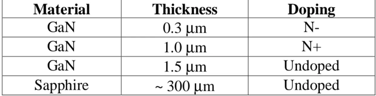
A fiber-optic based UV-optical transmission/reflection measurement setup was used for optical transparency measurements of ITO films sputtered on quartz substrates. The UV-absorption spectrum was determined by measuring the transmittivity and reflectivity of the film and subtracting their sum from 100%. For comparison, a thin Au film was also deposited via thermal evaporation on quartz substrate. The thickness of the Au film was 10 nm, which is the typical Schottky metal thickness used for Schottky PDs.20,21 Figure 1 shows the absorption spectrum of 80 nm thick ITO and 10 nm thick Au films in the 200-500 nm spectral region. The measurement results showed that the ITO film lost its full transparency for wavelengths shorter than 400 nm. However, the 80 nm thick ITO film still exhibited lower absorption than the 10 nm thick semitransparent Au film for λ > 310 nm. For wavelengths near the band gap edge of GaN (λ~360 nm), the ITO film absorbed less than 10% of the incident radiation. These results convinced us that ITO films could be used as low-loss Schottky contacts on GaN layers for visible-blind PD operation.
3. DESIGN
The epitaxial GaN layers of our Schottky PD wafer were grown on a sapphire substrate using metalorganic chemical vapor deposition (MOCVD). First an undoped GaN layer of 1.5 µm thickness was grown which was used as the mesa isolation layer. This was followed by the deposition of a 1.0 µm thick, highly doped (n+ = 2x1018 cm-3) GaN ohmic contact layer. The growth process was completed with a 0.3 µm thick, lightly doped (n = 1x1017 cm-3) active layer. Table 1 shows the epitaxial layer structure of the grown photodiode wafer.
Material Thickness Doping
GaN
0.3
µ
m
N-
GaN
1.0
µ
m
N+
GaN
1.5
µ
m
Undoped
Sapphire
~ 300
µ
m
Undoped
Table 1: Epitaxial layer structure of the grown Schottky photodiode wafer
Proc. SPIE Vol. 4650 76
4. FABRICATION
The samples were fabricated by using a four-step microwave-compatible fabrication process in a class-100 clean room environment. First, the ohmic contacts were defined via reactive ion etching (RIE) under CCl2F2 plasma, 20 sccm gas
flow-rate and 100 W RF power. With an etch rate of ~28 nm/min, an ohmic etch of ~0.6 µm was completed in 22 minutes. Afterwards Ti/Al contacts were deposited using thermal evaporation and standard lift-off process. The contacts were annealed at 450 oC for 45 seconds in a rapid thermal annealing (RTA) system. Mesa structures of the devices were formed via the same RIE process, by etching all the layers down to the undoped mesa isolation layer. Third step was the deposition of the Schottky contact material, where 80 nm thick ITO and 10 nm thick Au films were sputtered and evaporated respectively on two separate samples. ITO film was deposited with a 0.15 nm/sec growth rate, whereas the Au film was evaporated with a rate of 0.1 nm/sec. The ITO films were etched to define the contact regions using dilute HF:H20 solution, whereas the Au films were lifted-off in aceton. Finally, a ~ 0.7 µm thick Ti/Au interconnect metal was
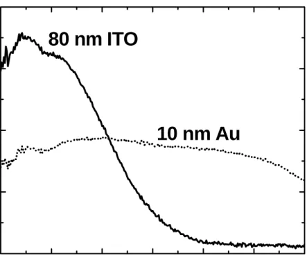
deposited and lifted-off to connect the Schottky layers to coplanar waveguide transmission line pads. Figure 2(a) and 2(b) shows the scanning electron microscope (SEM) photograph and the cross-section schematic of a fabricated ITO-Schottky photodiode.
200
250
300
350
400
450
500
0
20
40
60
80
80 nm ITO
10 nm Au
A
b
s
o
rp
tio
n
(%
)
Wavelength (nm)
(a)
(b)
Figure 2: (a) SEM photograph (b) the cross-section schematic of a fabricated ITO-Schottky photodiode.
Sapphire substrate
AlN Buffer layer
n
+
GaN
Ti/Al
ITO
undoped GaN
n
-
GaN
Inter-
Connect
Metal
Inter-
Connect
Metal
Proc. SPIE Vol. 4650 78
5. DEVICE CHARACTERIZATION
5.1 Electrical characterization
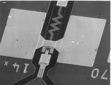
The resulting GaN Schottky PDs had breakdown voltages around 8 V and turn-on voltages around 0.8 V. ITO-Schottky devices displayed leakage currents around 10 nA at 1 V reverse bias for 100 µm diameter devices, mainly due to the low ITO-GaN Schottky barrier height, which was measured as 0.59 eV by forward current-voltage (I-V) measurements (Figure 3). Schottky detectors had better I-V characteristics compared to ITO-Schottky devices. Au-GaN Schottky barrier height was measured as 0.75 eV, which leaded to breakdown voltages larger than 10 V. Dark currents smaller than 1 nA at 1 V reverse bias for 150 µm diameter devices were obtained. The turn-on voltages were around 0.3 V for Au-Schottky PDs. The ideality factors were 1.15 and 1.19 for ITO-Schottky and Au-Schottky samples respectively.
Figure 3: I-V characteristic of a 100 µm diameter ITO-Schottky photodiode.
5.2 Quantum Efficiency Measurements
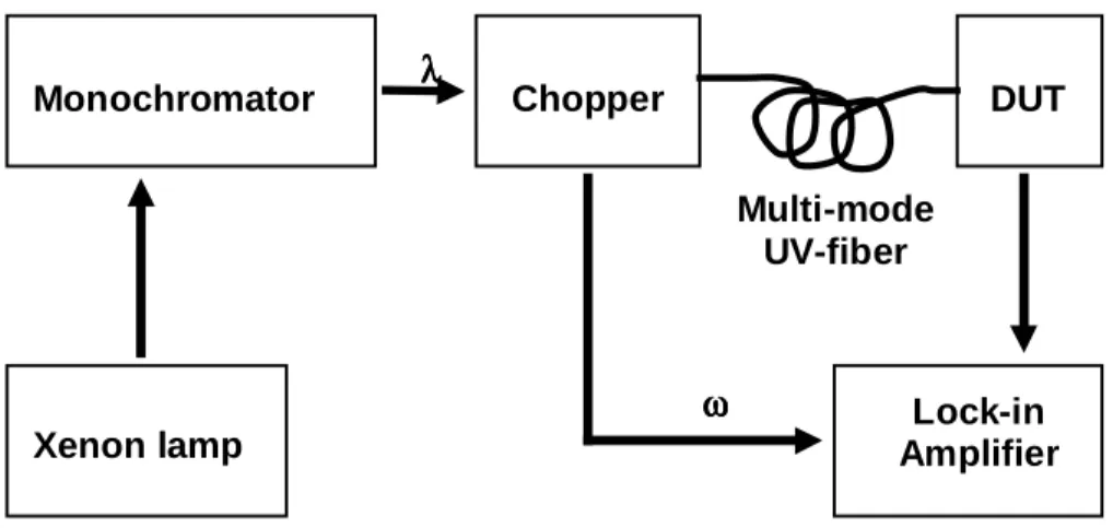
Spectral photoresponse measurements were done in the 250-400 nm range. The experimental setup consisted of a xenon lamp, a monochromator, a multimode UV fiber, a calibrated Si photodetector. The mesurements were performed on a microwave probe station (Figure 4). The xenon lamp was used as the light source, which was coupled into a single-pass monochromator. The monochromated output light was coupled into the multimode UV-fiber by which the samples were illuminated. Calibration of the the light source output was done by using the calibrated Si photodetector. Figure 5 shows the measured spectral quantum efficiency under zero bias in linear scale. ITO-Schottky PD samples showed higher efficiency performance, with efficiency values > 40% in the 290-360 nm region and a maximum efficiency of 47% at 324 nm. As expected, lower efficiency was observed at smaller wavelengths, due to the increased absorption of the ITO film. Au-Schottky PD samples exhibited quite a flat spectral efficiency with a maximum quantum efficiency of 27% around 300 nm. The corresponding device responsivity curves are shown in Figure 6. Peak responsivity values of 0.13
-8
-6
-4
-2
0
2
-1.0
-0.5
0.0
0.5
1.0
Cu
rr
e
n
t (
µµµµ
A)
Voltage (V)
A/W around 350 nm and 0.07 A/W around 310 nm were achieved for ITO-Schottky PD and Au-Schottky PD samples respectively. A UV/visible contrast of more than 3 orders of magnitude was observed in both samples.
Figure 4: Quantum efficiency measurement setup for UV photodiodes.
Figure 5: Measured spectral quantum efficiency of ITO-Schottky PD (solid) and Au-Schottky PD (dotted).
Xenon lamp
Monochromator
Chopper
DUT
Multi-mode
UV-fiber
Lock-in
Amplifier
λλλλ
ω
ω
ω
ω
250
300
350
400
0
10
20
30
40
50
Au: Max = 27% @ 315 nm
ITO: Max = 47% @ 325 nm
Au
ITO
Q
u
an
tum
E
ffi
cie
n
c
y
(%
)
Wavelength (nm)
Proc. SPIE Vol. 4650 80
Figure 6: Measured spectral responsivity curves of ITO-Schottky PD (solid) and Au-Schottky PD (dotted).
5.3 High-speed characterization
Figure 7: Experimental setup used for high-speed characterization of UV photodiodes.
Ti-Sapphire
Mode-locked Laser
BBO Crystal
UV
Lens
Microwave
Probe Station
ω
ω
ω
ω
2ω
2ω
2ω
2ω
718 nm
359 nm
Sampling
Oscilloscope
250
300
350
400
10
-410
-310
-210
-1UV/VIS rejection > 10
3Au
ITO
R
e
sp
on
siv
ity
(A
/W
)
Wavelength (nm)
To characterize the high-frequency response of our ITO-Schottky devices, we have frequency doubled the 718 nm-output of a picosecond mode-locked Ti:sapphire laser using a β-BaB2O4 (BBO) crystal. The outcoming 359 nm
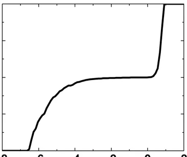
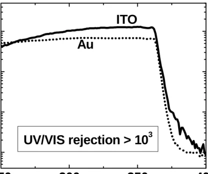
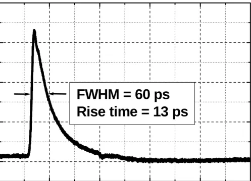
UV-light was focused onto the devices using a UV grade fused silica lens with a focal length of 15 mm. High speed characterization of the detectors was obtained by using a microwave probe station and a 50-GHz sampling scope (Figure 7). The pulse response obtained from a 80 µm diameter device at zero bias, is shown in Figure 8. The detector had a 10%-90% rise time of 13 ps, and a full-width at half-maximum (FWHM) of 60 ps . The decay portion of the pulse response exhibited an RC limited type behavior. By fitting an exponential to the decaying part, we have obtained an RC time constant of 82 ps. This is in good agreement with the calculated RC time constant of 90 ps. The fast Fourier transform of the pulse response yielded a 3-dB bandwidth of 2.6 GHz.
Figure 8: Temporal pulse response of an 80 µm diameter ITO-Schottky PD.
6. CONCLUSION
In summary, we have demonstrated high-speed, visible-blind GaN PDs using ITO Schottky layers. We observed a nearly two-fold enhancement of quantum efficiency compared with semi-transparent Au-Schottky PDs. We achieved a maximum external quantum efficiency of 47% at 325 nm and a peak responsivity of 0.13 A/W at 350 nm. A high-speed performance of 13 ps rise time and 60 ps FWHM was achieved with the fabricated ITO-Schottky PDs.
0
200
400
600
800
1000
0
2
4
6
8
FWHM = 60 ps
Rise time = 13 ps
V
o
ltag
e (m
V
)
Time (psec)
Proc. SPIE Vol. 4650 82
ACKNOWLEDGEMENTS
This work was supported by NATO Grant No. SfP971970, National Science Foundation Grant No. INT-9906220, Turkish Department of Defense Grant No. KOBRA-001 and Thales JP8.04
REFERENCES
1. M. Razeghi and A. Rogalski, “Semiconductor ultraviolet detectors,” J. Appl. Phys. 79, 7433 (1996).
2. E. Monroy, F. Calle, E. Munoz, F. Omnes, and P. Gibart, “AlxGa1 – xN:Si Schottky barrier photodiodes with fast
response and high detectivity,” Appl. Phys. Lett. 73, 2146 (1998).
3. W. Yang, T. Nohova, S. Krishnankutty, R. Torreano, S. McPherson, and H. Marsh, “Back-illuminated GaN/AlGaN heterojunction photodiodes with high quantum efficiency and low noise,” Appl. Phys. Lett. 73, 1086 (1998). 4. E. Monroy, F. Calle, E. Munoz, and F. Omnes, “AlGaN metal–semiconductor–metal photodiodes,” Appl. Phys.
Lett. 74, 3401 (1999).
5. E. Monroy, F. Calle, E. Munoz, B. Beaumont, F. Omnes, and P. Gibart, “High UV/visible contrast photodiodes based on epitaxial lateral overgrown GaN layers,” Electron. Lett., 35, 1488 (1999).
6. T. Li, A. L. Beck, C. Collins, R. D. Dupuis, J. C. Campbell, J. C. Carrano, M. J. Schurman, and I. A. Ferguson, “Improved ultraviolet quantum efficiency using a semitransparent recessed window AlGaN/GaN heterojunction p-i-n photodiode,” Appl. Phys. Lett. 75, 2421 (1999).
7. D. Walker, V. Kumar, K. Mi, P. Sandvik, P. Kung, X. H. Zhang, and M. Razeghi, “Solar-blind AlGaN photodiodes with very low cutoff wavelength,” Appl. Phys. Lett. 76, 403 (2000).
8. E. J. Tarsa, P. Kozodoy, J. Ibbetson, B. P. Keller, G. Parish, and U. Mishra, “Solar-blind AlGaN-based inverted heterostructure photodiodes,” Appl. Phys. Lett. 77, 316 (2000).
9. V. Adivarahan, G. Simin, J. W. Yang, A. Lunev, M. Asif Khan, N. Pala, M. Shur, and R. Gaska, “SiO2-passivated
lateral-geometry GaN transparent Schottky-barrier detectors,” Appl. Phys. Lett. 77, 863 (2000).
10. D. L. Pulfrey, J. J. Kuek, M. P. Leslie, B. D. Nener, G. Parish, U. K. Mishra, P. Kozodoy, and E. J. Tarsa, “High UV/solar rejection ratios in GaN/AlGaN/GaN p-i-n photodiodes,” IEEE Trans. Electron. Devices, 48, 486 (2001). 11. T. Li, D. J. H. Lambert, M. M. Wong, C. J. Collins, B. Yang, A. L. Beck, U. Chowdhury, R. D. Dupuis, and J. C.
Campbell, “Low-noise back-illuminated Al/sub x/Ga/sub 1-x/N-based p-i-n solar-blind ultraviolet photodetectors,” IEEE J. Quantum Electron. 37, 538 (2001).
12. Q. Chen, J. W. Yang, A. Osinsky, S. Gangopadhyay, B. Lim, M. Z. Anwar, M. Asif Khan, D. Kuksenkov, and H. Temkin, “Schottky barrier detectors on GaN for visible–blind ultraviolet detection,” Appl. Phys. Lett. 70, 2277 (1997).
13. J. C. Carrano, T. Li, D. L. Brown, P. A. Grudowski, C. J. Eiting, R. D. Dupuis, and J. C. Campbell, “Very high-speed metal-semiconductor-metal ultraviolet photodetectors fabricated on GaN,” Appl. Phys. Lett. 73, 2405 (1998). 14. E. Monroy, F. Calle, J. L. Pau, F. J. Sanchez, E. Munoz, F. Omnes, B. Beaumont, P. Gibart, “Analysis and
modeling of AlxGa1–xN-based Schottky barrier photodiodes,” J. Appl. Phys. 88, 2081 (2000).
15. D. G. Parker, P. G. Say, and A. M. Hansom, “110 GHz high-efficiency photodiodes fabricated from indium-tin-oxide/GaAs,” Electron. Lett. 23, 527 (1987).
16. N. Biyikli, I. Kimukin, O. Aytur, M. Gokkavas, M. S. Unlu, and E. Ozbay, “45 GHz bandwidth-efficiency resonant cavity enhanced ITO-Schottky photodiodes,” IEEE Photon. Technol. Lett. 13, 705 (2001).
17. W. A. Wohlmuth, J. W. Seo, P. Fay, C. Caneau, and I. Adesida, “A high-speed ITO-InAlAs-InGaAs Schottky-barrier photodetector,” IEEE Photon. Technol. Lett. 9, 1388 (1997).
18. T. Margalith, O. Buchinsky, D. A. Cohen, A. C. Abare, M. Hansen, S. P. DenBaars, and L. A. Coldren, “Indium tin oxide contacts to gallium nitride optoelectronic devices,” Appl. Phys. Lett. 74, 3930 (1999).
19. J. K. Sheu, Y. K. Su, G. C. Chi, M. J. Jou, and C. M. Chang, “Effects of thermal annealing on the indium tin oxide Schottky contacts of n-GaN,” Appl. Phys. Lett. 72, 3317 (1998).
20. E. Ozbay, M. S. Islam, B. M. Onat, M. Gokkavas, O. Aytur, G. Tuttle, E. Towe, R. H. Henderson, and M. S. Unlu, “Fabrication of high-speed resonant cavity enhanced Schottky photodiodes,” IEEE Photon. Technol. Lett. 9, 672 (1997).
21. M. S. Unlu, M. Gokkavas, B. M. Onat, E. ta, E. Ozbay, R. P. Mirin, K. J. Knopp, K. A. Bertness, and D. H. Christensen, “High bandwidth-efficiency resonant cavity enhanced Schottky photodiodes for 800-850 nm wavelength operation,” Appl. Phys. Lett. 72, 2727 (1998).