2D Materials
PAPER • OPEN ACCESS
Graphene based terahertz phase modulators
To cite this article: N Kakenov et al 2018 2D Mater. 5 035018View the article online for updates and enhancements.
Related content
Reconfigurable metamaterials for terahertz wave manipulation
Mohammed R Hashemi, Semih Cakmakyapan and Mona Jarrahi
-A review of metasurfaces: physics and applications
Hou-Tong Chen, Antoinette J Taylor and Nanfang Yu
-Mapping the electrical properties of large-area graphene
Peter Bøggild, David M A Mackenzie, Patrick R Whelan et al.
-© 2018 IOP Publishing Ltd
1. Introduction
Electromagnetic waves (EMW) are described by vector fields which include polarization degree of freedom and spatial distribution of intensity and phase. Dynamic control of these physical quantities provides means of encoding information. Imaging and communication systems rely on the manipulation of light with electrical signals that can either directly control the generation of light at the source or it can indirectly manipulate the light during the propagation through a medium. For visible and infrared light, electrically controlled sources and rich variety of electro-optical controls have already been developed [1, 2]. These techniques enabled the realization of sophisticated optical devices. For long-wavelength light, radio waves and microwaves, the manipulation of the EMW during the propagation is a challenge. For terahertz radiation, this challenge is even more severe due to the requirement of ultrafast electronics and the lack of active materials. Over the past two decades, a significant amount of research have been devoted to develop active devices which control intensity and phase of terahertz radiation [3–9]. Early studies are based on cooled-semiconductor quantum wells whose intersubband absorption falls into terahertz energies [10, 11]. Depletion of electrons from the quantum
wells leads to the reduced absorption and enhanced reflection. Electromagnetic phenomena achieved by metamaterials enhances these interactions. Chen et al demonstrated metamaterial based intensity and phase modulators [12]. Furthermore, these approaches were used to realize THz imaging systems [13].
Recent developments in the field of 2-dimentional crystals provide alternative solutions to control light– matter interaction in a very broad spectrum. Since light–matter interaction is mediated by high mobil-ity electrons, electrostatic tuning of charge densmobil-ity on atomically thin layers facilitates new ways to control light. Especially, graphene is a unique material that provides gate-tunable high mobility carriers at room temperature. Graphene’s linear band structure yield nearly energy independent spectrum which results in a very broad optical activity ranging from visible [14,
15] to microwave frequencies [16].
In a pioneering work by Rodrigues et al, a back-gated graphene transistor was used as a THz intensity modu-lator [17]. They showed that graphene can be used as an alternative low-loss THz active mat erial. However, the back-gated transistor geometry yields limited modula-tion due to insufficient gating (n < 2 × 1012 cm−2 and ΔEF < 200 meV) [17, 18]. To overcome this limitation we have been working on electrolyte gating schemes to achieve much higher charge densities. Electrolyte
gat-N Kakenov et al 035018 2D MATER. © 2018 IOP Publishing Ltd 5 2D Mater. 2DM 2053-1583 10.1088/2053-1583/aabfaa 3
1
8
2D Materials IOP4
May
Graphene based terahertz phase modulators
N Kakenov1 , M S Ergoktas2 , O Balci1 and C Kocabas1,21 Department of Physics, Bilkent University, Ankara, 06800, Turkey
2 School of Materials and National Graphene Institute, University of Manchester, Oxford Rd, Manchester, M13 9PL, United Kingdom E-mail: [email protected]
Keywords: terahertz phase, graphene, quarter wave surface, electrolyte gating, tunable surface impedance, gradient phase surface Supplementary material for this article is available online
Abstract
Electrical control of amplitude and phase of terahertz radiation (THz) is the key technological challenge for high resolution and noninvasive THz imaging. The lack of active materials and devices hinders the realization of these imaging systems. Here, we demonstrate an efficient terahertz phase and amplitude modulation using electrically tunable graphene devices. Our device structure consists of electrolyte-gated graphene placed at quarter wavelength distance from a reflecting metallic surface. In this geometry, graphene operates as a tunable impedance surface which yields electrically controlled reflection phase. Terahertz time domain reflection spectroscopy reveals the voltage controlled phase modulation of π and the reflection modulation of 50 dB. To show the promises
of our approach, we demonstrate a multipixel phase modulator array which operates as a gradient impedance surface.
PAPER
2018
RECEIVED
6 March 2018
ACCEPTED FOR PUBLICATION
20 April 2018
PUBLISHED
4 May 2018
https://doi.org/10.1088/2053-1583/aabfaa
2D Mater. 5 (2018) 035018
Original content from this work may be used under the terms of the Creative Commons Attribution 3.0 licence. Any further distribution of this work must maintain attribution to the author(s) and the title of the work, journal citation and DOI.
OPEN ACCESS
OPEN ACCESS
May 2018 18
N Kakenov et al
ing with ionic liquids in a supercapacitor geometry produces the most efficient gating with Fermi energy shift larger than 1 eV [15, 16, 19, 20]. In our previous works, we showed that graphene supercapacitors can be used to control light from visible to microwave fre-quencies [15, 16, 20, 21]. Although, these devices show significant intensity modulation, they do not yield considerable phase modulation due to atomically thin optical path. In a recent study, passive metamaterials were integrated with gate-tunable graphene devices to achieve intensity and phase modulation in THz [22] and microwave frequencies [23]. Varying the resistance of graphene introduces electrically tunable loss to the metamaterial modulating reflected intensity and phase of THz waves.
2. Methods and results
In this work, we show that without using any metamaterial structure, a planar graphene near a metallic surface can be used as an efficient phase modulator. Using terahertz time domain reflection spectroscopy, we studied the modulation of reflection phase from the active devices. To realize phase modulator structure, we placed gated graphene at quarter-wavelength-distance (λ/4) from a reflecting
metallic surface. In the literature, this type of structure is known as Salisbury screen or the anti-reflection surface where reflecting signal is highly attenuated due to resonant absorption [24–26]. In this way, the phases of two waves, the ones reflected from graphene and metallic surface, have π difference causing destructive
interference. While the reflectivity from metallic surface is constant, the reflectivity of graphene is tunable with the gate voltage [27]. Hence, by varying the conductance of graphene via ionic gating, we were able to modulate both phase and intensity of terahertz beam.
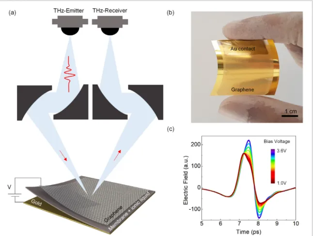
Figure 1(a) shows the schematic representation of the device layout and the THz reflection measurement system. We synthesized large area graphene on cop-per foils using a chemical vapor deposition method and transferred graphene on 20 µm-porous
polyeth-ylene membrane using a photoresist layer (Shipley 1813) as a mechanical support. The Raman spectrum of CVD grown graphene on Si/SiO2 is illustrated in figure S1 of the supporting materials (stacks.iop. org/TDM/5/035018/mmedia). Then, we placed gra-phene coated PE membrane on top of the gold reflec-tor which operates as the gate electrode and the back reflector. The flexibility of the membrane enables us to fabricate bendable phase modulators, figure 1(b).
Figure 1. Electrically tunable phase modulator. (a) Experimental setup used for the terahertz time-domain reflection measurements. THz pulses are generated by InGaAs photoconductive antenna and focused on the device by parabolic mirrors at 10° incidence angle. The phase modulator consists of monolayer graphene on porous 20 µm-thin polyethylene membrane and gold reflector at the back. Ionic liquid electrolyte [deme][Tf2N] is injected into the membrane. (b) Photograph of the fabricated device. (c) Measured time varying electric field of terahertz pulses at gate voltages between 1.0−3.6 V. The THz pulse is suppressed and shifted with varying applied voltage, indicating the phase modulation. Each color represents different gate voltage.
N Kakenov et al
In order to control the charge density on graphene, we soaked an electrolyte ((diethylmethyl(2-meth-oxyethyl) ammonium bis(trifluoromethylsulfonyl) imide, [deme][Tf2N])) into the membrane. Graphene and the gold electrodes form a parallel plate capaci-tor which operates as a tunable THz cavity. By apply-ing small gate voltage between graphene and gold electrodes, we were able to control the charge density (~1014 cm−2) and Fermi energy (>1 eV) of graphene. Figure S2 in the supporting information shows the Fermi energy shift of graphene with respect to applied voltage. We measured the complex THz reflectivity from the device using a time domain terahertz system (Toptica Teraflash System). The system has two fiber-coupled InGaAs antennas which can generate and detect terahertz pulses with >5 THz bandwidth and over 90 dB dynamic range. Using four 1″ parabolic mirrors (Toptica THz reflection head), the terahertz pulse is focused on the sample at 10° incidence angle. Figure 1(c) shows the measured time varying electric field of terahertz pulse at gate voltages from 0 to 2 V. As the gate voltage changes, the reflected THz pulse shows a significant temporal shift with diminishing shape, which also indicates the modulation of the phase and intensity [12, 28, 29].
Fourier transforming the time varying electric field provides the phase and amplitude spectrum. We observed clear multiple resonances in the THz reflec-tion spectrum. The resonance frequency depends on the thickness of the membrane which defines the
cav-ity length, l = λ(2 m + 1)/4n where, n is the index of refraction, λ is the resonance wavelength, and m is
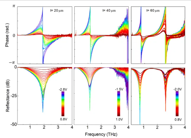
an integer number. Around the resonance, the phase undergoes a π-shift and the reflection intensity shows a suppression of nearly 50 dB. Figure 2 demonstrates the modulation of phase (relative to the phase at Dirac point) and the normalized reflectance spectrum for three devices with cavity lengths 20, 40, and 60 µm.
The color bar indicates the gate voltages varying from charge neutrality point to the highly doped case of gra-phene. The charge neutrality point of graphene occurs at nearly 1 V when it makes contact with ionic liquid medium and gold electrode (figure S3). We observed a clear phase and intensity modulation over a broad spectral range. As the membrane gets thicker, the reso-nance shifts to longer wavelengths due to longer cavity length. We also observed a slight shift in the resonance frequency with the increasing gate voltage.
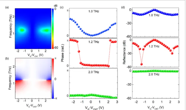
Our device provides efficient means of controlling both intensity and phase of THz waves. Figures 3(a) and (b) show the 2D maps of the THz reflectance and phase as a function of frequency and applied voltage for the 40 µm cavity length device, respectively. The
color scales constitute to the intensity from 0 to 60 dB and phase from π to –π. Two resonance dips occurred at 1.2 THz for negative and positive voltages. The sharp area is indicated in red color for the reflectance val-ues of 50 dB. Nearly perfect electron–hole symmetry in graphene resulted in two resonances for both hole and electron doping. Because of the causal relation the
Figure 2. Phase and amplitude modulation. Variation of phase (radians) and intensity (dB) of the THz reflection of the devices with 20, 40 and 60 µm cavity lengths. The thickness of the membrane defines the cavity length and the resonance frequencies. When the critical coupling condition achieved, the reflectivity is suppressed and the phase shows a step like change around the resonance.
N Kakenov et al
reflection phase and amplitude varies with the gate voltage. The line profile of the phase and reflectance is represented in figures 3(c) and (d) respectively, at frequencies of 1.2, 1.0 and 2.0 THz. These frequen-cies represent three different behaviors; resonance, near-resonance and off-resonance. At the resonance frequency (1.2 THz), the graph shows the π-phase shift
which occurred at positive and negative gate voltages. At near-resonance frequencies (1.0 THz), the reflec-tion phase gradually increases to π/2 at highly doped case. At off-resonance frequencies (2 THz), the phase is nearly constant. Using transfer matrix method we simulated the resonance and off-resonance frequen-cies with respect to surface impedance. The resultant figures are demonstrated in the supporting materials (figure S4). Similarly, in figure 3(d), the intensity vari-ations are depicted for mentioned three cases yielding intensity modulation of 55, 30, 10 dB respectively.
To understand more insight about the operation of the device, we would like to develop a quantitative model using the concept of wave impedance Z = HE where E and H denotes the electric and magnetic field of the wave along the surface. In our device geometry, graphene operates as a tunable impedance surface at THz frequen-cies. Electrostatic control of charge density on graphene yield tunable optical conductivity, σ(ω) which defines
the surface impedance of graphene as Zg = 1+ZZ0σ(ω)0
where Z0 = 377 Ω is the free space impedance and σ (ω) is the frequency dependent optical conductivity of gra-phene. We can describe the tunable optical conductance of graphene with Drude model as,
σ (ω) = σDC
1 − iωτ
where σDC is the DC conductivity of graphene, ω is
angular frequency, and τ is carrier scattering time. Here, the sheet conductivity of graphene, σDC relies
on the Fermi energy σDC = e2
π 2
EFτ [30]. For
microwave frequencies (ω τ−1), the optical
conductivity equals to σDC and the surface impedance
of graphene has only real values. However for THz frequencies, the scattering rate is comparable with the excitation frequency (ω∼ τ−1), hence, resulting in a
complex surface impedance. Note that both σDC and τ
varies with charge concentration.
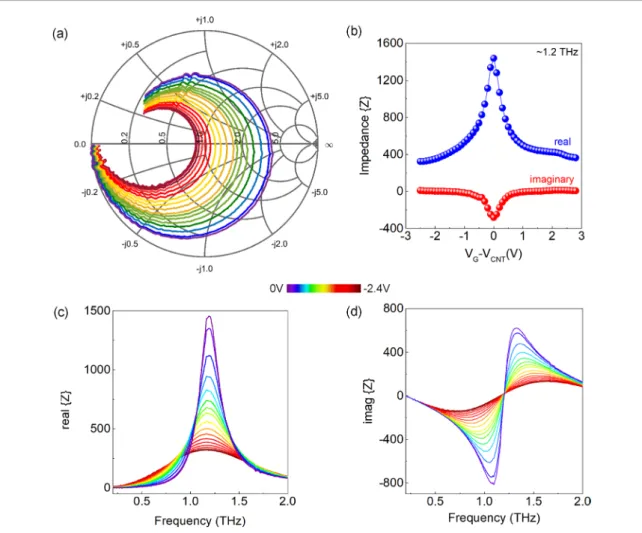
We can extract the surface impedance of the device from time domain terahertz spectroscopy which pro-vides complex Fresnel coefficients. Plotting complex reflectivity in polar coordinates (Smith chart repre-sentation, figure 4(a)) provides wealth of information about the variation of the impedance of the device. The Fresnel coefficient of reflection of the device can be written as r =Z−Z0
Z+Z0. Using this equation, the
sur-face impedance of the device can be extracted from the Smith chart as Z = Z01+ r1− r. Figures 4(b) and (c)
show the extracted real and imaginary parts of the surface impedance at different gate voltages. At the Dirac point, the resistive part of surface imped-ance shows a peak which reaches to a maxima at the resonance frequency. As the gate voltage increases the surface impedance decreases and its spectral distri-bution gets broader. The reactive part of the surface impedance shows undulation from negative to posi-tive values. Around resonance frequencies the imagi-nary impedance is nearly at zero crossing reaching extremum at Dirac point. The variation of the real and imaginary impedance are plotted in figure 4(c). The
Figure 3. Voltage controlled phase. 2D maps showing the variation of the reflection amplitude (a) and the reflection phase (b) as a function of the frequency and the gate voltage. The color bar indicates the values of reflection (dB) and phase (radian). (c) and (d) show the variation of phase and amplitude with the gate voltage for 1.0, 1.2, and 2.0 THz frequencies.
N Kakenov et al
real part of the impedance corresponds to the resist-ance of graphene which changed from 325 Ω to 1450 Ω
with respect to the applied voltage. Unlike microwave frequencies, for THz, the imaginary part of the imped-ance is nonzero effecting the resonimped-ance conditions.
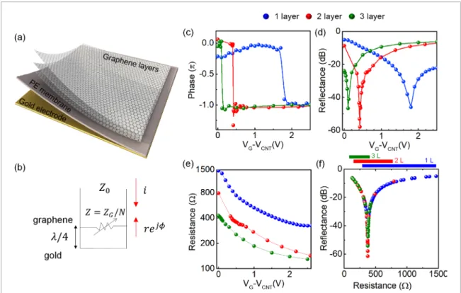
The modulation bandwidth is directly related to the tunability of the resistance of graphene which var-ies between 0.3–1.5 kΩ for single layer. This tunability window is limited by the unintentional doping around Dirac point, and the electrochemical stability of the ionic liquid at high gate voltages. Increasing the num-ber of graphene layers could extend the range of tuna-bility to lower resistance. To test this idea, we fabricated devices with few-layer graphene which were obtained by sequential transfer process of single layer graphene. Figure 5(a) shows the schematic representation of the THz phase modulator with few-layer graphene on 40 µm thick PE membrane. The blue, red, and green
colors correspond to single, two, and tri-layer gra-phene devices, respectively. The small signal model of the device is shown in figure 5(b). The effective surface impedance of the device Z = ZG/N decreases with the
layer number, N. Figures 5(c) and (e) compares the var-iation of THz reflection phase and intensity at 1.2 THz
for single, bilayer and three layer graphene devices. The device with single layer graphene electrode shows the resonance absorption at 1.8 V gate voltage, however, the device with three layer graphene electrode shows the resonance at much lower gate voltage of 0.1 V due to lower resistance. From the reflectivity spectra, we extracted variation of the resist ance of single, two, and three layers graphene with the gate voltage, figure 5(d). At the Dirac point, the maximum resistance is 1500, 800 and 400 Ω respectively. Our experimental results show that graphene layers operate as isolated single layers. We observed linear scaling of the sheet resist-ance with the number of graphene layer. However, similar devices with bilayer graphene synthesized on copper would provide interesting optical response in THz wavelengths due to small electronic band gap. Similarly, at high doping, the minimum resistance for single, bilayer and trilayer graphene are 325, 120 and 100 Ω respectively. Since the resonance condition is governed by the surface impedance of the graphene layer, devices with different layer number show the same scaling behaviors with resist ance, figure 5(f). For all devices, the resonance condition is achieved at nearly Z = 377 Ω. The operational ranges of single,
Figure 4. Tunable impedance surface. (a) Smith chart representation of the complex THz reflectivity which allows us to extract surface impedance of the device. (b) The variation of both the real (x-axis on the chart) and imaginary parts of the impedance at resonance extracted from Smith chart as a function of positive and negative gate voltages. The real (c) and imaginary (d) parts of the complex impedance plotted with respect to frequency.
N Kakenov et al
two, and three layer graphene devices are indicated with respective color, figure 5(f).
We anticipate that the demonstrated phase modu-lation could enable new type of THz devices. To show the promises of our approach, we would like to
demon-strate a multipixel phased array. Figure 6(a) shows the schematic side view of the phased array. We used con-tinuous 3 × 5 cm2 single layer graphene on PE as the top layer. Then we patterned the back electrode (80 nm evaporated gold on flexible substrate) into 1D arrays of
Figure 5. Multilayer phase modulator. (a) Schematic representation of the THz phase modulator using few-layer graphene electrode. (b) Small signal model of the device. Graphene is represented with a variable resistor. The membrane is modeled as a quarter-wave transmission line and the gold reflector is represented with a short circuit at the end of the transmission line. (c) Phase and (d) reflectance modulation of single, two, and three layers of graphene at 1 THz frequency. As the layer number increases, the critical coupling condition (ZD= Z0= 377 Ω) is achieved at lower gate voltages. (e) Extracted sheet resistance of single, two, and three layers of graphene as a function of applied voltage. The minimum resistance for single, bilayer and trilayer graphene are 325, 120 and 100 Ω respectively. (f) Reflectance versus resistance curves for single, two, and three layers of graphene.
Figure 6. Electrically tunable phased-array. (a) Schematic side view of the pixelated phased array which consists of continuous graphene electrodes and patterned gate-electrodes. Individually addressable gold electrodes allows local control of the charge density and the reflection phase. (b) Photograph of fabricated device. (c) Spatial variation of the reflection phase (at 1.1 THz) measured from the multipixel device under different voltage configuration. (d) Corresponding reflectance variations of THz waves at 1.1 THz.
N Kakenov et al
ribbons. Figure 5(b) shows the photograph of the fab-ricated device. We grounded the continuous graphene and applied spatially changing gate voltages to each column. Ability to control the local charge density with the pattered electrodes enable us to generate a phase gradient on the surface. Figure 6(c) shows the meas-ured reflection phase from the pixels at three different voltage configurations for 1.1 THz. In the first case, we applied a gradient voltage to generate a linear spatial phase variation from π/2 to 0 radians. In a similar way, when we reversed the gate voltage by applying consecu-tive 1 V to −3 V from first to last columns, the phase modulation changed from 0 to nearly π/2, respec-tively. In the last configuration, we kept the gate volt-age at zero for all pixels, and the relative phase change was nearly zero radian at 1.1 THz. Figure 6(d) shows the corresponding reflectance variations measured from multipixel device with respect to applied voltages. Using photolithography, the pixel size can be miniatur-ized while extending the density of THz phased-array. A thin film structure can be regarded as a metasurface if the thickness is much smaller than the wavelength [31]. However in our case, the thickness of the device is quarter of the wavelength which is not suitable to classify our structure as a metasurface. In the pixelated device, the lateral dimensions are much longer than the wavelength. It is more suitable to consider these sur-faces as phased arrays. These devices can be regarded as a metadevice when the pixels size is much smaller than the wavelength. We anticipate that scaling the lateral dimension of the pixels to sub wavelength scale would provide new possibility to control not only phase but also polarization state of reflected light.
3. Conclusion
As a conclusion, we demonstrated an efficient THz phase modulator using active graphene devices. Our device comprises electrostatically gated graphene layer placed at quarter-wave distance from a metallic reflector. In this configuration, graphene behaves as a tunable impedance surface modulating reflection phase. At resonance, the phase of terahertz wave undergoes step-like π change while the intensity of the wave is highly attenuated (~50 dB). Efficient carrier density generation at graphene surface is a key parameter that enabled us to modulate the phase of THz radiation. We were also able to extract the complex impedance of electrically gated graphene for THz frequencies. The practicality of device fabrications allowed us to design a tunable phased array on a flexible substrate which operates as a gradient phase surface.
Acknowledgment
This work was supported by the European Research Council (ERC) Consolidator Grant No. ERC-682723
SmartGraphene and CK acknowledges BAGEP Award of the Science Academy.
ORCID iDs
N Kakenov https://orcid.org/0000-0003-2321-6157 M S Ergoktas https://orcid.org/0000-0002-8749-8571 O Balci https://orcid.org/0000-0003-2766-2197 C Kocabas https://orcid.org/0000-0003-0831-5552References
[1] Shields A J 2007 Semiconductor quantum light sources Nat.
Photon. 1215–23
[2] Nowak A K et al 2014 Deterministic and electrically tunable bright single-photon source Nat. Commun. 53240
[3] Unlu M, Hashemi M R, Berry C W, Li S, Yang S H and Jarrahi M 2014 Switchable scattering meta-surfaces for broadband terahertz modulation Sci. Rep. 45708
[4] Shi S F, Zeng B, Han H L, Hong X, Tsai H Z, Jung H S, Zettl A, Crommie M F and Wang F 2015 Optimizing broadband terahertz modulation with hybrid graphene/metasurface structures Nano Lett. 15372–7
[5] Chen H T, Padilla W J, Zide J M O, Gossard A C, Taylor A J and Averitt R D 2006 Active terahertz metamaterial devices Nature 444597–600
[6] Chen H T, O’Hara J F, Taylor A J, Averitt R D, Highstrete C, Lee M and Padilla W J 2007 Complementary planar terahertz metamaterials Opt. Express 151084–95
[7] Kersting R, Strasser G and Unterrainer K 2000 Terahertz phase modulator Electron. Lett. 361156–8
[8] Chen C Y, Hsieh C F, Lin Y F, Pan R P and Pan C L 2004 Magnetically tunable room-temperature 2 pi liquid crystal terahertz phase shifter Opt. Express 122625–30
[9] Lee S H et al 2012 Switching terahertz waves with gate-controlled active graphene metamaterials Nat. Mater. 11936–41
[10] Harrison P, Kelsall R W, Kinsler P and Donovan K 1996 Quantum well intersubband transitions as a source of terahertz radiation Proc. IEEE 6th Int. Conf. on Terahertz
Electronics pp 74–8
[11] Borenstain S I and Katz J 1989 Evaluation of the feasibility of a far-infrared laser based on intersubband transitions in gaas quantum wells Appl. Phys. Lett. 55654–6
[12] Chen H T, Padilla W J, Cich M J, Azad A K, Averitt R D and Taylor A J 2009 A metamaterial solid-state terahertz phase modulator Nat. Photon. 3148–51
[13] Watts C M, Shrekenhamer D, Montoya J, Lipworth G, Hunt J, Sleasman T, Krishna S, Smith D R and Padilla W J 2014 Terahertz compressive imaging with metamaterial spatial light modulators Nat. Photon. 8605–9
[14] Nair R R, Blake P, Grigorenko A N, Novoselov K S, Booth T J, Stauber T, Peres N M R and Geim A K 2008 Fine structure constant defines visual transparency of graphene Science 3201308
[15] Polat E O and Kocabas C 2013 Broadband optical modulators based on graphene supercapacitors Nano Lett. 135851–7
[16] Balci O, Polat E O, Kakenov N and Kocabas C 2015 Graphene-enabled electrically switchable radar-absorbing surfaces Nat.
Commun. 66628
[17] Sensale-Rodriguez B, Yan R S, Kelly M M, Fang T, Tahy K, Hwang W S, Jena D, Liu L and Xing H G 2012 Broadband graphene terahertz modulators enabled by intraband transitions Nat. Commun. 3780
[18] Ren L et al 2012 Terahertz and infrared spectroscopy of gated large-area graphene Nano Lett. 123711–5
N Kakenov et al [19] Kakenov N, Takan T, Ozkan V A, Balci O, Polat E O, Altan H
and Kocabas C 2015 Graphene-enabled electrically controlled terahertz spatial light modulators Opt. Lett. 401984–7
[20] Kakenov N, Balci O, Polat E O, Altan H and Kocabas C 2015 Broadband terahertz modulators using self-gated graphene capacitors J. Opt. Soc. Am. B 321861–6
[21] Kakenov N, Balci O, Takan T, Ozkan V A, Altan H and Kocabas C 2016 Observation of gate-tunable coherent perfect absorption of terahertz radiation in graphene ACS Photonics 31531–5
[22] Miao Z Q, Wu Q, Li X, He Q, Ding K, An Z H, Zhang Y B and Zhou L 2015 Widely tunable terahertz phase modulation with gate-controlled graphene metasurfaces Phys. Rev. X 5
041027
[23] Balci O et al 2018 Electrically switchable metadevices via graphene Sci. Adv. 4eaao1749
[24] Tennant A and Chambers B 2004 Adaptive radar absorbing structure with PIN diode controlled active frequency selective surface Smart Mater. Struct. 13122–5
[25] Woo J M, Kim M S, Kim H W and Jang J H 2014 Graphene based salisbury screen for terahertz absorber Appl. Phys. Lett. 104081106
[26] Jang M S, Brar V W, Sherrott M C, Lopez J J, Kim L, Kim S, Choi M and Atwater H A 2014 Tunable large resonant absorption in a midinfrared graphene Salisbury screen Phys.
Rev. B 90165409
[27] Sensale-Rodriguez B et al 2012 Extraordinary control of terahertz beam reflectance in graphene electro-absorption modulators Nano Lett. 124518–22
[28] Hsieh C F, Pan R P, Tang T T, Chen H L and Pan C L 2006 Voltage-controlled liquid-crystal terahertz phase shifter and quarter-wave plate Opt. Lett. 311112–4
[29] Lin X W, Wu J B, Hu W, Zheng Z G, Wu Z J, Zhu G, Xu F, Jin B B and Lu Y Q 2011 Self-polarizing terahertz liquid crystal phase shifter AIP Adv. 1032133
[30] Liu F L, Chong Y D, Adam S and Polini M 2014 Gate-tunable coherent perfect absorption of terahertz radiation in graphene
2D Mater. 1031001
[31] Yu N and Capasso F 2014 Flat optics with designer metasurfaces Nat. Mater. 13139–50