FEA
TURE AR
TICLE
telecommunications. Conventional opto-electronics relies on high-temperature, gas-phase, epitaxy-grown semiconduc-tors such as III–V compounds,[1,2] which make a mature materials technology. However, high-thermal budget, high-cost, and a limited set of substrates, which are CMOS-incompatible, hamper their use in versatile platforms, including flex-ible surfaces and large-area applications. Besides, the last decade has witnessed the rise of alternative low-dimensional semiconductor materials such as colloidal semiconductor nanocrystals,[3] organic semiconductors[4,5] and more recently, two-dimensional (2D) semiconductors.[6] These materials offer advantages over con-ventional semiconductors thanks to their low cost and low thermal budget growth, solution processability, and roll-to-roll fabrication on arbitrary substrates on a large scale. These materials are expected to impact a broad range of applications in optoelectronics and electronics.
In bulk and weakly confined semicon-ductors, the excited electronic state is typically in the form of free electron–hole pairs due to weak Coulomb interaction energy (∼10 meV).[7] On the other hand, in low-dimensional nanoemitters, the excited state is essentially in the form of strongly bound electron–hole pairs (i.e., excitons) with large Coulomb interaction energy (10 meV) thanks to strong quantum confinement[8] and large dielectric screening,[9,10] allowing for strong light–matter inter-actions. Thus, in these nanoemitters, it becomes central to con-trol excitonic interactions including exciton transfer, diffusion, trapping, dissociation, annihilation, and radiative recombina-tion to accomplish the desired photonic properties and maxi-mize optoelectronic performance.
As it naturally happens in photosynthetic light-harvesting complexes, efficient and directed exciton flow is highly desired in semiconductor nanostructures. To this end, mastering exciton flow at the nanoscale through near-field nonradiative energy transfer has proven vital to accomplish efficient light generation and light utilization using nanoemitters and their hybrid nanostructures.[7,11–15] In this feature article, we high-light recent developments in the field of energy transfer materials for optoelectronics. We review new insights on the near-field nonradiative transfer in excitonic nanoemitter sys-tems. Our main focus is on hybrid systems comprising col-loidal nanocrystals, and 2D and organic semiconductors. Also,
Near-Field Energy Transfer Using Nanoemitters
For Optoelectronics
Burak Guzelturk and Hilmi Volkan Demir*
Effective utilization of excitation energy in nanoemitters requires control of exciton flow at the nanoscale. This can be readily achieved by exploiting near-field nonradiative energy transfer mechanisms such as dipole-dipole coupling (i.e., Förster resonance energy transfer) and simultaneous two-way electron transfer via exchange interaction (i.e., Dexter energy transfer). In this feature article, we review nonradiative energy transfer processes between emerging nanoemitters and exciton scavengers. To this end, we highlight the potential of colloidal semiconductor nanocrystals, organic semiconductors, and two-dimensional materials as efficient exciton scavengers for light harvesting and generation in optoelectronic applications. We present and discuss unprec-edented exciton transfer in nanoemitter–nanostructured semiconductor com-posites enabled by strong light–matter interactions. We elucidate remarkably strong nonradiative energy transfer in self-assembling atomically flat colloidal nanoplatelets. In addition, we underscore the promise of organic semicon-ductor–nanocrystal hybrids for spin-triplet exciton harvesting via Dexter energy transfer. These efficient exciton transferring hybrids will empower desired optoelectronic properties such as long-range exciton diffusion, ultra-fast multiexciton harvesting, and efficient photon upconversion, leading to the development of excitonic optoelectronic devices such as exciton-driven light-emitting diodes, lasers, and photodetectors.
DOI: 10.1002/adfm.201603311 Dr. B. Guzelturk,[+] Prof. H. V. Demir
Department of Electrical and Electronics Engineering Department of Physics
UNAM – Institute of Materials Science and Nanotechnology
Bilkent University Ankara 06800, Turkey
E-mail: [email protected], [email protected]
[+]Present address: Stanford Institute for Materials and Energy Sciences,
SLAC National Accelerator Laboratory, Menlo Park, California, 94025, USA
1. Introduction
Optoelectronics is a key technology that has revolution-ized numerous fields ranging from energy generation to
Prof. H. V. Demir
Luminous! Center of Excellence for Semiconductor Lighting and Displays
School of Electrical and Electronic Engineering School of Physical and Mathematical Sciences School of Materials Science and Engineering Nanyang Technological University
FEA
TURE AR
TICLE
we explore the potential optoelectronic applications of the energy transferring hybrids together with their prospects in sensing and bio-imaging.
2. Nonradiative Energy Transfer Mechanisms:
FRET vs Dexter
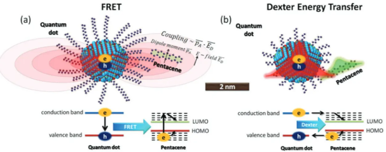
Excitons can be nonradiatively transferred from one molecule to another through near-field interactions such as dipole-dipole coupling and simultaneous two-way electron transfer via exchange interaction, which are known as Förster resonance energy transfer (FRET)[16] and Dexter energy transfer,[17] respec-tively. Figure 1 schematically illustrates these processes between an exemplary donor (e.g., colloidal quantum dot)–acceptor (e.g., pentacene molecule) pair. In these energy transfer processes, the excited donor (D*) relaxes into its ground-state (D) while the excited state energy has been transferred to the acceptor (A*), which was in its ground-state (A) before the transfer occurred. The overall energy transfer process can be repre-sented by D* AkETD A*
+ → + . These processes are called nonradi-ative energy transfers because they do not involve the emission or absorption of a photon.
FRET is a near-field dipole-dipole coupling process where reactive electromagnetic near-field of an oscillating transition dipole in the donor induces a transition dipole in the acceptor (see Figure 1a). Under a weak interaction limit, the FRET rate is directly related to the square of the Coulombic dipole-dipole interaction energy (Eexc)[18]:
kET FRET Eexc pD D pA A d 2 3 2 * *
( )
(
)
≈ = ⋅ → →where kET (FRET) is the FRET rate; pD* D
→ and pA A*
→ are the
transition dipole moments of the D* →D and A →A* transi-tions, respectively; and d is the center-to-center separation distance between the donor and the acceptor. In a more conven-tional form, the FRET rate can be expressed as follows:
kET FRET D D J DA A A f f d 2 6 * κ
(
*)
(
)
≈ → × × →Here, fD*→D and fA A→ * are the oscillator strengths of the
transitions denoted in the subscript, κ2 is the dipole
orien-tation factor, JDA is the spectral overlap integral between the
donor emission and the acceptor absorbance, which implies the existence of energetically resonant states in the acceptor mole cule that match the energy of the excited state in the donor (if D*→ +D hv, then A hv+ →A* should be possible). Also, JDA is a function of fA → A* because it is related to the
extinc-tion coefficient of the acceptor. Thus, the FRET rate necessarily depends on the oscillator strength of both the donor and the acceptor. Because of this, only singlet states, which have non-zero oscillator strength, can be transferred via FRET. One important distinction is that although the FRET rate is directly related to the donor’s decay rate, FRET efficiency is not. FRET efficiency essentially depends on the distance between the donor–acceptor pair and the acceptor’s absorption oscillator
strength. Furthermore, respective orientation of the donor and the acceptor dipoles is important. For randomly oriented dipoles, the dipole orientation factor (κ2) is 2/3, and it reaches
its maximum value of 4 when the transition dipoles are col-linear. For the donors with a photoluminescence quantum yield (QY) less than unity, the FRET rate can be related as follows:
k k k k
QY
decay= rad+ nonrad= rad
kET FRET QY J DA κ
(
)
≈k × × × d decay 2 6Burak Guzelturk received his B.S. (2009), M.S. (2011), and Ph.D. (2016) degrees in the Department of Electrical and Electronics Engineering at Bilkent University. He pursued his Ph.D. under the guidance of Prof. Hilmi Volkan Demir. Currently, he is a postdoctoral research fellow at Stanford University and the SLAC National Accelerator Laboratory in the United States. To date, he has been awarded by the IEEE Photonics Society, the European Technology Platform Photonics21, the German Federal Ministry of Education and Research, and the SPIE for his PhD study. His research interests include understanding excitonic properties in nanoemitters via ultrafast spectros-copy, and tailoring these nanomaterials towards efficient optoelectronics.
Hilmi Volkan Demir received his M.S. and Ph.D. degrees in electrical engineering from Stanford University in 2000 and 2004, respectively. In 2004, he joined Bilkent University as Professor at the Department of Electrical-Electronics Engineering and the Department of Physics. He is the Director of the National Nanotechnology Research Center (UNAM) and the Institute of Materials Science and Nanotechnology at Bilkent University. He is concurrently Nanyang Professor at the School of Electrical Electronic Engineering and Physical and Mathematical Sciences, NTU, and the Director of the LUMINOUS! Center of Excellence for Semiconductor Lighting and Displays. His current research interests include energy-saving LEDs for quality lighting, the science of excitonics for high-efficiency light harvesting, and nanocrystal optoelectronics.
FEA
TURE AR
TICLE
FRET has a distance scaling that intrinsically depends on the geometry of the acceptor. For point-like dipole pairs, the “classic” d−6 scaling factor exists. For one-dimensional (e.g., nanowire), two-dimensional (e.g., quantum well) and three-dimensional (e.g., bulk semiconductor) acceptors, the distance scaling term ranges from d−5, d−4, and d−3, respectively.[19,20] Moreover, a critical distance between donor–acceptor pair is defined, which is commonly known as the Förster radius (R0). FRET efficiency becomes 50% when the donor–acceptor sepa-ration distance is equal to R0, which is expressed as[21]
R QY J N n DA A 9000ln10 128 0 2 5 4 1 6 κ π =
where NA is Avagadro’s number and n is the refractive index.
The Förster radius for typical donor–acceptor pairs is ca. 3–7 nm.[18,21] Recently, longer Förster radii (>10 nm) could be realized by using acceptor materials that have strong light absorption, which is discussed in this feature article. Table 1 highlights effective Förster radii for the recently explored hybrid Figure 1. Schematic illustration of (a) Förster resonance energy transfer (FRET) and (b) Dexter energy transfer. (a) The reactive near-field
electromag-netic field of an oscillating transition dipole in a donor (e.g., CdSe quantum dot) induces a transition dipole in an acceptor (e.g., pentacene). The energy band diagram (below) depicts the resonant transfer of the excitons. (b) A simultaneous electron exchange process (Dexter energy transfer) leads to the transfer of excitons from a donor into an acceptor thanks to the overlapping charge wavefunctions. The energy band diagram highlights Dexter energy transfer that occurs through simultaneous electron exchange interaction.
Table 1. Förster radii for different donor–acceptor pairs commonly consisting of colloidal quantum dots, nanoplatelets, 2D materials, and organic
semiconductors.
Donor Donor emission peak Donor PL QY Acceptor Förster radius (R0)
CdSe/CdS core/shell quantum dot 580 nm N/A Single layer graphene 11.5 nm[22]
Rhodamine dye 650 nm N/A Single layer graphene 15 nm[23]
InGaN quantum well capped with GaN 440 nm N/A Graphene 16 nm[24]
InGaN quantum well capped with GaN 405 nm N/A Graphene oxide 6.4 nm[25]
CdSe/CdS core/shell quantum dot 580 nm 70% Few layer graphene oxide 7.5 nm[26]
CdSe/CdS core/shell quantum dot 620 nm N/A Single layer MoSe2 15.4 nm[27]
CdSe/ZnS core/shell quantum dot 525 nm N/A Single layer SnS2 4–5 nm[28]
CdSe/CdSeS/CdS core/shell quantum dot 605 nm 50% Singe or few layer MoS2 and WS2 5 nm[29]
CdSe/CdZnS core/shell quantum dot 635 nm 80% Single layer MoS2 19 nm
Bulk MoS2 11 nm[30]
4 monolayer (ML) CdSe nanoplatelet 513 nm 30% 4 ML CdSe nanoplatelet 13.5 nm[31]
CdZnS/ZnS core/shell quantum dot 450 nm 38% 4 ML CdSe nanoplatelet 9.5 nm[32]
4 ML CdSe nanoplatelet 513 nm 40% 5 ML CdSe nanoplatelet 10.8 nm[33]
CdSe/ZnS core/shell quantum dot 570 nm 90% Bulk silicon 5.9 nm[34]
Si nanocrystals 627 nm 30% Silicon nanowire 6.2 nm[35]
Polyfluorene 425 nm 50% CdSe/CdZnS/ZnS core/shell quantum dot 5 nm[36]
Alq3 530 nm NA Common organic semiconductors 2–4 nm[37]
FIrpic 480 nm >90% CdSe/CdZnS/ZnS core/shell quantum dot 6 nm[38]
FEA
TURE AR
TICLE
systems such as quantum dot–2D material, quantum dot–nano-platelet, and organic semiconductor–quantum dot.
Dexter energy transfer is the other common near-field non-radiative energy transfer process. Dexter energy transfer relies on the wavefunction (charge orbital) overlap between the donor and the acceptor species. It can be considered as simulta-neous tunneling of electron and hole from the donor into the acceptor. Therefore, for Dexter energy transfer to take place, donor and acceptor molecules should be very close to each other (surface-to-surface separation distance generally ≤1 nm). Also, wavefunction overlap should exist for the orbitals of interacting initial and final states of the electron and hole, respectively.
In Dexter energy transfer, which is a short-range energy transfer process, the transfer rate can be expressed in the form of an exponential decay: k DexterET JDAnormDA e d L ( ) K 2 = × × −
Here kET (Dexter) is the Dexter transfer rate, K is a factor
related to the specific orbital interactions, JDAnorm is the normalized
spectral overlap integral term, d is the center-to-center distance between the donor and the acceptor, and L is the characteristic wave function decay length (e.g., van der Waals radius). JDAnorm
is different from the JDA that is used in the FRET calculation
because the acceptor’s oscillator strength is not important for Dexter energy transfer. Only the normalized absorbance of the acceptor and the normalized emission of the donor are consid-ered to calculate the normalized spectral overlap (JDAnorm), which
should satisfy the resonance condition.
Figure 1b schematically illustrates Dexter energy transfer from an exemplary donor CdSe quantum dot into an exem-plary acceptor pentacene molecule. Organic ligands of the quantum dot are intentionally chosen to be shorter (Figure 1b) to highlight the need for intimate coupling and the wavefunc-tion overlap between the species. Different from FRET, oscil-lator strength of the donor does not play a role in Dexter energy transfer. Therefore, energy transfer from non-emissive tri-plet states become feasible via Dexter energy transfer. Table 2
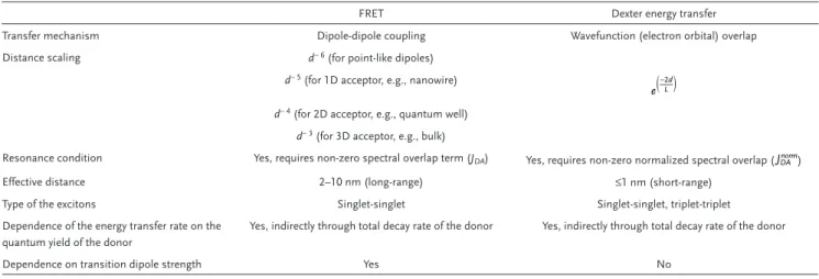
summarizes the similarities and differences between FRET and Dexter energy transfer processes.
3. Exciton Funneling for Light Harvesting
Funneling excitons from a strongly absorbing material into a medium with large electrical conductivity has been estab-lished as a promising strategy to efficiently convert light into electricity.[17,39] Previously, FRET-based exciton funneling schemes[40] were suggested for photosensing and photo voltaics as promising alternatives to photoinduced charge injection- based photosensitization.[41] Charge injection/transfer pro-cesses could only happen for very short separation distances (≤1 nm), thus, FRET-based exciton harvesting, which enable energy transfer at longer distances (≥5 nm), can potentially be more efficient.
In Figure 2a, we illustrate a model light-harvesting nano-structure consisting of a strongly light-absorbing sensitizer (e.g., colloidal quantum dots) that is interfaced with an exciton sink layer (e.g., bulk silicon), which exhibits high electrical con-ductivity. Photogenerated excitons in the sensitizer layer can be transferred to the sink via near-field nonradiative energy transfer. The resonantly transferred excitons contribute to the generation of photocurrent in the sink layer. For this, elec-tron–hole pairs in the sink must be dissociated into free car-riers either by applying an external bias (see Figure 2b) or by creating hetero- or homo-interfaces with staggered band align-ment such as p-n junction (see Figure 2c).
Ideally, sensitizer materials should combine large oscillator strength and high photoluminescence quantum yield together. Commonly, colloidal quantum dots and organic semiconduc-tors have been considered as the sensitizer materials to harvest the photogenerated excitons. As exciton sink layers, mate-rials with high electrical mobility are desired, such as bulk or nanostructured (i.e., quantum wires and wells) semiconduc-tors. Also, 2D semiconductors and colloidal nanoplatelets have recently emerged as promising exciton sinks. Previously, exciton funneling nanostructures have proven to be exciting for photodetectors and photovoltaics.[42–44]
Table 2. Similarities and differences between FRET and Dexter energy transfer processes.
FRET Dexter energy transfer
Transfer mechanism Dipole-dipole coupling Wavefunction (electron orbital) overlap
Distance scaling d− 6 (for point-like dipoles)
d− 5 (for 1D acceptor, e.g., nanowire) 2
e
( )
−Ldd− 4 (for 2D acceptor, e.g., quantum well)
d− 3 (for 3D acceptor, e.g., bulk)
Resonance condition Yes, requires non-zero spectral overlap term (JDA) Yes, requires non-zero normalized spectral overlap (JDAnorm)
Effective distance 2–10 nm (long-range) ≤1 nm (short-range)
Type of the excitons Singlet-singlet Singlet-singlet, triplet-triplet
Dependence of the energy transfer rate on the quantum yield of the donor
Yes, indirectly through total decay rate of the donor Yes, indirectly through total decay rate of the donor
FEA
TURE AR
TICLE
4. Sensitization of Bulk and Nanostructured
Semiconductors
Bulk semiconductors such as silicon and gallium arsenide are typically used for photodetectors and photovoltaics; espe-cially silicon dominates the photovoltaics industry. However, photovoltaic devices, e.g., silicon solar cells, generally suffer from poor spectral utilization of sunlight. For example, UV-blue[45] and NIR-IR[46] portions of the solar spectrum cannot be efficiently converted into electricity by silicon solar cells. To overcome the poor spectral light utilization problem, external sensitization of silicon has been explored via photon down-conversion[46] that can also harness multiple-exciton generation in the nanoemitters.[47] To date, among different sensitization schemes, photon down conversion through radiative energy transfer using light-emitting phosphors has been intensively investigated.[48–50] Notably, nanostructured solar cell architec-tures showed enhanced sensitization thanks to the increased light trapping.[45,51] However, sensitizing silicon through radia-tive energy transfer is inherently restrained due to the limited coupling of the emitted photons to the active medium of the solar cell. Also, multiple radiative recombination and absorp-tion processes lead to significant losses due to intrinsic nonra-diative decay channels in the sensitizer materials.
Alternatively, nonradiative energy transfer could be employed to directly transfer photogenerated electron–hole pairs into bulk and nanostructured semiconductors without emission of a photon by the sensitizer. In the 1970s, Chance, Prock, and Silbey theoretically predicted nonradiative energy transfer into various metals and semiconductors, including silicon and gal-lium arsenide.[52] Alivisatos et al. experimentally demonstrated the spectroscopic evidence of nonradiative energy transfer from an organic molecule pyrene into bulk silicon.[53] Ref. [54] also uncovered nonradiative energy transfer from the organic molecule pyrazine into direct bandgap GaAs. After these early studies, more recently, Madhukar et al. proposed that col-loidal quantum dots would be promising sensitizers for silicon through exciton funneling via nonradiative energy transfer
thanks to their tunable and bright emission, spectrally broad absorption features, and increased environmental stability.[55] In Ref. [55], FRET from near-IR-emitting PbS quantum dots into adjacent InGaAs quantum wells was demonstrated, where the latter acted as an efficient exciton sink and charge transport channel. After this work, Ref. [56] observed FRET from visible-emitting CdSe/CdS quantum dots into GaAs quantum wells, where near-field coupling strength was considerably enhanced by realizing nanohole arrays on the sink material surface. This scheme resulted in 6-fold enhancement of the photocurrent thanks to the intimate integration and the resulting enhanced FRET. Inspired by these works, different quantum dot sen-sitizers and nanostructured semiconductor sinks were also tested. For example, water soluble CdTe quantum dots were integrated with a GaAs quantum well nanohole array, which led to 3-fold photocurrent enhancement.[57] InAs quantum dots were used to enhance photo-transistors of GaAs quantum wells.[58] InGaN quantum wells and CdSe nanowires were also investigated as exciton sinks and charge transport channels when combined with CdSe/ZnS[59] and CdSe/CdS[60] core/shell quantum dots.
To understand the physical origin of the enhanced photo-current in these hybrid systems, Ref. [43] employed time-resolved photocurrent measurements using a hybrid structure consisting of PbS quantum dots decorated on a laterally-patterned silicon substrate. The time-resolved photocurrent measurements strongly suggested the contribution of reso-nantly transferred excitons to the total photocurrent. Further-more, fluorescence spectroscopy measurements on a mon-olayer CdSe/ZnS quantum dot film placed on bulk silicon substrate revealed the efficiency of nonradiative energy transfer into silicon.[34] Considering Förster-like dipole-dipole coupling, near-field energy transfer efficiency was found to be 65% at an effective donor–acceptor distance of 4.4 nm. The resulting effec-tive Förster radius was estimated to be 5.9 nm (see Table 1).
Recently, a temperature-dependent investigation of FRET from a CdSe/ZnS quantum dot film into bulk silicon revealed a strong dependence on the temperature.[61] In this quantum Figure 2. (a) A hybrid platform for exciton funneling from a sensitizer layer (e.g., colloidal quantum dots) into an exciton sink layer (e.g., silicon). The
sensitizer has strong and broadband light absorption and the sink layer possesses good electrical conductivity. Strategies for photocurrent generation in exciton-transferring sensitizer-sink structures: (b) applying external electric field and (c) creating interfaces with staggered band alignment, i.e., p-n junction.
FEA
TURE AR
TICLE
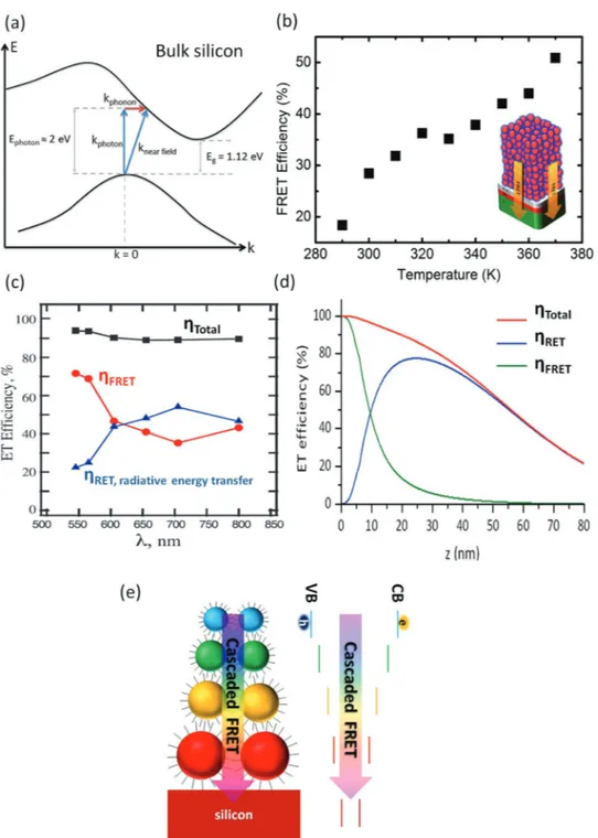
dot–silicon hybrid, FRET efficiencies and rates were observed to be considerably decreased at cryogenic temperatures com-pared to those at room temperature. Previously, in the case of quantum dot-based donors, FRET efficiency has been found to be typically constant as a function of temperature.[62,63] Dif-ferent from previously studied quantum dot donor–direct bandgap acceptor systems, when silicon was used as an acceptor material, the observed strong temperature dependency of the FRET efficiency originated mainly from a highly tem-perature-dependent absorption cross-section of silicon. Since light absorption is a phonon-assisted process (see Figure 3a), the absorption cross-section of silicon is considerably reduced as the temperature is decreased. Furthermore, the temperature-dependent photoluminescence quantum yield of the quantum dots also played a role in the observed changes in the kinetics.
Previously, Dexter et al. predicted that FRET into an indirect bandgap semiconductor could be made more efficient, if the dipole emitter would be placed very close to the surface of the acceptor. This would arise since the wave vector of the dipole near-field (knear field= h/d) would be much larger than the wave
vector of the emitted photon in the far field (kphoton=h/ )λ since d λ, where h is Planck’s constant, d is the separation dis-tance, and λ is the wavelength of light.[64] Therefore, as shown in Figure 3a, nonvertical excitation via FRET into an indirect bandgap could be possible thanks to the large wave vector of the dipole near-field (knearfield). However, the separation distance should be ≤2 nm to realize a near-field wave vector that can cover a significant portion of the Brillouin zone of the indirect bandgap semiconductor (e.g., silicon).[53] In the case of CdSe/ ZnS quantum dots, the separation distance was larger than 4 nm considering the radius of the quantum dots, organic cap-ping ligands, and the native oxide layer. Because of this, in the quantum dot–silicon hybrid, FRET essentially required the assistance of phonons.[61] More importantly, we realized that when the temperature was increased to above room tempera-ture (290 to 370 K), FRET efficiency increased by more than 2-fold (see Figure 3b). This has been attributed to increased absorption in silicon at elevated temperatures due to stronger assistance of phonons and elongated exciton diffusion length in the quantum dot film, leading to a stronger FRET overall.
In addition to FRET, directed radiative energy transfer (RET) has been identified as an efficient way to boost light-harvesting in quantum dot–silicon hybrids. Since FRET is a near-field energy transfer process, its interaction range is quite limited. Therefore, using FRET, one could only efficiently transfer exci-tons that are formed in the closest quantum dot monolayer on top of silicon. To this end, Ref. [65] proposed to use ultrathin silicon nanomembranes (thickness ≈ 100–200 nm) that exhibit photonic waveguiding modes, in which radiative emission of the quantum dots could couple effectively. Following this work, Ref. [66] showed that efficiencies of FRET and RET are highly sensitive to the emission wavelength of the sensitizing quantum dot due to the dispersion of the complex dielectric function of silicon. For the quantum dots emitting in the blue-yellow spec-tral range (λ < 600 nmem ), FRET is stronger than RET. On the
other hand, RET becomes stronger for the quantum dots emit-ting in the near-IR spectral range due to the small absorption cross-section of silicon that limits the dipole-dipole coupling strength. Figure 3c compares the calculated efficiencies of FRET
and RET as a function of the peak emission wavelength of the quantum dots. Total energy transfer efficiency (FRET+RET) is also plotted on the same graph. Although FRET and RET have different efficiencies as a function of the nanoemitter’s emis-sion wavelength, the total energy transfer efficiency is almost constant (∼90%) for a monolayer of quantum dots on top of silicon. This suggests that although near-IR-emitting quantum dots could not be efficient FRET donors for silicon, RET could dominate the overall energy transfer. Therefore, RET could be highly advantageous for light-harvesting devices in addition to FRET.
Recently, several reports realized light sensors[67] and photovoltaic devices[35,68] using quantum dot–silicon hybrids that exhibited enhanced quantum efficiencies thanks to the effi-cient energy flow from the quantum dot sensitizers into silicon. Ref. [67] reported an almost two orders of magnitude enhance-ment of the photocurrent in a back-gated silicon membrane field-effect photo-transistor. FRET and RET were found to par-tially contribute to this large enhancement. Other factors such as change of the electrostatic potential of the channel surface and forward biasing of the metal–semiconductor junction due to exciton transfer were also found to play crucial roles.
Recently, Ref. [68] demonstrated ultrathin hybrid silicon solar cells (thickness ≈ 500 nm) that exhibited power conver-sion efficiency of 1.60% when integrated with a 32 nm-thick quantum dot sensitizer layer (corresponding to four quantum dot monolayers). The power conversion efficiency was 1.08% in the reference device that did not deploy a quantum dot sen-sitizer layer. Contribution of the energy transfer mechanisms (FRET and RET) to the enhanced photovoltaic performance was carefully assessed. Interestingly, the dominant contribution (50%) was found to arise from the optical impedance matching, which arose due to the quantum dot layer acting as a graded refractive index layer between air and silicon. Contributions of FRET and RET to efficiency enhancement were found to be 13% and 37%, respectively.[68] Since the quantum dot layer thickness was relatively large, RET was more effective than FRET. Figure 3d depicts the calculated relative efficiencies of FRET and RET as a function of the separation distance between a monolayer quantum dot and silicon surface. Although FRET is dominant for short distances (<10 nm), RET is dominant larger separation distances.
Although photovoltaic performance could be enhanced by near-field energy transfer, one significant limitation to the device performance is the surface and bulk carrier recom-bination in poorly passivated silicon films. Since resonantly transferred electron–hole pairs in silicon are generated very close to the surface, these pairs could be easily lost due to effective nonradiative surface recombination processes. Thus, there is a strong need to employ well-passivated silicon sur-faces to harvest the transferred electron–hole pairs more effi-ciently. Recently, Ref. [35] demonstrated a buried all-silicon solar cell architecture, which employed a low-temperature UV-ozone treated n-type silicon nanowire array buried in a p-type silicon matrix. These solar cells exhibited consid-erable suppression of the surface and bulk recombination processes.[69] By decorating these silicon solar cells with fluo-rescent silicon nanocrystals, power conversion efficiencies as high as 12.9% were achieved with 20% enhancement as
FEA
TURE AR
TICLE
compared to the reference devices that did not incorporate any nanocrystal FRET-sensitizers. Suppression of the surface recombination in silicon allowed for the effective utilization of the transferred excitons. The enhancement was attributed
to the near-field energy transfer from silicon nanocrystals into silicon nanowires. However, contributions of FRET and RET were not separately evaluated in these highly efficient photo-voltaic devices.
Figure 3. (a) Energy band diagram of bulk silicon. Optical absorption is phonon-assisted due to the indirect bandgap nature (kphoton + kphonon). Large wave vector of dipole near-field (knear field) of a nanoemitter on the surface of silicon could overcome the need for phonon assistance. (b) Temperature-dependent FRET efficiencies into silicon from few-layer-thick CdSe/ZnS quantum dots. Reproduced with permission.[61] Copyright 2013, American
Chemical Society. (c) Efficiency of FRET, directed radiative energy transfer (RET) and total energy transfer (FRET+RET) for monolayer quantum dot films on silicon emitting at different spectral positions ranging from 550–800 nm. Reproduced with permission.[66] Copyright 2013, American Chemical
Society. (d) FRET and RET efficiency for a quantum dot monolayer as a function of separation distance between the quantum dot layer and the silicon surface. Reproduced with permission.[68] Copyright 2015, Royal Society of Chemistry. (e) Rainbow-like graded energy flow structure for multilayered
FEA
TURE AR
TICLE
Another significant limitation of nonradiative energy transfer sensitization of silicon has been the utilization of single- or few-monolayer quantum dot layers. Considering the absorption cross-section of the conventional quantum dots (104–105 cm−1),[70,71] thin quantum layers (≈10 nm) would lead to only ≈10% light absorption. Thus, thicker sensitizer layers (≈100 nm) are needed for efficient light-harvesting. However, excitons generated in the quantum dots that are away from the silicon surface cannot be effectively harvested using single bandgap quantum dots. This is because the excitons in the quantum dot film created further away from silicon cannot be easily transported towards silicon due to the limited exciton diffusion in quantum dot solids (typically 10–20 nm).[72,73] To this end, use of graded energy gap quantum dot assem-blies to funnel the excitons towards the silicon surfaces offers exciting possibilities. Figure 3e illustrates an exemplary graded gap quantum dot sensitizer layer that can achieve directed exciton flow towards the silicon surface. In our recent work, by employing a cascaded energy flow structure (green-emit-ting quantum dot/red-emit(green-emit-ting quantum dot/silicon), we achieved more than 1.5-fold enhancement in the generation of electron–hole pairs in silicon as compared to bilayer control samples without energy gradient (red-emitting quantum dot/ red-emitting quantum dot/silicon and green-emitting quantum dot/green-emitting quantum dot/silicon).[74] Later, Ref. [75] also investigated the potential of cascaded energy transfer using CdSe/ZnS quantum dots into silicon, where they could achieve FRET efficiencies reaching 90%. Previously, rainbow-like energy graded structure quantum dots were also employed for exciton-recycling[76] and light-harvesting in hybrid solar cells.[77–79]
5. Two-Dimensional Materials as Efficient
Exciton Sinks
Two-dimensional materials, the so-called van der Waals mate-rials, have recently emerged as highly promising for nano-electronics,[6,80,81] optoelectronics,[82–84] and bio-sensing.[85,86] Although 2D materials offer large electrical mobility and strong light–matter interactions,[80,82] these materials are restricted by limited overall light absorption due to their ultrathin thick-nesses (one to few monolayers). However, the absorption cross-section is very large in 2D materials. For example, a single layer graphene can absorb 2.3% of the light over a large spectrum (UV to IR), suggesting its huge absorption cross-section. To this end, sensitization of 2D materials by near-field energy transfer from adjacent nanoemitters has attracted increasing attention lately.[22,23,27,28,30,87–92] Recent studies unveiled new physical insights on the near-field energy transfer and realized ultraef-ficient light-harvesting devices using 2D materials hybridized with nanoemitters.
Graphene was the first 2D material to be investigated as exciton sink from nearby nanoemitters via nonradiative energy transfer.[23,87,90,93] Later, graphene derivatives such as gra-phene oxide[26,94,95] and reduced graphene oxide,[26] as well as amorphous carbon layers[96] and carbon nanotubes,[97] were considered for their capability as exciton accepting media for light-harvesting and bio-sensing applications. More recently,
transition metal dichalcogenide (TMDC) monolayers were also investigated, such as MoS2,[30,88,91] MoSe2,[27] WS2,[29] and SnS2,[28] exhibiting strong exciton sinking capability comparable to that of graphene. As exciton-donating nanoemitters, colloidal semiconductor nanocrystals,[22,30,87] nitrogen vacancy centers in diamond,[98] and fluorescent dyes[99] were typically employed. Here, we will focus more on the 2D material–nanocrystal hybrids and their prevailing photophysical properties, which make them exciting for numerous applications.
CdSe/ZnS core/shell quantum dots that were deposited on top of a single-layer graphene exhibited strong photolumi-nescence quenching (∼70-fold).[87] This quenching was well accounted for by strong near-field dipole coupling (i.e., FRET) into graphene. Also, the possibility of charge transfer leading to exciton dissociation at the graphene/quantum dot interface was ruled out due to the relatively thick shell of the quantum dots, which was shown to impede charge transfer.[100] Using fluores-cent dyes in a polymer matrix on top of a single-layer graphene, a more than 90-fold increase in the fluorescence decay rate was reported, when the fluorescent dye is effectively 5 nm away from the graphene sheet.[23] These early experimental reports suggested very strong exciton sink capability of graphene. Also, the effective Förster radius for graphene as an acceptor was estimated to be 11–16 nm[22–24] (see Table 1). Thus, with exceptionally large Förster radius, graphene can empower long range (>20 nm) exciton transfer. This property of graphene has been attributed to its large absorption cross-section (>105 cm−1). Although absolute absorption level of graphene is low (2.3% over the visible and IR spectral region), its cross-section is large when considering graphene’s only single-atom thickness. Furthermore, the gapless nature of graphene allows for fre-quency-independent efficient interband transitions, therefore making it an exciting candidate for an extremely broad range of nanoemitters.
TMDC monolayers were also investigated for their exciton sinking properties. For example, MoS2 led to strong modifica-tion of the fluorescence decay and large photoluminescence quenching of the nearby emitters, which were CdSe/CdZnS quantum dots.[30] The dominant near-field interaction mecha-nism was found to be FRET, as understood by the sensitivity of the process to the spectral overlap between the emission of the quantum dots and the excitonic absorption of the MoS2 mono-layer.[30] An effective Förster radius of 19 nm was estimated for the MoS2 acceptor when using a nanoemitter with a bandgap of ∼2 eV. Yet, the Förster radius for an MoS2 acceptor is highly sensitive to the emission color of the donor since the absorption spectrum of MoS2 exhibits sharp excitonic absorption peaks at around 620 and 660 nm. Thus, the spectral overlap term can be easily altered by using donors emitting at different spectral range. Also, monolayer MoSe2 was studied and shown to have large Förster radius (∼15 nm), similar to that of monolayer MoS2.[27] Strong dipole-dipole coupling and a large interaction range in TMDC monolayers, similar to graphene, have been attributed to strong light–matter interactions in these materials. As compared to their bulk counterparts, which commonly have an indirect bandgap, TMDC monolayers have a direct bandgap with large oscillator strength. Ref. [28] studied exciton transfer into a monolayer SnS2 from colloidal quantum dots. Different from TMDCs, monolayer SnS2 still has an indirect bandgap;
FEA
TURE AR
TICLE
thus, it has limited light absorption. In a monolayer SnS2– quantum dot hybrid, the Förster radius was estimated to be ca. 5 nm, suggesting its inferior exciton sink capability compared to the TMDCs and graphene.
Distance scaling of FRET into 2D materials has been a sub-ject of interest. Theoretical studies have predicted d−4 depend-ence due to the thin, planar nature of the acceptor.[20,93,101] Lately, several experimental studies suggested strong evidence for d−4 distance scaling,[22,23,27] confirming theoretical expecta-tions. These studies employed time-resolved and steady-state fluorescence spectroscopy to assess fluorescence decay rates and steady-state photoluminescence quenching factors as a function of the donor–acceptor separation distance. Smooth dielectric layers such as MgO,[22] TiO
2,[23] HfO2,[26] PMMA,[102] and h-BN[27] were employed to controllably tune the separa-tion distance. Recently, Berciaud et al. compared the distance scaling of FRET into a single-layer graphene from spherical-like colloidal quantum dots and plate-like colloidal quantum wells. For a quantum dot donor, the FRET rate was found to scale with a d−4 distance dependence (see Figure 4a). In the case of col-loidal quantum well donors, a slight deviation from d−4 scaling was observed at short distances, which has been attributed to the larger lateral extent of the free excitons in the nanoplatelets, leading to a deviation from classical dipole emitter approxima-tion.[22] Few studies reported different distance dependencies such as d−2.5[30] and d−2.[24,25] However, these unexpected scaling
terms could simply arise due to the unexpected experimental conditions (e.g., non-smooth spacer layers) or potential charge transfer pathways.
One noteworthy difference between graphene and MoS2 was found on their dependence of energy transfer efficiency and rate as a function of their layer thicknesses. Prins et al. reported that as the number of MoS2 layers increases, FRET becomes less efficient. In contrast, Ref. [87] demonstrated that FRET into graphene becomes stronger as the graphene layer thickness is increased. A recent study compared FRET kinetics in both graphene and MoS2 as a function of layer thicknesses using the same donor (CdSe/ZnS quantum dots emitting at 2.1 eV). Figure 4b shows the photoluminescence decay life-time of the quantum dots on bare SiO2 (dashed line), MoS2/ SiO2 (red triangles), and graphene/SiO2 (blue squares) samples, where the layer thickness of the 2D materials was varied from 1 to 25 monolayers. The intrinsic photoluminescence decay lifetime of the quantum dots on bare SiO2 was measured to be ≈5 ns. When the same quantum dots are on either single-layer MoS2 or single-layer graphene, the photoluminescence lifetime becomes considerably shorter (300 ps) due to efficient FRET into the 2D materials as reported earlier. Interestingly, as the layer thickness of MoS2 is increased, the photolumines-cence lifetime of the quantum dots is observed to elongate, suggesting that the FRET efficiency decreases. In contrast, the photoluminescence lifetime of the donor becomes shorter as
Figure 4. (a) Distance scaling of FRET rate into single layer from graphene CdSe/CdS quantum dot. FRET rate into graphene scales with d−4, where
d is the separation distance between graphene and quantum dot controlled by the thickness of dielectric spacer (MgO). Reproduced with
permis-sion.[22] Copyright 2015, American Chemical Society. (b) Photoluminescence lifetime of the CdSe/ZnS quantum dot donor on MoS
2 (red triangles)
and graphene (blue squares) as a function of the 2D layer thickness. As MoS2 layer thickness increases, decay lifetime of the quantum dots becomes
longer, suggesting the suppression of FRET. As graphene layer thickness increases, decay lifetime of the quantum dots become shorter, suggesting that FRET grows stronger. The dashed line indicates the decay lifetime of the quantum dots on the bare SiO2 layer. (c) Near-field electric field
distribu-tion in single-layer and tri-layer MoS2, and bilayer graphene due to an oscillating transition dipole (i.e., quantum dot). Reproduced with permission:[88]
FEA
TURE AR
TICLE
the number of graphene layers is increased, suggesting that FRET efficiency effectively increases.
To understand and explain the observed differences between MoS2 and graphene, classical CPS (Chance, Prock, and Silbey) theory[52] was employed, which revealed that screening effects are strikingly different between graphene and MoS2 due to the considerable difference of their complex dielectric functions. MoS2 is a highly polarizable material due to its large dielectric constant. Thus, as the layer thickness is increased, the elec-tric field strength at the top MoS2 layer (which is closest to the nanoemitters) is strongly reduced (see Figure 4c) compared to a single-layer MoS2. In contrast, screening effect is not domi-nant for graphene due to its smaller real permittivity. Thus, increasing the layer thickness of graphene leads to a stronger absorption; in turn, this results in increased FRET rates. Overall, acceptor materials with less relative polarizability (e.g., graphene, GaSe and silicon) are expected to exhibit increasing FRET rates as the material thickness is increased. On the other hand, materials such as MoS2, WS2, and InAs will show FRET that becomes weaker as the layer thickness is increased.[88] Fur-thermore, Gartstein et al. theoretically investigated and com-pared both macroscopic analyses by considering an acceptor slab having a complex dielectric function (i.e., CPS theory) and direct modeling, which considered discrete acceptor layers as polarizable point dipoles.[101,103] In both models, non-additivity (non-monotonic behavior) in FRET efficiencies is observed as a function of the acceptor layer thickness, especially when the polarizability of the acceptor layer is relatively high (e.g., ε′ > 7 and ε″ = 0.2). Overall, counter-intuitive trends observed in the nonradiative energy transfer efficiencies as a function of the 2D acceptor materials layer thicknesses can be accounted for by the electric field screening effect due to large polarizatibility of the acceptor layers. Thus, complex dielectric function of the acceptor materials should be investigated in more detail to effi-ciently tailor exciton flow at the nanoscale.
Another interesting observation when using 2D materials as an exciton sink is that blinking properties of the quantum dot donors are altered when they are coupled together. Previ-ously, single quantum dots on graphene were found to blink less compared to those on bare SiO2 substrate.[22,87,90,104] This was understood by the fact that strong FRET rate leads to com-petition with the internal charge-trapping mechanisms, which are essentially responsible for the blinking (fluorescence inter-mittency) of the colloidal nanocrystals.[105] Therefore, thanks to large FRET rates, excitons can be efficiently transferred before nonradiative trapping could occur. On the other hand, in 2D material–quantum dot hybrids that exhibit weak FRET rates, no difference was observed on the blinking properties of the quantum dots compared to reference samples.[28,106,107]
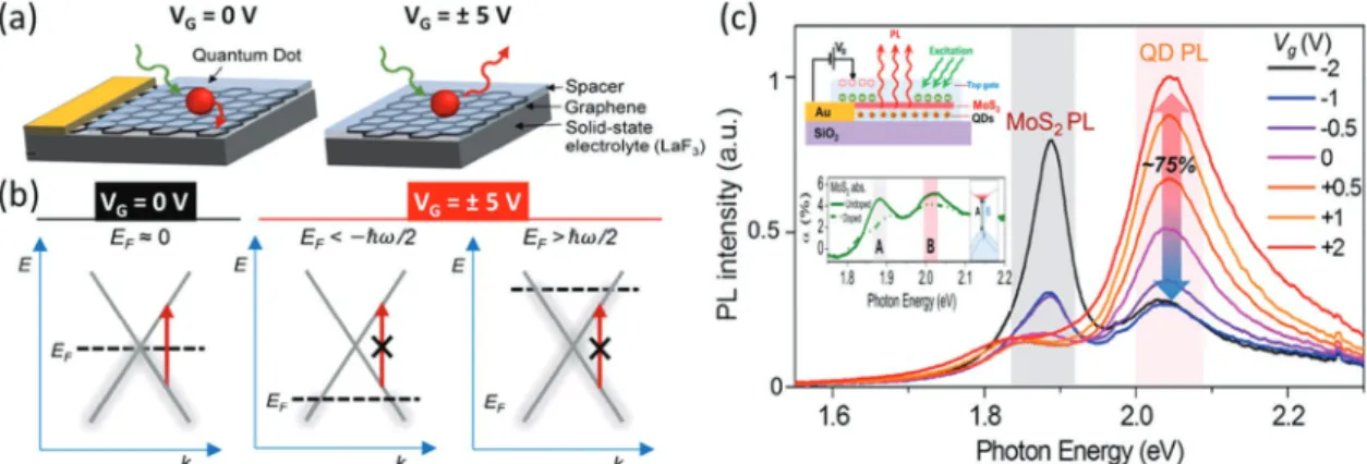
Another advantage of 2D materials is the ease of control-ling their photophysical properties through electrical means such as electrical gating.[108] Through electron filling of gra-phene, its Fermi level can be easily altered; therefore, interband transitions can be manipulated. In the last few years, several reports demonstrated that FRET from a nanoemitter into 2D materials could be turned on and off by electrical control on demand.[29,102,109] Ref. [102] demonstrated that through elec-trostatic doping, FRET from single quantum dots to graphene could be reversibly inhibited. This was possible thanks to the modulation of the Fermi level of graphene via electron filling. Figure 5a shows the proposed back-gated graphene–quantum dot hybrid device. When the gate voltage is zero, the Fermi level (EF≈0) is approximately at the crossing point between
conduction and valence bands. By applying gate voltage, it is possible to shift the Fermi level up (and down) by doping with electrons (holes). If 2 EF>hν E h F< − ν or 2, then interband
electronic transition at the photon energy (hv) will be disal-lowed (see Figure 5b). Therefore, this would block FRET from a nearby donor having a bandgap of hv. Ref. [102] employed
Figure 5. (a) Schematic of a back-gated graphene–quantum dot hybrid device. When VG = 0 V, FRET from quantum into graphene is allowed, thus
quantum dot emission is strongly quenched. When VG= ± 5 V, electrons (or holes) dope graphene such that interband transitions are blocked, thus
FRET is also blocked and quantum dot emission is recovered. (b) Energy band diagram demonstrating the modulation of the Fermi level of graphene via electronic gating. When VG = 0 V, EF ≈ 0 and interband transition at the photon energy of the donor (red arrow) is allowed. When VG = ± 5 V, then
2
EF>hν or
2
EF< −hν, interband transition at the photon energy of the donor is not allowed, thus, FRET is blocked. Panels (b) and (c) are reproduced
with permission.[102] Copyright 2014, American Chemical Society. (c) Steady state photoluminescence spectra of the monolayer MoS
2–quantum dot
hybrid device under different gate voltages. Quantum dot emission could be modulated by 75% due to modulation of FRET rate into MoS2. The top-left
inset shows the device structure. The bottom-left inset shows the modulation of the absorption (solid for VG = 0 V, dashed for VG ≠ 0 V) of single-layer
FEA
TURE AR
TICLE
PbS quantum dots having a bandgap in the range of 0.9–1.3 eV, where photo luminescence of the quantum dots could be mod-ulated with a ratio larger than 2.3 folds by the gate-induced doping of graphene. Based on a similar approach, Koppens et al. also demonstrated electrical control of near-field energy transfer from excited erbium ions (∼0.83 eV) to graphene by a rate modulation ratio of more than 3.[109]
In addition to graphene, the MoS2 monolayer was proposed for electrical control of the FRET.[29] MoS
2 exhibited suppressed absorption at its excitonic peaks under electrostatic gating. Therefore, the reduced absorption could be used to suppress the spectral overlap integral between the donor emission and the MoS2 absorption. In this work, a 5-fold modulation of FRET rate from CdSe/CdS quantum dots into MoS2 was realized. Figure 5c shows the steady-state photoluminescence spectra of the electrically gated MoS2–quantum dot hybrid device. Steady state photoluminescence emission of the quantum dots could be modified by 75%. One advantage of MoS2 compared to gra-phene is that FRET from the nanoemitters with a bandgap in the visible range could be controlled because the excitonic absorption of MoS2 is in the visible range. As compared to graphene-based devices, MoS2 devices could also operate at smaller applied voltages. Although the on/off contrast ratio of the current proof-of-concept devices are limited (up to 5-folds), the concept of active FRET control will be exciting to develop quantum emitters that can be turned on and off on demand.
Although exciton transferring nanoemitter–graphene hybrid systems are exciting for light harvesting, a significant limita-tion arises because transferred excitons into graphene cannot efficiently contribute to the photocurrent generation due to ultrafast thermalization of the hot electron (and hot hole) in graphene. Previously, energy transfer from nanoemitters into a metal surface was studied and the transferred electron–hole pairs were considered to be lost within the electron bath of the metal due to fast thermalization of the hot carriers.[110] Simi-larly, hot carrier relaxation in graphene typically takes place at ultrafast time scales (e.g., sub-picosecond),[111] thus, resonantly transferred excitation energy is most probably lost to heating before it could be contributed to the photocurrent. As a poten-tial solution to this problem in graphene, Ref. [112] recently reported an ultrafast photocurrent sensing scheme based on ultrafast photoconductive switches (e.g., Auston switches[113]). Closely separated striplines that act as an antenna on gra-phene were used for the ultrafast photoconductive detection and photocurrent extraction. Electron–hole pairs created in the graphene (either directly created or transferred via FRET) were swept out with the applied bias across two striplines. This generated an electromagnetic transient response in the strip-line, which is sensed by a pump–probe scheme. The meas-ured transient photocurrent revealed the contribution from the transferred electron–hole pairs from the nitrogen vacancy centers into the graphene. Resonantly transferred electron-hole pairs could be harvested and photocurrents on the order of pA level could be generated.
In addition, TMDC monolayers, which are semiconductors with a finite bandgap, are more suitable for harvesting the transferred excitons for photodetection because they have rel-atively long excited state lifetime. In TMDCs, the transferred electron and hole relax to the band edge and stay stable as the
exciton for few ns, allowing enough time for photocurrent extraction, yet strong exciton binding energies in TMDC mono-layers may cause difficulties for exciton dissociation. To this end, heterostructured TMDC layers having Type-II band align-ment are promising for enhanced photocurrent generation and photovoltaics.[114]
In contrast to exciton transfer, charge transfer into 2D materials also created exciting opportunities for photo-sensing devices.[92,115] Generally, core-only quantum dots have been employed, such as PbS quantum dots, because charge transfer is impeded in core/shell quantum dots. In addition to graphene, charge transfer has been observed from PbS quantum dots into reduced graphene oxide.[116] Furthermore, MoS2–PbS quantum dot hybrids also accomplished efficient photodetection performance.[115]
6. Efficient Exciton Transport Using
Colloidal Nanoplatelets
Recently, colloidal CdX (X = Se, S, and Te) nanoplatelets have emerged as an exceptional addition to the class of semicon-ductor nanocrystals. The colloidal nanoplatelets possess atomi-cally flat surfaces while their vertical thickness is only a discrete number of CdX monolayers. The lateral size of the nanoplate-lets is typically larger than the exciton Bohr radius. Therefore, effectively one-dimensional quantum confinement is observed, which makes them colloidal analogues of epitaxial quantum wells. The nanoplatelets have exhibited superior optical properties compared to those of conventional nanocrystals (e.g., quantum dots).[10,117] Due to very tight confinement in one dimension and strong dielectric screening, electron and hole are strongly bound with an exciton binding energy in excess of 200 meV.[118] This leads to very large oscillator strength[119] in the nanoplatelets, allowing them to bear large linear[71,120] and nonlinear[121,122] absorption cross-section together with fast radiative recombination rates.[10] Also, there is no inho-mogeneous size broadening in the nanoplatelet ensembles due to their atomically flat surfaces and fixed vertical thick-nesses, which are also denoted by discrete number (i.e., mon-olayers) of the repeating lattice planes.[123,124] Thanks to their advantageous properties, the nanoplatelets have become highly promising for optoelectronics with remarkable performance in solution-processed lasers,[125] light-emitting diodes,[126] and photodetectors.[127]
The potential for strong light-matter interactions in the nanoplatelets, similar to 2D semiconductors, make them exciting candidates for efficient exciton transfer at the nanoscale. In Ref. [31], we uncovered ultrafast exciton transfer among CdSe nanoplatelets in their face-to-face stacked assem-blies (see Figure 6), which form due to strong van der Waals forces.[128] We controllably stacked the nanoplatelets that were dissolved in hexane by slowly adding an anti-solvent (ethanol). As face-to-face stacking occurs, photoluminescence intensity was strongly quenched and simultaneously fluorescence decays became faster, suggesting an overall increase in the nonradia-tive recombination rate in the nanoplatelet ensembles.
We accounted for these observations by ultraefficient FRET-assisted exciton trapping in the nanoplatelets. We estimated a
FEA
TURE AR
TICLE
very large Förster radius of 13.5 nm (see Table 1) for the homo-FRET between nanoplatelets having the same vertical thick-ness (four monolayer CdSe). This large Förster radius was enabled by the large linear absorption cross-section and very small Stokes shift in the nanoplatelets together with collinear orientation of the transition dipoles in their face-to-face stacked assemblies. The Förster radius for the nanoplatelet acceptors is almost two folds larger than that of the conventional quantum dot acceptors (see Table 1). Also, it is comparable to the largest reported Förster radius using 2D materials such as graphene and TMDC monolayers.
In the face-to-face assembled nanoplatelets, we predicted FRET efficiency as high as 99.9% with an ultrafast FRET lifetime of 3 ps for the two neighboring nanoplatelets in the stacked assembly, which offers minimized separation distance (≈4.2 nm) between the nanoplatelets. Previously, the fastest FRET lifetime among colloidal nanocrystals was reported ≈100 ps.[72,129] Thus, colloidal nanoplatelets stand out as ultra-fast exciton scavengers among colloidal semiconductors. More-over, we estimated an effective exciton diffusion length that is larger than 130 nm.[31] The exciton diffusion would be also directed and anisotropic due to the needle-like geometry of the stacked assemblies (see Figure 6). Previously, exciton diffu-sion in the colloidal quantum dots was found to be limited by ∼20 nm due to sub-diffusive exciton transport[73] arising from downhill transport in the inhomogeneously broadened density of states due to size polydispersity in the quantum dots. This had caused a strong red-shift of the emission due to homo-FRET
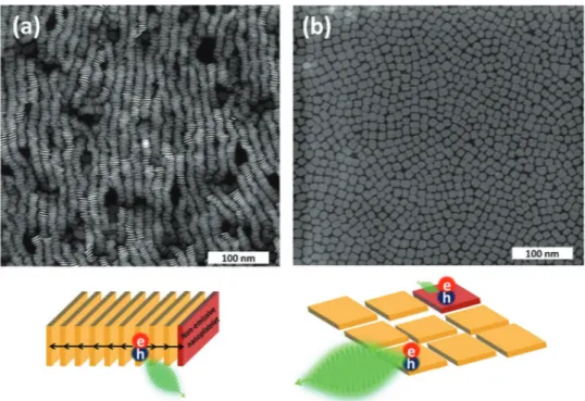
in close-packed quantum dot films.[130] In contrast, we did not observe a red-shift of the nanoplatelet emission because inho-mogeneous broadening is substantially suppressed. Previously, perovskite films showed comparable exciton diffusion lengths in excess of 100 nm.[131] Further studies based on nanoscale exciton diffusion visualization will be extremely useful in the nanoplatelet assemblies.[132,133] Achievement of ordered, needle-like, stacked nanoplatelet films[134] will be promising for the solution-processed solar cells, photodetectors, and artificial photosynthesis thanks to the potential of ultralong exciton dif-fusion length. In Figure 6, we show our results on achieving ordered needle-like nanoplatelet films on TEM grids via an air/ liquid self-assembly technique.[135] Highly ordered nanoplatelet stacks with more than 100 nanoplatelets per stack could be achieved at relatively large areas.
On the other hand, we found that nanoplatelet ensembles contain a sub-population of poorly-emitting nanoplatelets due to the presence of surface traps in some of the nanoplate-lets,[121] which was also observed and reported by others.[136,137] Theoretical modeling strongly suggested that ultraefficient FRET-assisted exciton trapping is the dominant mechanism of the photoluminescence quenching in face-to-face assem-bled nanoplatelets. Ultraefficient exciton transport among the nanoplatelets within the stack leads to an increased capturing rate for the non-emissive nanoplatelets. Figure 7 shows both face-to-face and side-by-side assembled nanoplatelets. In the face-to-face stacked assembly, ultraefficient exciton transfer among the nanoplatelets leads to increased exciton trapping Figure 6. High-angle annular dark-field transmission electron microscopy (HAADF-STEM) image of highly ordered face-to-face stacked CdSe nanoplatelets
with scale bars (a) 500 nm and (b) 200 nm. The region in (b) is from the dashed area in (a). Highly ordered needle-like nanoplatelet stacks were achieved as shown by the representative schematic in (c). In the absence of non-emissive nanoplatelets, ultralong exciton diffusion length (>100 nm) is expected.
FEA
TURE AR
TICLE
in the poorly emissive nanoplatelets. When exciton ends up in a poorly emissive nanoplatelet, exciton is nonradiatively quenched by either hole or electron trapping (see Figure 7a). In mosaic-like side-by-side assembled nanoplatelets, exciton transfer is not dominant because the donor–acceptor distance is large. Therefore, this assembly is more favorable to preserve the photoluminescence intensity in the presence of non-emis-sive nanoplatelets (see Figure 7b).
FRET-assisted exciton trapping in the face-to-face stacked nanoplatelets was also evidenced by studying temperature-dependent photoluminescence kinetics in face-to-face stacked nanoplatelets.[138] In this recent work, we found that sparsely side-by-side stacked nanoplatelets exhibit considerably increased photoluminescence intensity as the temperature is decreased. This was previously attributed to the increased oscil-lator strength in the nanoplatelets at low temperatures, which increases their emission quantum yield.[10] On the other hand, face-to-face stacked nanoplatelets showed 5-folds less increase as the temperature was decreased in the same range. Through the-oretical modeling, we revealed that FRET-assisted exciton trap-ping becomes more efficient as oscillator strength is increased at low temperatures. Therefore, exciton trapping grows stronger at low temperatures in the face-to-face stacked nanoplatelets.
In addition to homo-FRET, hetero-FRET was also investi-gated among nanoplatelet ensembles. First, we demonstrated that FRET is possible from four monolayer- into five mon-olayer-thick CdSe nanoplatelets.[33] In this work, we showed unambiguous evidence of FRET via time-resolved fluores-cence and photoluminesfluores-cence excitation spectra. Although we estimated a Förster radius of ca. 11 nm (see Table 1), we unexpectedly found that FRET efficiencies are limited by 60%
(see Figure 8a). Through electron microscopy, we discovered that four- and five-monolayer CdSe nanoplatelet stack in their own populations due to their different lateral sizes (see the schematic in Figure 8a). Consequently, the effective distance between the donor and the acceptor is large, considerably lim-iting FRET. Thus, we could not achieve ultrafast FRET due to nanoscale morphology of the nanoplatelets. On the other hand, Talapin et al. were able to interstack four- and five-monolayer-thick CdSe nanoplatelets together (see inset of Figure 8b).[139] Thus, ultrafast FRET rates were measured using streak camera, exhibiting FRET rates as fast as 6 ps (see Figure 8b). This report is in excellent agreement with our prediction of 3 ps FRET rate in Ref. [31]. Moreover, the ultrafast FRET rates observed by Refs. [139] and [31] suggest that self-assembled nanoplate-lets will be highly suitable for realizing efficient FRET in the multiexciton regime, which has not been possible before using conventional quantum dots. This will make the nanoplatelets exciting prospects for solar light harvesting.
In addition to nanoplatelet–nanoplatelet systems, we recently employed nanoplatelets as exciton harvesters from blue-emit-ting CdZnS/ZnS core/shell quantum dots.[32] By assuming random dipole orientation due to isotropic donor quantum dots, we calculated an ≈9 nm Förster radius (see Table 1). Quantum dots and nanoplatelets mixed well together without phase segregation, allowing us to achieve FRET efficiencies as high as 90% at room temperature (see Figure 9a). an interesting feature of these hybrids was that they exhibited an exceptionally linear response for the FRET efficiencies as a function of tem-perature in the range of 300–50 K (Figure 9b). The dominant effect behind this linear FRET behavior was found to be the temperature-dependent PL QY of the donor quantum dots.[32] Figure 7. HAADF-STEM images of (a) face-to-face and (b) side-by-side stacked nanoplatelet assemblies realized by air/liquid self-assembly technique.
(a) FRET-assisted exciton trapping by non-emissive nanoplatelet leads to strongly quenched emission. (b) Exciton trapping is suppressed as dipole-dipole coupling is weaker due to increased separation distance between the nanoplatelets in the side-by-side stacked assemblies.
FEA
TURE AR
TICLE
Also, the change of the temperature-dependent spectral overlap played a minor role in the observed FRET efficiencies. There-fore, this hybrid system could be employed as non-contact temperature probes. The sensitivity of the quantum dot–nano-platelet hybrid was found to be 3.2% K–1, which is comparable to the best report (3.5% K–1[140]) using a ratio metric sensing scheme. Here, our hybrid systems employed FRET efficiencies for temperature sensing, which can be characterized via time-resolved fluorescence techniques, thus allowing for increased robustness and reliability compared to ratio metric sensing that depend on emission intensities.
7. Dexter Energy Transfer for Triplet-State
Exciton Harvesting
In the last decade, organic semiconductor–colloidal nanocrystal hybrids have been explored owing to their promising application
in solar cells[141] and light-emitting diodes.[142,143] A commonly studied excitonic process in the organic-nanocrystal hybrids is the spin-singlet exciton transfer.[144–147] Exploiting organic– nanocrystal hybrids that exhibit highly efficient exciton transfer, we developed hybrid LEDs, in which quantum dot emitters were dominantly pumped by exciton transfer by the organic semi-conductor.[36] Although these excitonically pumped hybrid LEDs make interesting alternatives to charge injection pumping, they are limited by the use of fluorescent organic semiconductors. Under free carrier injection, ¾ of the formed excitons in a fluo-rescent organic molecule are in spin-triplet state. Thus, it was not possible to harvest these triplet excitons via FRET because triplet states have almost zero oscillator strength.
Triplet-state exciton harvesting in organic–nanocrystal hybrids were addressed by employing phosphorescent small organic molecules, which have mixed singlet-triplet states due to strong intersystem crossing. As a result, FRET became fea-sible when using phosphorescent molecules as exciton donors, Figure 8. (a) FRET efficiency as a function of acceptor (five-monolayer) to donor (four-monolayer-thick CdSe nanoplatelet) molar ratio. FRET
efficien-cies were unexpectedly saturated around 60% due to nanoscale phase segregation arising from the self-stacking of the donor and acceptor on their own as shown by the cartoon at the bottom. Reproduced with permission.[33] Copyright 2015, Royal Society of Chemistry. (b) Experimental evidence of
ultra-fast FRET rate (≈6 ps) from four- to five-monolayer-thick CdSe nanoplatelets that are interstacked together as shown by the cartoon on top-right. Reproduced with permission.[139] Copyright 2015, Nature Publishing Group.
Figure 9. (a) FRET efficiency in colloidal quantum dot–nanoplatelet nanocomposites as a function of donor (quantum dot) to acceptor (nanoplatelet)
molar ratio. (b) Temperature-dependent FRET efficiency in quantum dot–nanoplatelet nanocomposite. Panels (a) and (b) reproduced with permission.[32]
FEA
TURE AR
TICLE
which was revealed by time-resolved fluorescence and photo-luminescence excitation measurements.[38,148] Although FRET rates were slow (k 1 50ns
FRET− ≈ ) in these hybrids, overall FRET
efficiencies were found to be as high as 90%[38] due to an intrin-sically slow radiative decay rate in the phosphorescent mol-ecules. Also, relatively large Förster radius (6 nm, see Table 1) was predicted for the cyan-emitting FIrpic phosphorescent donor–red-emitting CdSe/CdZnS core/shell quantum dots (see Table 1). We also deployed phosphorescent molecule–quantum dot hybrids in active LEDs to harvest both singlet and triplet excitons. Ir(ppy)3 molecules were partially co-doped into an electron transport layer adjacent to the emissive quantum dot layer.[149] Excitons formed in the co-doped layer due to leaking holes through the quantum dot film were recycled back into the emissive layer via FRET. This exciton recycling within hybrid LEDs resulted in a 6-fold increase in the external quantum efficiency of the devices while preserving an excellent spectral color purity (99% from the quantum dots).[149]
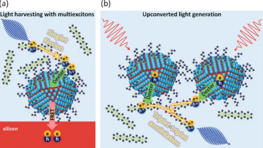
More recently, spin-triplet excitons in small organic mole-cules (e.g., pentacene and tetracene) were shown to be efficiently transferred into colloidal quantum dots (e.g., PbS and PbSe) via Dexter energy transfer.[150–152] This nonradiative energy transfer was shown to achieve ultrafast transfer rates (≈few ps)[151] with transfer efficiencies reaching almost unity.[152] These studies fur-ther highlighted that colloidal quantum dots make highly effi-cient sensitizers to exploit ultraeffieffi-cient multiexciton processes in organic semiconductors such as singlet exciton fission[153,154] (S1→2T1) and triplet-triplet annihilation[155] (2T1→S1). Thus,
organic–nanocrystal hybrids are expected to pave the way for efficient-use molecular excitons to harness light more efficiently in solar cells or enhance light generation performance in hybrid LEDs and upconversion systems.
Figure 10 schematically exemplifies two schemes that deploy organic–nanocrystal hybrids for efficient light-harvesting and upconversion applications. In Figure 10a, a high energy photon absorption generates singlet exciton in the organic semicon-ductor. Through singlet exciton fission, two triplet excitons can be formed from a singlet exciton with exceptionally high effi-ciencies (≈200%).[154] These triplet excitons can then be trans-ferred to colloidal quantum dots via Dexter energy transfer. Afterwards, the quantum dots can either emit a longer wave-length photon or can transfer the excitation energy into another semiconductor (e.g., silicon) via nonradiative energy transfer, as previously discussed. With this scheme, light harvesting with internal quantum efficiencies exceeding 100% can be achieved owing to the exploitation of the multiexciton generation.[156]
Figure 10b schematically illustrates a hybrid upconversion scheme that employs NIR–IR-absorbing quantum dots and vis-ible-emitting organic molecules. Colloidal quantum dots, which have a smaller bandgap than the first singlet exciton energy of the organic molecule, can transfer its exciton into the organic molecule via Dexter energy transfer. As a consequence, triplet excitons are generated in the organic molecule, which can form higher-energy singlet excitons via triplet-triplet annihilation (i.e., triplet fusion). Singlet excitons in the organic molecule will emit visible photons. Thus, efficient IR-to-visible upconver-sion can be achieved by using quantum dots having a tunable bandgap in IR region.
Organic semiconductor–colloidal nanocrystal hybrids that perform upconversion were recently realized using small-bandgap Cd- and Pb-chalcogenide quantum dots by transferring their excitons into the triplet states of larger-bandgap organic molecules (e.g., diphenylanthracene, rubrene and 9-anthra-cenecarboxylic acid, naphthyl).[157–160] Previously, IR-to-visible
Figure 10. (a) A sensitization scheme for silicon solar cells based on organic semiconductor–colloidal nanocystal hybrids. A singlet exciton generated
by absorption of high energy photons leads to the generation of two triplet state excitons via singlet exciton fission. Triplet excitons are harvested by the quantum dots through Dexter energy transfer. Excitons in the quantum dots can be transferred into silicon via FRET or RET, increasing the overall power conversion efficiencies. (b) An upconversion scheme based on organic semiconductor–colloidal nanocrystal hybrids. Excitons generated by IR photons in the quantum dots are resonantly transferred into molecules as triplet excitons via Dexter energy transfer. Stored triplet excitons can perform triplet-triplet annihilation to form high energy singlet excitons that emit photons in the visible range.