T.C.
ISTANBUL AYDIN UNIVERSITY
INSTITUTE OF NATURAL AND APPLIED SCIENCES
NEW MICRO-INVERTER FOR PHOTOVOLTAIC APPLICATIONS
THESIS
Murtala Abdulmumini Rafindadi
Department of Electrical & Electronic Engineering Electrical and Electronics Engineering Program
T.C.
ISTANBUL AYDIN UNIVERSITY
INSTITUTE OF NATURAL AND APPLIED SCIENCES
NEW MICRO-INVERTER FOR PHOTOVOLTAIC APPLICATIONS
THESIS
Murtala Abdulmumini Rafindadi (Y1713.300028)
Department of Electrical & Electronic Engineering Electrical and Electronics Engineering Program
Advisor: Prof. Dr Murtaza FARSADI
v
DECLARATION
I hereby declare that all information in this thesis document has been obtained and presented in accordance with academic rules and ethical conduct. I also declare that, as required by these rules and conduct, I have fully cited and referenced all material and results, which are not original to this thesis.
vii FOREWORD
I would first like to thank my family, my father,Prof Abdulmumini Hassan Rafindadi and mother Haj. Hassana Abdulmumini Rafindadi who have always been supportive and encouraging, they raised me to become a good person and a positive member of society and were patient with me through good and better days and everthing i have accomplished is because of their effort and i hope i can make them happy in return for all they have done for me and also my brother Mustapha and sister Zainab for all the support and encouragment. I would like to thank my thesis advisor Prof. Dr. Murtaza Frasadi of Electric and Electronic Engineering department at Istanbul Aydin University. The door to Prof. Murtaza Frasadi’s office was always open whenever I ran into a trouble spot or had a question. He consistently allowed this paper to be my own work but steered me in the right the direction whenever he thought I needed it.
I would like to thank all my teachers for having great influence on me, I would like also to thank department of Electric and Electronic Engineering and also Istanbul Aydin University and its library for providing me with access to all the books and articles that I needed to finish this work
October, 2019 Murtala Abdulmumini Rafindadi
ix TABLE OF CONTENT Page FOREWORD ... vii TABLE OF CONTENT ... ix ABBREVIATIONS ... xi
LIST OF FIGURES ... xiii
LIST OF TABLES ... xv
ABSTRACT ... xvii
ÖZET ... xix
1. INTRODUCTION ... 1
1.1 Purpose ... 1
1.2 Solar Power Systems ... 1
1.2.1 First Generation ... 2
1.2.2 Second Generation ... 2
1.2.3 Third Generation ... 2
1.3 PV Power Generation System ... 2
1.4 Thesis objective ... 3
1.5 Thesis outline ... 4
2. THEORY OF THE INVERTERS ... 5
2.1 What is an inverter? ... 5
2.2 How does an inverter works? ... 5
2.3 Different Types of inverters in pv systems ... 6
3. PV SYSTEMS ... 9
3.1 History of Pv frameworks ... 9
3.2 How PV Cells Work. ... 9
3.3 Cells, Modules, and Arrays. ... 10
3.4 How a PV System Works? ... 12
3.5 For what reason Are Batteries Used in Some PV Systems? ... 13
3.6 Types of PV Systems. ... 13
3.6.1 Stand-alone Photovoltaic Systems ... 14
4. PROPOSED NEW HYBRID BF/F MICRO INVERTER ... 17
4.1 Flyback inverter operated in different conduction modes ... 17
4.2 Operating Technique ... 18
4.3 Operating Principle ... 20
4.4 Proposed Reference Current ... 25
5. DESIGN CONSIDERATION AND CHARACTERISTIC ANALYSIS ... 29
5.1 The below figure is the main circuit which shows the micro-inverter ... 29
5.1.1 Solar Panel Design ... 29
5.1.2 Hybrid BF/F Converter ... 30
5.1.3 Unfolding stage ... 31
5.1.4 Grid ... 31
5.1.5 Control panel ... 32
x
5.2.1 Coupled Transformer ... 38
6. SIMULATION RESULTS. ... 47
6.1 Comparism between inverters ... 52
7. CONCLUSION ... 57
7.1 Conclusion ... 57
7.2 Future works ... 57
REFERENCES ... 59
xi ABBREVIATIONS
BCM : Boundary Condition Mode
BF : Boost Flyback
CCM : Continuous Conduction Mode
DCM : Discontinuous Conduction Mode
DILC : Down sampled Iterative Learning Controller DPSM : Distributed Power-Generation System EMI : Electromagnetic Interference
F : Flyback PI : Proportional Integral PR : Proportional Controller Pv : Photovoltaic QR: : Quasi-Resonance RC : Repetitive Controller RHP : Right-Half-Phase
THD : Total Harmonic Distortion
VS : Valley Switching
ZCS : Zero-Switching
xiii LIST OF FIGURES
Page Figure 1.1: Market share of cumulative installed PV capacity, by application (IEA
2011) ... 3
Figure 2.1: diagram of basic Inverter ... 6
Figure 3.1: Diagram of a photovoltaic cell ... 10
Figure 3.2: Photovoltaic cells, module, panels and arrays ... 11
Figure 3.3: Major Pv system componenets ... 12
Figure 3.4: Diagram of grid-connected photovoltaic system ... 14
Figure 3.5: Direct-coupled PV system ... 15
Figure 3.6: Diagram of stand-alone PV system with battery storage powering DC and AC loads ... 15
Figure 3.7: Diagram of photovoltaic hybrid system. ... 16
Figure 4.1: Proposed New Hybrid Bf/F Micro Inverter ... 17
Figure 4.2: Key waveforms of the new micro-inverter in BCM ... 20
Figure 4.3: Operating waveforms under BF mode ... 21
Figure 4.4.1: Mode I (T0-T1) ... 22
Figure 4.4.2: Mode II (T1-T2) ... 23
Figure 4.4.3: Mode III (T2-T3) ... 24
Figure 4.4.4: Mode IV (t3-t4) ... 24
Figure 4.4.5: Mode V(t4-t5) ... 25
Figure 4.5: Waveforms of primary and output current under BF mode ... 27
Figure 5.1: Proposed new micro-inverter ... 29
Figure 5.2: Solar panel module ... 29
Figure 5.3: BF/F converter ... 30
Figure 5.4: Unfolding stage of the converter ... 31
Figure 5.5: The grid with load ... 32
Figure 5.6: Structure of MPPT ... 33
Figure 5.7: Structure of PLL ... 33
Figure 5.8: the internal diagram of PLL ... 34
Figure 5.9: The PID system block ... 35
Figure 5.10: internal circuit of PID controller in the controller ... 36
Figure 5.11: shows the waveform of how PWM occurs ... 37
Figure 5.12: shows the control circuit which contains the MPPT and unfolding controllers ... 38
Figure 5.13: Discharging conduction path for output capacitor C2 ... 40
Figure 5.14.1: Reference current ... 42
Figure 5.14.2: Drain-to-source voltage ... 43
Figure 6.1: shows current and power for the Pv panel module ... 48
Figure 6.2: Wave forms of Vo ... 49
Figure 6.3: Grid Voltage (Vg) ... 49
xiv
Figure 6.5: The switches Q1at line frequency and at double line frequency (120Hz)
Q,2Q3, ... 50
Figure 6.6.1: Waveforms of Id1 ... 51
Figure 6.6.2: Waveforms Id2 ... 51
Figure 6.6.3: Waveforms Vds ... 51
Figure 6.7: Grid output voltage and current waveforms ... 52
Figure 6. 8: Single-Stage Grid-Connected Flyback Micro-inverter ... 52
Figure 6. 9: Output voltage of result of Single-Stage Grid-Connected Flyback Microi-nverter ... 53
Figure 6.10: Circuit diagram of Photovoltaic flyback micro-inverter with power decoupling technique ... 53
Figure 6.11: Output waveforms of Photovoltaic flyback micro-inverter with power decoupling technique ... 54
Figure 6.12: Show the circuit diagram of Single Phase PV based Micro Inverter with an Optimal Controller ... 54
Figure 6.13: Show the output waveforms of Single Phase PV based Micro Inverter with an Optimal Controller ... 55
xv LIST OF TABLES
Page
Table 5.1: Parameters of solar panel module ... 30
Table 5.2: Parameters of load ... 31
Table 5.2: Mathematical expressions of PID ... 36
Table 6.1: Circuit Parameters ... 47
xvii
NEW MICRO-INVERTER FOR PHOTOVOLTAIC APPLICATIONS ABSTRACT
Solar systems work by using special solar cells that absorb solar energy. These cells are interconnected on a panel or array of various sizes depending on the particular energy demand. No matter how large or small a solar panel may be, it is connected to what is known as an inverter, which is designed to take the direct current (DC) power gathered and generated by the PV cells and convert that power into an alternating current (AC) which is compatible with the existing electrical grid that powers your home or commercial property. The AC output from the solar PV system is sent to your electrical panel where it is distributed accordingly for convenient use.
In photovoltaic applications, the micro inverter is well known for having large transformer turn ratio that results in large leakage inductance which will reduce the converters efficiency. The solution to the problem is the proposed new micro-inverter in this paper. This new micro-inverter operates based on boost-flyback/flyback(BF/F) modes, the BF mode is for the half grid cycle and the F is for the remaining parts. In BF operation mode, high voltage gain and low voltage stress is available in minimum transformer turn ratio. The leakage energy is then recovered and the turn-off voltage rise of the main switch is cut, as a result of a passive snub in the mode. The BF mode lacks a step-down function, the F mode is used to control the output voltage for values lower than the input voltage. The operation and characteristics of the micro-inverter in boundary condition mode are analysed in detail. A 240W prototype is enforced to validate the theory.
Keywords: Boost-flyback, minimized turn ratio, high voltage gain, low voltage stress, snub.
xix
FOTOVOLTAIK UYGULAMALAR IÇIN YENİ MİKRO İNVERTÖR ÖZET
Güneş sistemleri, güneş enerjisini emen özel güneş pilleri kullanarak çalışır. Bu hücreler, belirli bir enerji talebine bağlı olarak bir panel veya çeşitli boyutlarda bir dizi üzerinde birbirine bağlanır. Bir güneş paneli ne kadar büyük veya küçük olursa olsun, PV hücreleri tarafından toplanan ve üretilen doğru akım (DC) gücünü almak ve bu gücü alternatif bir akıma dönüştürmek için tasarlanmış bir invertör olarak bilinen şeye bağlanır. (AC) ev veya ticari mülkünüze güç sağlayan mevcut elektrik şebekesiyle uyumludur. Solar PV sisteminden gelen AC çıkışı, hızlı ve rahat kullanım için uygun şekilde dağıtıldığı elektrik panelinize gönderilir.
Fotovoltaik uygulamalarda, mikro invertörün, dönüştürücülerin verimliliğini düşürecek büyük kaçak endüktansı ile sonuçlanan büyük transformatör dönüş oranına sahip olduğu iyi bilinmektedir. Sorunun çözümü, bu yazıda önerilen yeni mikro invertördür. Bu yeni invertör, geri besleme / geri dönüş / geri dönüş (BF / F) modlarına göre çalışır, BF modu yarım ızgara döngüsü içindir ve F kalan parçalar içindir. BF çalışma modunda, minimum transformatör dönüş oranında yüksek voltaj kazancı ve düşük voltaj stresi mevcuttur. Sızıntı enerjisi daha sonra geri kazanılır ve moddaki pasif bir tıkanmanın bir sonucu olarak ana şalterin kapanma gerilimindeki artış kesilir. BF modu, bir kademeli fonksiyondan yoksundur, F modu, giriş voltajından düşük değerler için çıkış voltajını kontrol etmek için kullanılır. Mikro invertörün sınır koşulu modunda çalışması ve özellikleri detaylı olarak analiz edilir. 240W prototip, teoriyi doğrulamak için uygulanır.
Anahtar Kelimeler: Arttır-geri dönüş, minimize edilmiş dönüş oranı, yüksek voltaj kazancı, düşük voltaj gerilimi, snub.
1 1. INTRODUCTION
Abundant energy is the life blood of present day human advancement. With the expanding rate of worldwide financial development just as the noteworthy improvement in world industry, the quick rising interest for practical energy has put consistently expanding weight on human culture. In addition to the fact that humankind is coming up short on effectively realistic non-renewable energy source assets, however the related ecological effect of non-renewable energy source use is arriving at emergency levels. For this situation, environmentally friendly power energy, additionally named sustainable power source, is the best decision as an elective asset for the world business. For the most part, the standard advancements applied in the efficient power vitality field can be delegated wind power, hydro-control, solar power, geothermal power and biomass control. Alongside the astonishing developments in the photovoltaic (PV) innovation [11], sun based power has pulled in a lot of consideration. Because of a few reasons including the boundless vitality from the sun, the generally high effectiveness of current PV framework, the constantly dropping cost of sun based cells and the simplicity of execution and support of heavenly bodies, the PV industry is takin a big role in world energy supply supply [1].
1.1 Purpose
The purpose of this thesis is to reduce the large turn ratio of transformers in converters which improves the converters efficiency, this is done by operating the proposed new hybrid converter in BF/F mode, BF mode is the operating mode while the F mode is for resting. This topology enables high voltage gain and low voltage stress easily available with minimized transformer turn ratio.
1.2 Solar Power Systems
Solar systems work by utilizing special solar sun based cells that absorb sun energy. These cells are interconnected on a board of different sizes relying upon
2
a specific energy demand. Regardless of how enormous or little a sun oriented panel might be, it is connected with what is known as an inverter, which is intended to take the direct current (DC) control accumulated and created by the PV cells and convert that power into an alternating current (AC) which is compatible with the current electrical framework that powers your home or business property [11]. The AC output from the sun solar PV framework is sent to your electrical panel where it is distributed according to convenient use. 1.2.1 First Generation
The first generation uses wafer-based crystalline silicon (c-Si) innovation, either single crystalline (sc-Si) or multi-crystalline (mc-Si). Single-crystalline cells are more proficient than multi-crystalline cells yet are increasingly costly to fabricate. This age is commanded by Silicon (Si) and some degree Gallium-Arsenide (GaAs) and is one of the standard PV innovations utilized today. 1.2.2 Second Generation
The subsequent age depends on thin-film PV innovations and can be grouped into three sorts: 1) amorphous (a-Si) and micromorph silicon (a-Si/uc-Si); 2) Cadmium-Telluride (CdTe); and 3) Indium-Selenide (CIS) and Copper-Indium-Gallium-Diselenide (CIGS). Other PV cell innovations incorporate the multi-intersection PV cells which ingest and convert more sunlight based range into power contrasted and single-intersection cells. The thin-film PV cells are the 4 generally utilized in the present market.
1.2.3 Third Generation
The third generation PV cells incorporate advances, for example, concentrating PV (CPV), dye sensitized, organic PV cells and quantum dots, which are still a work in progress and could be become viable commercial option in the future to diminish the expense
1.3 PV Power Generation System
The PV Generation can be commonly divided into two parts: off-grid systems and grid-connected system. The off-grid frameworks produce power Independently of the utility grid. Examples are telecommunications Units,
3
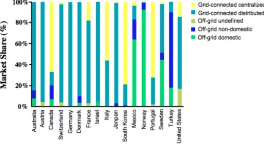
remote stations, rural power supply, and auxiliary power units for emergency or military applications. Up until the mid-1990s, most PV frameworks were standalone off-grid applications. The Grid-connected frameworks are connected with the Utility Grid. A portion of these frameworks feed the nearby load necessity first and give surplus power into Grid, while others feed all the Power into the Grid without considering about local load. Since the utility network gives boundless storage control, the system could deal with enormous load varieties [12].
Since 2005, the grid systems have relentlessly gained market because of government' advancements. Today they represent about 75% of the worldwide PV market today.
Figure 1.1: Market share of cumulative installed PV capacity, by application (IEA 2011)
1.4 Thesis objective
To propose a new hybrid micro-inverter that has high step-up ratio, minimized turn ratio, minimized voltage stress, minimized leakage inductance and inherent passive snubber as well as step down function to solve the issue of boost-flyback converter not regulating the output voltages for values lower than the input voltage.
4 1.5 Thesis outline
A new hybrid micro-inverter with the combination of boost-flyback and flyback converter, in which a pair of switches, worked complementarity at double-fine frequency, is incorporated into the boost-flyback converter for the operation mode change between BF and F mode. This new topology acquires the benefits of boost-flyback converter, for example, high step-up ratio, limited turn ratio, limited leakage inductance, limited voltage stress and intrinsic detached snubber, just as the step-down function of flyback converter, in this manner tackling the issue that the boost-flyback converter can't control the output voltage for values lower than the input voltage. The BCM operation with peak current control is received to achieve higher power density and transformation efficiency. A mathematical articulation for reference current is proposed through hypothetical deduction for higher power quality, Furthermore the characteristic of this topology is analyzed in detail.
5 2. THEORY OF THE INVERTERS
2.1 What is an inverter?
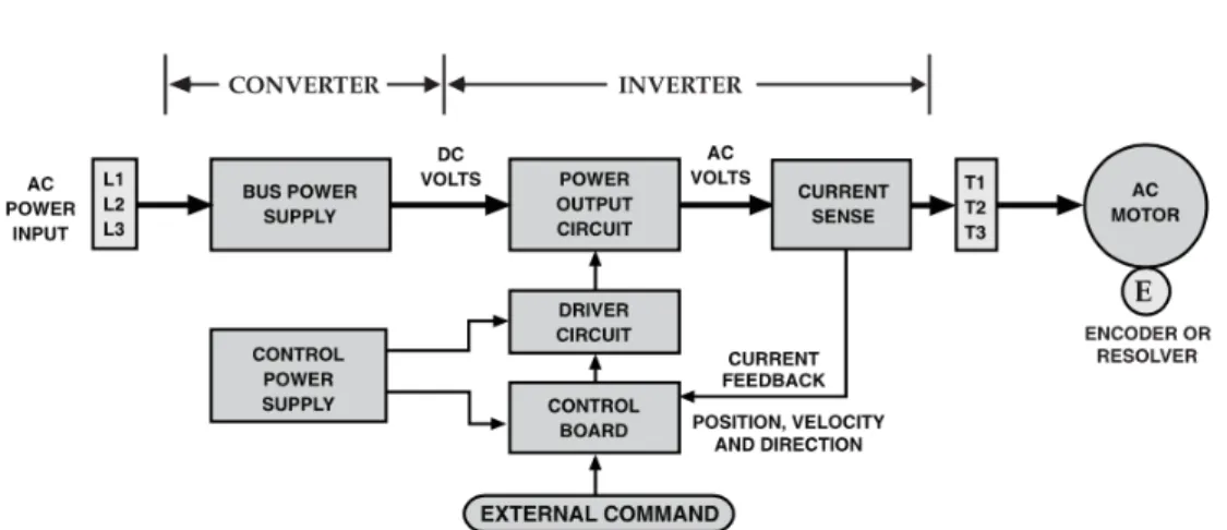
An inverter is a motor control that changes the speed of an AC inductor motor. It does this by changing the frequency of the AC capacity to the motor. An inverter additionally changes the voltage to the motor.
This procedure happens by utilizing some complicated electronic hardware that controls six separate power gadgets. They switch on and off to create a simulate three stage AC voltage. This exchanging procedure is additionally called inverting DC bus voltage and current into the AC waveforms that are applied to the motor. This prompted the name "inverter".
2.2 How does an inverter works?
Most inverters are of the variable voltage, variable frequency structure. They comprise of a converter segment, a bus capacitor area and an altering segment. The converter segment utilizes semiconductor gadgets to amend (convert) the approaching fixed voltage, fixed recurrence 3-phase AC capacity to DC voltage which is put away in the transport capacitor bank. There it turns into an unfaltering wellspring of current for the power gadgets which are situated in what is known as the inverting segment [2]. The transforming segment retains control from the DC bus bank, rearranges it back to recreated 3-Phase AC sine waves of shifting voltage and differing frequency that are commonly used to change the speed of a 3-stage inductor motor.
6
Figure 2.1: Diagram of basic Inverter 2.3 Different Types of inverters in pv systems
A. String Inverters
These are the most widely recognized sort of inverter utilized for private purposes. All the solar powered inverters are essentially a string inverters. It is known as a string inverter because they have large number of strings are associated on them.
B. Central Inverters solar-inverters
There are an enormous variety of inverters that are utilized for the solar systems in the couple of megawatts to the several kilowatts. Central Inverters look like enormous metal cupboards. It can deal with up to 500kW per fenced in area. They are not appropriate for homes and for the most part utilized for utility-scale solar based farms or enormous business establishments.
C. Micro inverters
Smaller scale inverters are essentially minor solar powered inverters about the size of the soft cover book. There are different focal points of micro inverters where they enhance each solar panel independently. It conveys more energy if you have partial shade conditions. In this, the emphasis is just a single inverter that you keep first on the list.
7 D. Hybrid Inverters
It is otherwise called multi-mode inverters. It enables you to connect batteries to your solar powered framework. This inverter interfaces the battery by utilizing a system called 'DC coupling'. Electronics organize the releasing and charging of the battery. There is a genuinely restricted decision on the hybrid inverters.
E. Battery Inverters
if you want to retrofit batteries to your solar power framework or basically keep your battery system separate from your solar panels. At that point for this, isolated battery inverter is the best decision. It just changes over your battery control into the 230V AC. At that point it feeds it into your switchboard where grid power is required.
9 3. PV SYSTEMS
3.1 History of Pv frameworks
The primary traditional photovoltaic cells were delivered in the late 1950s, and all through the 1960s were basically used to give electrical capacity to earth-circling satellites. During the 1970s, enhancements in assembling, execution and nature of PV modules diminished expenses and opened up various open doors for controlling remote terrestrial applications, including battery charging for navigational guides, signals, media communications gear and other basic, low-control needs [3].
During the 1980s, photovoltaics turned into a famous power hotspot for consumer electronic gadgets, including mini-computers, watches, radios, lights and other little battery-charging applications. Following the vitality emergencies of the 1970s, huge endeavours likewise started to create PV control frameworks for private and business utilizes, both for remain solitary, remote power just as for utility-associated applications. During a similar period, universal applications for PV frameworks to control rustic wellbeing centres, refrigeration, water siphoning, media communications, and off-network family units expanded significantly, and stay a significant segment of the present world market for PV items. Today, the industry's creation of PV modules is developing at roughly 25 percent every year, and significant projects in the U.S., Japan and Europe are quickly quickening the execution of PV frameworks on structures and interconnection to utility systems.
3.2 How PV Cells Work.
A basic silicon PV cell is made out of a dainty wafer comprising of an ultra-slight layer of phosphorus-doped (N-type) silicon over a thicker layer of boron-doped (P-type) silicon. An electrical field is made close to the top surface of the cell where these two materials are in contact, called the P-N intersection. At the point when sunlight strikes the outside of a PV cell, this electrical field gives
10
energy and course to light-animated electrons, bringing about a progression of flow when the solar cell is associated with an electrical load
Figure 3.1: Diagram of a photovoltaic cell
Regardless of the size, a basic silicon PV cell delivers about 0.5 – 0.6 volt DC under open-circuit, no-load conditions. The current (and power) yield of a PV cell relies upon its proficiency and size (surface region), and is corresponding to the force of sunlight striking the outside of the cell. For instance, under pinnacle sunlight conditions, a basic commercial PV cell with a surface zone of 160 cm^2 (~25 in^2) will create around 2 watts’ pinnacle control. In the event that the sunlight force were 40 percent of pinnacle, this cell would deliver about 0.8 watts
3.3 Cells, Modules, and Arrays.
Photovoltaic cells are associated electrically in arrangement or potentially parallel circuits to deliver higher voltages, flows and power levels. Photovoltaic modules comprise of PV cell circuits fixed in an environmentally protective overlay, and are the key structure squares of PV frameworks. Photovoltaic boards incorporate at least one PV modules amassed as a pre-wired,
field-11
installable unit. A photovoltaic cluster is the finished power-producing unit, comprising of any number of PV modules and boards.
Figure 3.2: Photovoltaic cells, module, panels and arrays
The exhibition of PV modules and clusters are for the most part appraised by their greatest DC power yield (watts) under Standard Test Conditions (STC). Standard Test Conditions are characterized by a module (cell) working temperature of 25o C (77o F), and occurrence solar irradiance level of 1000 W/m2 and under Air Mass 1.5 otherworldly appropriation. Since these conditions are not constantly common of how PV modules and clusters work in the field, real execution is normally 85 to 90 percent of the STC rating.
The present photovoltaic modules are very sheltered and solid items, with insignificant disappointment rates and anticipated help lifetimes of 20 to 30 years. Most significant producers offer guarantees of at least 20 years for keeping up a high level of introductory evaluated power yield. When choosing PV modules, search for the item posting (UL), capability testing and guarantee data in the module producer's particulars.
12 3.4 How a PV System Works?
Basically, PV frameworks resemble some other electrical power generating frameworks, simply the hardware utilized is not quite the same as that utilized for regular electromechanical producing frameworks. Be that as it may, the standards of activity and interfacing with other electrical frameworks continue as before, and are guided by a settled assortment of electrical codes and standards.
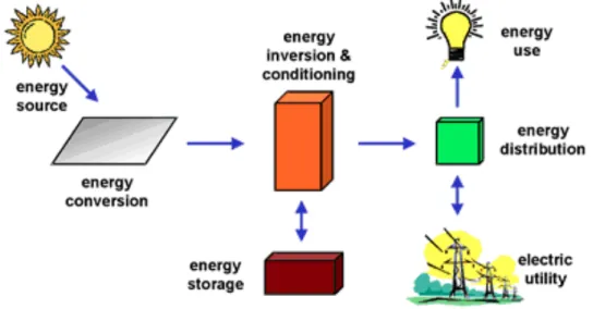
Although a PV array produces power when exposed to sunlight, various different parts are required to appropriately lead, control, convert, convey, and store the vitality created by the array.
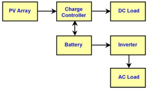
Dependent upon the useful and operational prerequisites of the framework, the particular segments required may incorporate significant segments, for example, a DC-AC control inverter, battery bank, framework and battery controller, assistant vitality sources and once in a while the predetermined electrical burden (apparatuses). Likewise, a combination of balance of system (BOS) equipment, including wiring, overcurrent, flood assurance and disengage gadgets, and other power preparing gear [4]. Figure below demonstrate a fundamental graph of a photovoltaic framework and the relationship of individual segments.
13
3.5 For what reason Are Batteries Used in Some PV Systems?
Batteries are frequently utilized in PV frameworks to store vitality delivered by the PV cluster during the day, and to supply it to electrical loads as required (during the night and times of cloudy weather). Different reasons batteries are utilized in PV frameworks are to work the PV exhibit close to maximum power point, to control electrical burdens at stable voltages, and to supply flood flows to electrical burdens and inverters. Much of the time, a battery charge controller is utilized in these frameworks to shield the battery from cheat and over discharge.
3.6 Types of PV Systems.
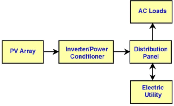
Photovoltaic power frameworks are by and large grouped by their practical and operational requirements, their segment designs, and how the gear is associated with other power sources and electrical burdens. The two head groupings are matrix associated or utility-intuitive frameworks and remain solitary frameworks. Photovoltaic frameworks can be intended to give DC as well as AC power administration, can work interconnected with or autonomous of the utility lattice, and can be associated with other vitality sources and vitality stockpiling frameworks.
Grid-connected or utility-interactive PV frameworks are intended to work in parallel with and interconnected with the electric utility lattice. The essential segment in network associated PV frameworks is the inverter, or power computing unit (PCU). The PCU changes over the DC power created by the PV exhibit into AC control predictable with the voltage and power quality prerequisites of the utility lattice, and naturally quits providing capacity to the matrix when the utility network isn't invigorated. A bi-directional interface is made between the PV framework AC yield circuits and the electric utility system, commonly at an on location circulation board or administration entrance. This permits the AC power delivered by the PV framework to either supply nearby electrical burdens, or to back-feed the matrix when the PV framework yield is more prominent than the on location burden request. Around evening time and during different periods when the electrical burdens are more
14
prominent than the PV framework yield, the level of influence required by the heaps is gotten from the electric utility This wellbeing highlight is required in all network associated PV frameworks, and guarantees that the PV framework won't proceed to work and criticism into the utility lattice when the matrix is down for administration or fix.
Figure 3.4: Diagram of grid-connected photovoltaic system 3.6.1 Stand-alone Photovoltaic Systems
Stab-alone PV frameworks are intended to work autonomous of the electric utility lattice, and are commonly structured and estimated to supply certain DC and additionally AC electrical burdens. These sorts of frameworks might be controlled by a PV cluster just, or may utilize wind, a motor generator or utility power as a helper power source in what is known as a PV-half breed framework. The easiest sort of remain solitary PV framework is a direct-coupled framework, where the DC yield of a PV module or exhibit is legitimately associated with a DC load. Since there is no electrical vitality stockpiling (batteries) in direct-coupled frameworks, the load just works during daylight hours, making these structures reasonable for normal applications, for example, ventilation fans, water siphons, and little course siphons for sun oriented warm water warming frameworks. Coordinating the impedance of the electrical burden to the greatest power yield of the PV cluster is a basic piece of planning admirably performing direct-coupled framework. For specific loads, for
15
example, positive-uprooting water siphons, a kind of electronic DC-DC converter, called a greatest power point tracker (MPPT), is utilized between the cluster and burden to help better use the accessible exhibit most extreme power yield.
Figure 3.5: Direct-coupled PV system
In many independent PV frameworks, batteries are utilized for vitality stockpiling. Figure above demonstrates an outline of a run of the mill remain solitary PV framework driving DC and AC loads. Figure 4 shows how a commonplace PV cross breed framework may be designed.
Figure 3.6: Diagram of stand-alone PV system with battery storage powering DC and AC loads
16
17
4. PROPOSED NEW HYBRID BF/F MICRO INVERTER
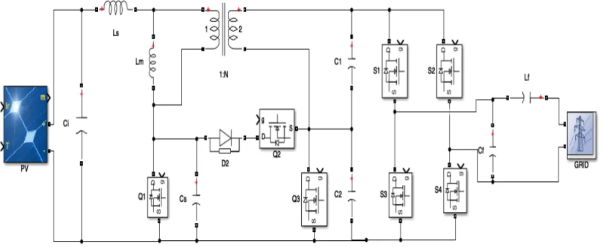
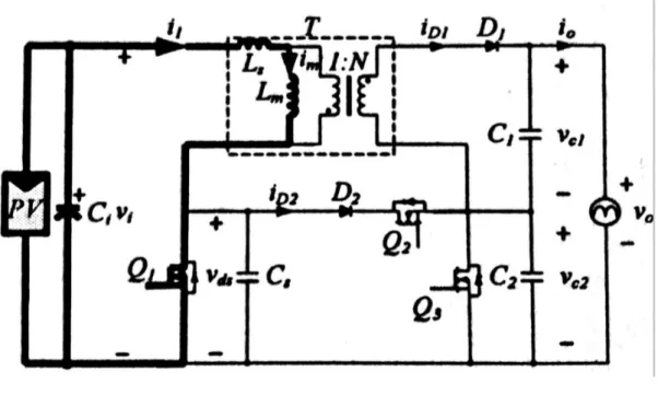
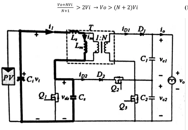
In figure 3 the proposed hybrid BF/F micro-inverter with non-isolated pseudo-dc-link, which comprises of a hybrid BF/F converter and an unfolding stage. the converter contains a decoupling capacitor Ci, a fundamental power switch q1, a resonant capacitor cs, two power rectifier diodes d1 and d2, two yield filter capacitors c1 and c2, a coupled transformer T that is demonstrated as a magnetizing inductor Lm, a leakage inductor Ls, and an ideal transformer with the turns ratio n, and an activity mode change arrange that is made out of two switches q2 and q3 complementarity worked at double-line frequency. The unfurling stage incorporates four switches s1, s2, s3 and s4 worked at line frequency, a filter capacitor Cf and a filter inductor Lf. In the event that the Switch Q2 is ON and Q3 is OFF, at that point the micro-inverter is in bf mode, generally, the micro-inverter is in F mode.
Figure 4.1: Proposed New Hybrid Bf/F Micro Inverter 4.1 Flyback inverter operated in different conduction modes
The BCM activity with pinnacle current control is embraced, since it offers high power density and change efficiency, it likewise gives natural soft-switching of power devices, counting ZVS and VS of the primary switch Q1, and ZCS of the
18
rectifier diodes D1 and D2, with the QR method utilized the micro inverter works at BF mode when Vo > Vi + V, outlined in figure 4.1, where Vo is the output voltage of the circuit, Vi is the normal estimation of the input voltage Vi, and ∆V is a consistent voltage value. During this mode, the switch Q2 is continuously ON and the Q3 is OFF, which makes the sub-booster converter successfully share the high instantaneous power with the sub-flyback converter. the boost inductor and the flyback transformer are coupled into the transformer T, and the yield voltage Vo is obtained by falling the output voltages (Vc1, Vc2) of the two sub-converters. Subsequently, high voltage addition is accomplished with low voltage stress on the principle switch Q1, the two rectifier diodes D1 and D2, and the two output capacitors C1 and C2. Then again, this mode inalienably gives a passive snubber, which is made of the Diode D2, and the Capacitors Cs and C2. Consequently, the energy stored in the leakage inductor Ls is reused to the Output side. Meanwhile, the voltage overshoot of the main switch Q1 is stifled during the Turn-Off procedure. Since the Output Voltage Vo can't be controlled Lower than the Input Voltage Vi during the BF Mode, the F Mode is created with the Switch Q3, Always ON and the Q2 OFF, This Mode is around the Zero Grid Voltage, where the Instantaneous moved Power is low. Therefore, the impact of the leakage Inductor can be disregarded. However, because of the way that the Switching Frequency during this Mode is very higher than the BF Mode, its duration which is determined by ∆V, should be fittingly confined to the shortest Possible Time.
The Resonant Capacitor Cs is included parallel with the fundamental switch Q1 for offering a proper QR time. It enables the Time to defer the Turn-on Driving Signal be structured flexibly, with the goal that the ZVS or on the other hand VS Turn-on in BCM activity is Guaranteed. Besides, this capacitor successfully improves the turn-off procedure by bringing down the rising slope of the voltage across Q1.
4.2 Operating Technique
In light of the photovoltaic idea of solar panels, their current-voltage, or IV, curves rely upon temperature and irradiance levels. Along these lines, the
19
working current and voltage which maximum power yield will change with ecological conditions. As the ideal point changes with the normal conditions so it is critical to follow the maximum power point (MPP) for a fruitful PV system. So in PV frameworks a most maximum power point tracker (MPPT) is particularly required. In most PV frameworks a control algorithm, to be specific maximum power point tracking algorithm is used to have the full preferred position of the PV systems.
For some random arrangement of operational conditions, cells have a solitary working point where the estimations of the current (I) and voltage (V) of the cell bring about a greatest power yield. These qualities compare to a specific load resistance, R= V/I, as indicated by Ohm's Law. The power P is given by P = V*I. From fundamental circuit theory, the power conveyed from or to a device is improved where the subsidiary of the I-V curve is equivalent and inverse the I/V ratio. This is known as the maximum power point (MPP) and corresponds to the "knee" of the curve.
The load resistance R=V/I, which is equivalent to the complementary of this worth and draws the maximum power from the device is some of the time called the characteristic resistance of the cell. This is a powerful amount which changes relying upon the intensity, just as different factors, for example, temperature and the age of the cell. In the event that the resistance is lower or higher than this worth, the power drawn will be not exactly the maximum accessible, and along these lines the cell won't be utilized as productively as it could be. Maximum power point trackers use various sorts of control circuit or logic to look for this point and along these lines to permit the converter circuit to remove the greatest power accessible from a cell
20
Figure 4.2: Key waveforms of the new micro-inverter in BCM 4.3 Operating Principle
The BF/F Micro-Inverter incorporates five particular activity modes, as portrayed in the Figure 5, when worked at BF Mode during one switching period Ts. figure 4.2 outlines the equal Circuits of every activity Mode, where the Switch Q2 remains consistently ON, and the Q3 OFF. It is to be noticed that the unfurling stage and the grid are supplanted with a rectified sinusoidal voltage source for disentangling the examination. Moreover, the parasitic capacitor of the primary switch Q1 is considered into the Resonant Capacitor Cs, and the Voltages Vi , Vc1, Vc2, Vo and the reference Current Irei_BF are thought to be consistent
21
Figure 4.3: Operating waveforms under BF mode Mode I (T0-T1)
The switch Q1 has been turned on before time T0. The primary current I1, flowing through the leakage inductor Ls and the magnetizing inductor Lm, increments Linearly with the pace of (%&'%()"# . When it arrives at the reference Current 𝐼𝑟𝑒𝑓_𝐵𝐹, the switch Q1 is off and this mode end.
22
Figure 4.4.1: Mode I (T0-T1)
Mode II (T1-T2)
During this mode, resonance happens and the inductor is considered large the essential current I1 remains practically constant (𝐼𝑟𝑒𝑓_𝐵𝐹) in this time interval. As an outcome, the drain-to-source voltage of Q1 increments straight with the rate of 𝐼𝑟𝑒𝑓_𝐵𝐹/𝐶𝑠, demonstrating that the expansion of Cs successfully diminishes the rising Slope of the voltage 𝑉𝑑𝑠. This mode closes at time T2, where the 𝑉𝑑𝑠 comes to (𝑉𝑜 + 𝑁𝑣𝑖)/(𝑁 + 𝐼).
23
Figure 4.4.2: Mode II (T1-T2) Mode III (T2-T3)
At time T2, the output rectifier diodes D1 and D2 are forward biased. On the ideal condition with the leakage inductance ignored, the Diode currents 𝑖𝐷1 and 𝑖𝐷2 decline all the while from 𝐼𝑟𝑒𝑓_𝐵𝐹/(𝑁 + 1) to Zero with a similar pace of 𝑉𝑐1/𝑁@ ∗ 𝐿𝑚. Consequently, the reverse-recovery issue of D1 and D2 can be solved. Then, the voltage Vds keeps up the consistent estimation of (𝑣𝑜 + 𝑁𝑣𝐼)/(𝑁 + 𝐼) during this interval. Nonetheless, there Occurs a high-frequency resonance entirely the leakage Inductor (Ls) and the Capacitors (Cs, C2) at the start of this mode, as appeared in the spotted Waveforms of figure 5. It makes the voltage stress of the switch Q1 diminished and the energy of leakage inductor Ls reused.
24
Figure 4.4.3: Mode III (T2-T3) Mode IV (t3-t4)
This mode is like mode II, where the reverberation happens again between the Inductors (Lm, Ls) and the Capacitor (Cs). The Voltage Vds step by step rots towards zero if the condition appeared in Equation (1) is fulfilled
"D'E"#
E'F > 2𝑉𝑖 → 𝑉𝑜 > (𝑁 + 2)𝑉𝑖 (1)
25 The time of this mode is half resonance period,
Shown in the 2nd equation which should not be bigger than time delay Td
𝑡34 = 𝜋N(𝐿𝑚 + 𝐿𝑠). 𝐶𝑠 (2) Mode V(t4-t5)
After the passing of t4, Current I1 flows negative through diode Q1, the voltage across Q1 is clamped at zero. Then Q1 is applied and ZVS turn-on is achieved.
Figure 4.4.5: Mode V(t4-t5) 4.4 Proposed Reference Current
In BCM mode at peak current control. The average output Io, regarded as absolute value of the current in the grid, the mathematical precession between Iref and Io turns out to be amazingly critical.
In the Hybrid BF/F micro-inverter, the ideal reference current of F Mode can be altered as
𝐼𝑟𝑒𝑓_P = 2. 𝐼𝑜. ("D"# + 𝑁) (3) About the impact of the leakage inductor and the QR time, a progressively precise reference Current of F Mode is introduced. Be that as it may, it is too muddled to ever be applied to Advanced Calculation. Also, the impact of these
26
non, Perfect variables can be limited by improving the equipment structure. The two reasons as referenced above Is too valid for the BF Mode, subsequently invigorating just the perfect reference Current to be researched in this paper. Preceding inferring the formula of the BF mode reference Current 𝐼𝑟𝑒𝑓_𝐵𝐹, a few assumptions ought to be made as pursues:
a) During One Switching period Ts, Vi, Vc1, Vc2, V0 and 𝐼𝑟𝑒𝑓_𝐵𝐹 are considered as constants.
b) All the Power devices including Q1, Q2, Q3, D1 and D2 are ideal without parameters into account.
C)The coupled Transformer T should be ideal and the resounding capacitor Cs is barred, therefore the impact of the leakage inductor Ls and the Time term (t12, t34) can be overlooked.
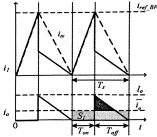
During the turn-on interval in each switching cycle, as delineate in figure 6 the polarizing current Im increments linearly from zero to its pinnacle esteem Iref_BF and the turn-on time Ton can be expressed as
𝑇𝑜𝑛 = 𝐼𝑟𝑒𝑓SP.%&"# (4) while in the turn-on period the magnetizing current Im diminishes linearly until it reaches to zero and can be given as
𝐼𝑚 = 𝑁𝐼𝑑𝑖 + 𝐼𝑑2. (5) The relationship of Io, Id1 and Id2 is
𝐼𝑜 = 𝐼𝑑1 = 𝐼𝑑2 (6) the equation (5) can be altered as
27
Figure 4.5: Waveforms of primary and output current under BF mode
where Io is the pinnacle estimation of Io, besides the Turn-on Time Toff can be gotten
𝑇𝑜𝑓𝑓 = 𝐼𝑜.E"UFT.%& (8) in light of the relentless state investigation of the BF converter the after condition can be determined:
𝑉𝑜 =F'E.VFWV . 𝑉𝑖 → 𝐷 ="D'EX#"DW"# (9) 𝑉𝑐1 =FWVE.V. 𝑉𝑖 (10) where D is the duty cycles under BCM activity. Substituting (9) to (10) the condition (10) is altered as
28
Agreeing to the law of proportionate territory, the rectangular zone S1 is roughly equivalent to the triangle zone S2. Thus the normal Output current Io can be gained as
𝐼𝑜 =
Y T.ZD.[D\\
[D]'[D\\ (12) assembling every one of the recipes 𝐼𝑟𝑒𝑓 is acquired as
𝐼𝑟𝑒𝑓 = ^2. 𝐼𝑜 _ E'F E . "DW"# "İ + (𝑁 + 1)a , 𝐵𝐹 2. 𝐼𝑜. _"D"#. 𝑁a , 𝐹 c (13)
29
5. DESIGN CONSIDERATION AND CHARACTERISTIC ANALYSIS
5.1 The below figure is the main circuit which shows the micro-inverter
Figure 5.1: Proposed new micro-inverter 5.1.1 Solar Panel Design
The PV Array block executes a variety of photovoltaic (PV) modules. The exhibit is worked of series of modules connected in parallel, each string comprising of modules associated in arrangement. The PV Array block is a five parameter model utilizing a current source IL (light-produced current), diode (I0 and nI parameters), series resistance Rs, and shunt resistance Rsh for the irradiance-and temperature of the I-V attributes of the modules [5].
30
The output vector containing five output signal from the solar panel module in the table below
Table 5.1: Parameters of solar panel module
Signal Signal Name Definition
1 V_PV Pv array voltage (V)
2 I_PV Pv array current (A)
3 I_diode diode current (A)
4 Irradiance (W/m2) Irradiance (W/m2)
5 Temperature (deg C) Temperature (degrees C)
5.1.2 Hybrid BF/F Converter
The figure below is the stage of the hybrid BF/F converter, this is the stage where the circuit switches from BF to F mode the stage contains the transformer the two power rectifier diodes, the MOSFET and the two switches that operate on double line frequency.
31 5.1.3 Unfolding stage
The figure below shows the unfolding stage which includes four switches s1, s2, s3, s4 operated on line frequency, a filter Cf capacitor and a filter inductor Lf.
Figure 5.4: Unfolding stage of the converter 5.1.4 Grid
The grid has the load parameters connect to is in table 5.2, the value of the parameters are changes based on different types of loads.
Table 5.2: Parameters of load
Parameters Symbols
Resistor 1 R1
Resistor 2 R2
32
Figure 5.5: The grid with load 5.1.5 Control panel
The control circuit contains two part which are: I. The MPPT
II. The Unfolding stage I. The MPPT
Photovoltaic system for the most part utilize a Maximum power point tracking (MPPT) system to remove greatest conceivable power from the PV module independent of the perturbation in insolation and temperature. PV modules have generally low change proficiency; subsequently it requires MPPT method for controlling the solar power. The Maximum Power Point Tracking (MPPT) is a method for which most maximum power can be extracted from the Photovoltaic (PV) Systems. To improve the energy effectiveness, it is applicable to work the all out PV module consistently at its greatest power point. Numerous most maximum power point Tracking (MPPT) methods are accessible in the present time and among every one of these procedures P&O and gradual conductance calculations are commonly utilized in PV system for getting maximum power point [6].
33
Figure 5.6: Structure of MPPT II. The Unfolding stage
At the unfolding stage of the control circuit, the circuit contains the components below;
I. PLL II. PID III. PWM
Figure 5.7: Structure of PLL 1. Phase Lock Loop (PLL)
The PLL block models a Phase Lock Loop (PLL) circle control framework, which tracks the frequency and period of a sinusoidal sign by utilizing an interior frequency oscillator. The control framework changes the inside oscillator frequency to keep the phase difference to 0.
34
The input sign is blended with an inward oscillator signal. The DC segment of the mixed sign (corresponding to the phase contrast between these two signals) is separated with a variable frequency mean value. A Proportional-Integral-Derivative (PID) controller with a automatic gain control (AGC) keeps the phase contrast to 0 by following up on a controlled oscillator. The PID yield, comparing to the angular velocity, is sifted and changed over to the frequency, in hertz, which is utilized by the mean value.
The has PLL input IN and the outputs are Freq (measured frequency in hetz) and wt (angle (rad) varying between 0 and 2*pi)
Figure 5.8: The internal diagram of PLL 2. PID
PID (Proportional Integral Derivative) controllers are the most generally utilized controllers in modern settings due to their usability and the fulfilment of execution they are skilled to give the client to an enormous number of procedures. Despite the fact that the cost/advantage proportion gave by these controllers is far more than given by some other controller. Numerous systems have been proposed for their structure, in view of their across the board use, for the tuning of the parameters of PID i.ie Kp, Ki and Kd and for the execution of extra functionalities that improve their exhibition.
35
Figure 5.9: The PID system block A PID controller is made up of a three section:
1. Proportional compensation: the fundamental capacity of the corresponding compensator is to present an increase that is corresponding to the blunder perusing which is created by contrasting the framework's yield and info.
2. Derivative compensation: in a unitary criticism framework, the subordinate compensator will present the subsidiary of the mistake sign duplicated by an increase KD. At the end of the day, the slant of the blunder sign's waveform is the thing that will acquainted with the yield. Its fundamental reason for existing is that of improving the transient reaction of the general shut circle framework. 3. Integral compensation: in a unitary input framework, the necessary compensator will present the basic of the mistake sign duplicated by an addition KI. This implies the zone under the blunder sign's bend will influence the yield signal. We will demonstrate this later, however note that this feature of the controller will improve the unfaltering state blunder of in general shut circle framework.
36 Table 5.2: Mathematical expressions of PID
Therefor PID can be express mathematically as below:
Figure 5.10: internal circuit of PID controller in the controller 3. PWM
Pulse width regulation (PWM), or pulse duration modulation (PDM) is a tweak system that accommodates the width of the pulse, officially the pulse length, in view of a modulator signal data. In spite of the fact that this regulation procedure can be utilized to encode data for transmission, its fundamental use is to permit the control of the power provided to electrical gadgets, particularly to inertial loads, for example, engines. The normal estimation of voltage (and current) sustained to the heap is constrained by turning the switch among inventory and burden on and off at a quick pace. The more drawn out the switch is on contrasted with the off periods, the higher the power provided to the load is. The PWM exchanging frequency must be a lot quicker than what might influence the load, or, in other words the gadget that uses the power. Normally
37
switching must be completed a few times each moment in an electric stove, 120 Hz in a light dimmer, from couple of kilohertz (kHz) to many kHz for an engine drive and well into the tens or several kHz in sound intensifiers and PC power supplies.
The term duty cycle portrays the extent of 'on' time to the standard interim or 'time' of time; a low obligation cycle compares to low power, in light of the fact that the power is off for more often than not. Obligation cycle is communicated in percent, 100% being completely on. The principle bit of leeway of PWM is that power misfortune in the exchanging gadgets is low. At the point when a switch is off there is for all intents and purposes no current, and when it is on, there is no voltage drop over the switch. Power misfortune, being the result of voltage and current, is in this manner in the two cases near zero. PWM likewise functions admirably with computerized controls, which, in view of their on/off nature, can without much of a stretch set the required obligation cycle. PWM has additionally been utilized in certain correspondence frameworks where its obligation cycle has been utilized to pass on data over an interchanges channel.
38
Figure 5.12: Shows the control circuit which contains the MPPT and unfolding controllers
5.2 Other components in circuit 5.2.1 Coupled Transformer a) Turns Ratio N
The voltage rating of the principle switch Q1 ought to be given First, along these lines the maximum output voltage 𝑉𝑐2. 𝑚𝑎𝑥 of the sub-boot converter can be affirmed with the leakage spike voltage and some edge thought about.
According to the connection between the input Vi and output Vc2 as
𝑉𝑐2 =FWVF . 𝑉𝑖 (14) the maximum Duty cycle Dmax can be calculated as
𝐷𝑚𝑎𝑥 = 1 −"U@.&gh"F.&#] (15) where Vi.min is the base estimation of input voltage Vi. At that point from (9), the turns ratio N is gotten as
𝑁 ="D.(FWV&gh) "#.&#].V&gh−
F
39
where Vo is the pinnacle estimation of the rectified sinusoidal output voltage Vo.
Then again, so as to guarantee the active safety of the micro-inverter, the most extreme hypothetical voltage over the principle switch Q1 during the F Mode should be checked as
𝑉𝑖. 𝑚𝑎𝑥 +"#.&gh'∆"E ≤ 𝑉𝑐2. 𝑚𝑎𝑥 (17) where Vt.max is the most extreme estimation of information voltage Vi.
b) Magnetizing Inductance Lm
The turn-on time Ton can likewise be communicated as
𝑇𝑜𝑛 =\(V (18) Fs is the switching frequency of Q1, the turn-off time, is given as
𝑇𝑜𝑓𝑓 =FWV\( (19) Putting all the formula together Lm is obtained as
𝐿𝑚 = F@.ZD\(.&#](F'E)(F'V&ghE)"DV&gh(FWV&gh)T (20) Io is peak value of rectified sinusoidal output current Io, fs.min is the minimum switching frequency of Q1
b) Capacitances Cs and C2
The capacitance Cs is planned primarily to coordinate the time delay Td, and its worth is determined from (2). Furthermore, it works as a snubber Capacitor together with the capacitance C2 in mode III. The estimation of C2 can be gotten
𝑉𝑠 = 𝐼𝑚. 𝑚𝑎𝑥. jk('k@%( → 𝐶2 =Z&.&gh"(TT.%(− 𝐶𝑠 (21) Where Vs is the spike voltage brought about by the reverberation between Ls and Cs, C2, and Im.max is the pinnacle magnetizing current.
40
Figure 5.13: Discharging conduction path for output capacitor C2
A moderately enormous estimation of C2 adequately limits the spike voltage, however builds the reverberation length during the turn-off process, therefore lessening the efficiency besides, huge estimation of C2 would influence the progress from BF to F mode and the rectified sinusoidal waveform of output voltage Vo. In this way, the capacitance C2 ought to be constrained to the least conceivable worth, as a rule arranged by nanofarads.
c) Transition Dead Time
The corresponding switches Q2 and Q3 are acquainted with understand the activity change between the BF and F mode during a half-line period, while in down to earth applications, the change dead time is utilized for keeping away from a short circuit so that the driving Signals of the two switches are not carefully corresponding.
Given that the switch Q3 is in parallel with the output capacitor C2, the change dead time ought not be smaller than the releasing time of C2 all together that the ZVS turn-on of Q3 is accomplished the minute the BF mode is travelled to
41
the F mode, what's more, the releasing conduction way for C2 is appeared in Figure 5.14.
d) Complementary Switches Q2 and Q3
The maximum voltage stress of the switch Q2 is equal to the maximum voltage across the main switch Q1 in F mode. With the leakage spike voltage
neglected, it can be calculated as
𝑉 𝑑𝑠_l@mno = 𝑉𝑖. max +"#.&gh'∆"E (22) The maximum current stress of the switch Q2 is obtained as
𝐼𝑞2. 𝑚𝑎𝑥 = 2. 𝐼𝑜. (EF."DW"#.&#]"#.&#] + 1) (23) The maximum voltage stress of the switch Q3 Vds_Q3.max equal to the maximum Sub-boost output voltage Vc2.max, and the maximum current stress is calculated as
𝐼𝑞3. 𝑚𝑎𝑥 = 2. 𝐼𝑜."#.&gh'∆""D . (EF."#.&gh'∆""#.&gh + 1) (24) Both Q2 and Q3 are operated at only double-line frequency, and the voltage and current stress of them are lower than those of the main switch Q1. However, they also participate in energy transmission inevitably, which will definitely diminish the efficiency of the micro-inverter. Thus, the MOSFETs with low On-resistance should be selected for minimizing the conduction
Losses.
e) Characteristic Analysis
Due to the fact that the switching frequency of the main switch Q1 will he significantly increased near the edges of the sinusoidal wave, the critical current Ic needs to be designed to prevent the micro-inverter from working if the average output current is lower than Ic. Moreover, the output voltage Vo and the average output current can be described as
42
Substituting (25) to (13), and thinking about the basic current Ic, the reference current iref of hybrid BF/F miniaturized scale inverter under BCM activity can be obtained as Iref = ⎝ ⎛ 2. Io _€'F€.•‚. sin@wt. + _N −F €a . sin wta , (wt2 < wt < wt3)
2. Io. _•‡•‚. sin@wt + N. sin wta , (wt1 < wt ≤ wt2 ∪ wt3 ≤ wt < wt4) 0 , (0 < wt ≤ wt1 ∪ wt4 ≤ wt < π) ⎠ ⎞ (26) Where wt1 = sinWF _F Œ‡a , wt2 = sin WF1[(Vi + ∆V/Vo)], Wt3 = π - sinWF [(V+∆V)/Vo)], wt4 = π − sinWF(Ic/Io).
Figure 15.14a, b,c show the characteristic curves of the micro-inverter
43 Figure 5.14.2: Switching frequency
Figure 5.14.3: Drain-to-source voltage
Considering the impact of QR time TQR, which can be altered from (2) with the spillage inductance disregarded as
44
the exchanging frequency of the primary switch Q1under BF mode can be described as
fs_BF =˜‡™'˜‡šš'˜›œF (28) Consolidating (4), (7), (8), (II), (13), (25), (27) and (28), the BF mode exchanging recurrence of Q1 can be at last gotten, at that point as per the switching frequency of F mode and dead band, the switching recurrence fs of hybrid BF/F small scale inverter can be closed as appeared in condition (29). Without considering the leakage spike voltage, the voltage over the primary switch Q1 of BF mode is equivalent to the sub-boost yield voltage Vc2. Consolidating (9), (14) and (25), the channel to-source voltage of Q1 in BF mode is gotten, at that point in light of the drain-to-source voltage both in F mode and dead band, the perfect drain-to-source voltage of Q1 is closed as
Vds = ž •‡Ÿ‚™ ¡'€¢‚ €'F , (wt2 < wt < wt3) •‡Ÿ‚™ ¡'€¢‚, € (wt1 < wt ≤ wt2 ∪ wt3 ≤ wt < wt4) Vi , (0 < wt ≤ wt1 ∪ wt4 ≤ wt < π) £ (30)
The characteristics curves down the middle line time frame for hybrid BF/F smaller scale inverter are delineated in strong lines as appeared in Fig. 8 by utilizing (26), (29) and (30) with Io=1.55A, Vo=311V, Vi= 35V, N=5, Cs=2.2nF, Lm=4.69uH, ∆V=30V, Ic=77mA. The micro inverter is worked at BF mode during 0.21 < wt < 2.93, while at F mode during 0 ≤ wt ≤ 0.21 or 2.93 ≤ wt ≤ π, where, the internal 0 ≤ wt ≤ 0.05 and 3.09 ≤ wt ≤ π P are dead band. Clearly, the BF mode possesses the most occupies most part of the period contrasted and the F mode.
As appeared in figure 15.4 (a), the reference current of BF mode is higher than that of F mode, and the reference current progresses toward becoming zero when entering dead band. Also, the reference current is ceaseless at the mode change point 0.21 or 2.93, which implies that the smooth progress among BF and F mode is accomplished normally. From (29), the entire switching frequency range can be determined accurately as 92.4~586.6 kHz with the dead band disregarded, in which the exchanging recurrence scope of BF mode is 92.4~234.9 kHz, and the scope of F mode is 397.2~586.6 kHz. It is all the more
45
intriguing that, as appeared in figure 15.4 (b), the most extreme switching frequency of BF mode isn't at the progress point 0.21 or 2.93 yet at 0.27 or 2.87, and the exchanging recurrence at the change point is simply 222.7 kHz. Additionally, the exchanging recurrence is discrete at the progress point, where the switching frequency abruptly moves from 397.2 kHz at F mode to 222.7 kHz at BF mode, and the other way around. Figure 15.4 (c) demonstrates that the channel to-source voltage of BF mode is sinusoidal, also, that of F mode is sinusoidal too separated from the dead band. Be that as it may, there happens an unexpected voltage change at the change point. The channel to - source voltage drops from 48V to 4OV when the F Mode is travelled to BF Mode, and the other way around Through the examination with the normal for flyback miniaturized scale inverter under similar parameters, as appeared in the dabbed lines of figure 15.4, it is seen that both Micro-Inverters carry on in an equivalent manner during 0< WT < 0.21 or 2.93 < WT < π, while perform contrastingly during 0.21 < WT < 2.93, where the reference current for hybrid BF/F micro-inverter is higher than that of flyback micro-inverter, notwithstanding, the switching frequency and the drain-to-source voltage play out the inverse status. In this interval, the switching frequency extend and the most extreme drain-to-source voltage of flyback micro-inverter are 107.1 ~397.2 kHz and 97.2V, individually, while those of smaller scale Inverter are just 92.4-234.9 kHz and 81V.
47 6. SIMULATION RESULTS.
The simulation, as appeared in figures below was set up using MATLAB Software to validate the proposed new hybrid BF/F micro-inverter. The Circuit Parameters are recorded in Table 6.1 for the first simulation, also, the Control Scheme are done by the S-work Mode.
For the simulation the below parameters are used. Table 6.1: Circuit Parameters
Parameters Symbols Value
Output Po 240w
Input Voltage VI 22-49W
Grid Voltage Vg 220Vrms
Grid Frequency F-line 60Hz
Constant Voltage ∆ V 30V
Input Capacitance Ci 4*3300UF
Magnetizing Inductance Lm 4.69uH
Leakage Inductance Ls 60nH
Resonant Capacitance Cs 2.2nF
High Side Output Capacitance
C1 22nF
Low Side Output Capacitance
C2 6.8nF
Output Filter Inductance Lf 2mH
Output Filter Capacitance
Cf 220nF
Irradiance I 1000
48
For the Pv panel the figure below shows the graph for specific temperature temperature
Figure 6.1: Shows current and power for the Pv panel module
Figures show the key wave forms of the simulation done for the new micro-inverter,35v as the input with full load conditions. Currrent is injced to the circuit and modulate as shown in the below figure it is a smooth sinusoidal waveform as expected, the output volatge is Vo is a rectified sinusoidal waveform gotten by the superposition of the sub-flyback voltage Vc1 and Vc2. And it has the same phase as the grid voltage Vg.
49
Figure 6.2: Wave forms of Vo
50
Figure 6.4: Waveforms of VC1 and VC2
The figure below shows the complementary driving signal wave forms of the switches Q1, Q2, Q3in which Q2 and Q3 operate on double line frequency of 120Hz and the two switches transition between BF and F mode
Figure 6.5: The switches Q1at line frequency and at double line frequency (120Hz) Q,2Q3,
51
For figure below is shows the the continuous envelope of I1 the primary current and sinusoidal wave forms of the output diode current Id1 and Id2 where Id2 has a little more distortion due to the effect of the leakage inductor energy. And also the primary current of Id1 in Bf mode is different from Id2 in F mode because there is output diode current in Id2.
Figure 6.6.1: Waveforms of Id1
Figure 6.6.2: Waveforms Id2
The below figure show the wave forms of the voltage of Q1 drain to source voltage (Vds), the switching frequency of the main switch is in BF mode is lower than in F mode
52
Figure 6.7: Grid output voltage and current waveforms 6.1 Comparism between inverters
Below is a comparism between three converters from three publications:
1) The the converter from [7] research paper is compared to the the new micro-inverter discussed in this thesis the results are as follow
53
Figure 6. 9: Output voltage of result of Single-Stage Grid-Connected Flyback Microi-nverter
2) The second inverter compared to the new micro inverter is [8], below is the circuit and the output waveforms of the inverter
Figure 6.10: Circuit diagram of Photovoltaic flyback micro-inverter with power decoupling technique