Dielectric screening effects on electron transport in
Ga0.51In0.49P/InxGa1−xAs/GaAs quantum wells
C. Besikci, A. T. Bakir, and B. Tanatar
Citation: J. Appl. Phys. 88, 1504 (2000); doi: 10.1063/1.373846
View online: http://dx.doi.org/10.1063/1.373846
View Table of Contents: http://jap.aip.org/resource/1/JAPIAU/v88/i3
Published by the American Institute of Physics.
Additional information on J. Appl. Phys.
Journal Homepage: http://jap.aip.org/
Journal Information: http://jap.aip.org/about/about_the_journal
Top downloads: http://jap.aip.org/features/most_downloaded
Dielectric screening effects on electron transport
in Ga
0.51In
0.49P
Õ
In
xGa
1ÀxAs
Õ
GaAs quantum wells
C. Besikcia)and A. T. Bakir
Electrical Engineering Department, Middle East Technical University, 06531 Ankara, Turkey B. Tanatar
Department of Physics, Bilkent University, 06533 Ankara, Turkey
共Received 13 December 1999; accepted for publication 18 April 2000兲
The effects of dielectric screening on the two dimensional polar optical phonon scattering and on electron transport in Ga0.51In0.49P/InxGa1⫺xAs/GaAs (x⫽0, 0.15, and 0.25兲 modulation doped
heterostructures and high electron mobility transistors are investigated through the ensemble Monte Carlo technique. The two dimensional polar optical phonon scattering rates including and excluding dielectric screening effects are calculated using the self-consistently evaluated electronic states in the quantum well. The calculated scattering rates are compared in order to see the effects of screening on the inter- and intra-subband scattering. Screening significantly lowers the intra-subband polar optical phonon scattering rates in both lattice matched and pseudomorphic structures. This results in a considerable lowering of the critical electric field beyond which negative differential resistance is seen. Screening also modifies the dependence of transport properties on the quantum well parameters. The results of the ensemble Monte Carlo simulations of high electron mobility transistors show that the performance of the device is considerably underestimated, if screening is not included in the calculation of the polar optical phonon scattering rates. © 2000
American Institute of Physics. 关S0021-8979共00兲00515-6兴
I. INTRODUCTION
III–V heterostructures have widely been used for high performance electron devices such as high electron mobility transistor共HEMT兲 and optical devices such as quantum well photodetectors and lasers. AlGaAs is the most commonly used large band gap material for heterostructure devices on GaAs substrates. However, due to the well known advan-tages of GaInP over AlGaAs,1this material has recently re-ceived increasing attention to replace AlGaAs,2–6 and high performance Ga0.51In0.49P/InxGa1⫺xAs/GaAs HEMTs have
been demonstrated.
In order to use the desirable transport properties of the two dimensional electron gas共2DEG兲 efficiently in quantum well devices such as HEMTs, one must have a sound under-standing of the physics of carrier transport in 2D systems. Phonon, impurity, and alloy scattering mechanisms in 2DEG have been studied7–12and the 2DEG velocity-field character-istics in modulation doped heterostructures have been inves-tigated through Monte Carlo simulations.13–16 There have been many efforts to develop an accurate model for HEMTs. A review of these models was presented by Salmer et al.17 The Monte Carlo technique has been the most accurate and complete method for the simulation and optimization of HEMTs.18–20 However, some mechanisms, which are as-sumed to be of second order, such as screening in polar optical phonon 共POP兲 scattering, were ignored in the previ-ous device simulations. Screened electron–polar optical pho-non interaction has been investigated by Price21 and Basu
and Kundu.22In this article, we present the results of precise Monte Carlo simulations of 2D electron transport in Ga0.51In0.49P/InxGa1⫺xAs/GaAs modulation doped structures
and in HEMTs including the effects of dielectric screening in order to show the importance of screening effects. While the simulations performed in this work are for the Ga0.51In0.49P/InxGa1⫺xAs/GaAs heterostructures, main con-clusions of the article should also be valid for modulation doped structures based on other material systems.
Our Monte Carlo simulation programs consider the low-est three subbands in the quantum well,⌫, L, and X valleys of the conduction band and all the dominant 2D and 3D scattering mechanisms. In order to increase the accuracy of the results, trial subband wave functions are not used and the electronic states in the quantum well are calculated self-consistently by coupling the Schro¨dinger and Poisson’s equations. Two dimensional scattering rates are calculated using the obtained results for the electronic states. The re-sults of our work clearly show that POP screening should be taken into account in device Monte Carlo simulations in or-der to predict the dc and high frequency performance of the device correctly.
The procedure for calculating the quantum well elec-tronic states is briefly presented in Sec. II. Section III de-scribes the calculation of the 2D POP scattering rates includ-ing the dielectric screeninclud-ing effects and discusses the effects of screening on the inter- and intra-subband POP scattering. Effects of screening on the transport properties of the hetero-structures are given in Sec. IV. Section V presents the results of HEMT ensemble Monte Carlo simulations and investi-gates the effects of screening on the device performance
pre-a兲Electronic mail: [email protected]
1504
dicted by the simulations. Concluding remarks are given in Sec. VI.
II. QUANTUM WELL ELECTRONIC STATES
The electronic states in the Ga0.51In0.49P/InxGa1⫺xAs/ GaAs modulation doped heterostructures with various chan-nel In mole fraction (x), InGaAs layer thickness and barrier
共GaInP兲 layer doping are calculated self-consistently by
solv-ing the Schro¨dsolv-inger equation ussolv-ing the Numerov method.23 Assuming that the wave function parallel to the heterointer-face (x y plane兲 is in the form of a plane wave, Schro¨dinger equation for the envelope wave function for subband m
关⌿m(z)兴 normal to the heterointerface can be expressed as
⫺ ប
2
2m*
d2⌿m共z兲
dz2 ⫹V共z兲⌿m共z兲⫽Em⌿m共z兲, 共1兲
where V(z) is the effective potential.24 When the lowest three subbands in the quantum well are taken into account, Poisson’s equation in the quantum well reads
d2U共z兲 dz2 ⫽ e ⑀
冋
i兺
⫽1 3 ni⌿i 2共z兲⫺N D共z兲⫹NA共z兲册
, 共2兲 where U(z) is the electrostatic potential, ND(z) is the ion-ized donor density, NA(z) is the ionized acceptor density, and niis the density of electrons in subband i found fromni⫽
m*kT
ប2 ln
冋
1⫹ exp冋
EF⫺Ei
kT
册册
. 共3兲The coupled Eqs. 共1兲–共3兲 are solved using the Numerov method. The Fermi–Dirac integral is also solved in degener-ate regions of the heterostructures in order to establish a relation between the electron density and the Fermi level. A self-consistent solution procedure is carried out along 1500 mesh points distributed throughout the heterostructure.
Figure 1 shows the calculated subband wave functions at 77 K for the lattice matched GaInP/GaAs heterostructure with a GaInP共barrier兲 layer donor doping of 2⫻1018cm⫺3. The energy levels at this temperature are found to be 88, 130, and 146 meV, respectively for the lowest three subbands.
III. 2D POLAR OPTICAL PHONON SCATTERING RATES
For a three-subband model, the polar optical phonon scattering rates are calculated using the Fermi’s Golden Rule7,25 ⌫i j共k兲⫽ e2wLO 2
冉
nB共wLO兲⫹ 1 2⫾ 1 2冊
⫻冕
d2qHjii j eff共q兲 q ␦关Ei共k兲⫿បwLO⫺Ej共k⫿q兲兴, 共4兲where the upper and lower signs refer to the emission and absorption processes, respectively. nB(wLO) is the Bose dis-tribution function giving the average number of phonons with energyបwLOat temperature T. Dielectric screening ef-fects are taken into account within a static approximation by considering an effective interaction Heffdefined in terms of the dielectric matrix25
Hi jkl共q兲⫽
兺
mn ⑀i jnm共q,w⫽0兲Hmnkl
eff 共q兲. 共5兲
In the absence of screening, the subband form factors are expressed by Hi jkl共q兲⫽
冕
0 ⬁ dz冕
0 ⬁ dz⬘
e⫺q兩z⫺z⬘兩⌿i共z⬘兲⌿j共z⬘兲⌿
k共z兲⌿l共z兲 共6兲in which the self-consistently calculated wave functions are used. The dielectric matrix embodying the screening effects is given in the random phase approximation by
⑀i jnm共q兲⫽␦im␦jn⫺Vi jnm共q兲nm共q兲, 共7兲 where nm(q) is the static polarizability. The form factors and the Coulomb interaction matrix elements are related by
Hi jkl(q)⫽Vi jkl(q)/(2e2/q). In this work, we consider only the static dielectric function. The dynamical effects25 worthy of a separate study are beyond the scope of the present calculation. The matrix elements of the static dielec-tric function⑀(q) are calculated by keeping the full tempera-ture dependence. The usual Thomas–Fermi screening corre-sponds to the q→0 limit of our dielectric function. The static screening approximation adopted here should be appropriate for large carrier densities, since បwLO remains small
com-pared with the characteristic energy共i.e., plasmon energy兲 of the electron gas. The typical sheet electron densities in these heterostructures are usually larger than 1⫻1012cm⫺2 for
electron device applications. In all the structures investigated in this work, two dimensional electron density is higher than this value.
In the calculation of the 2D scattering rates in the het-erostructure quantum wells, approximate wave functions are commonly used. A single modulation doped heterostructure is usually approximated by a simple triangular quantum well and trial wave functions are used.26 However, this approach may result in a large error in the calculated 2D scattering rates. In order to investigate the error introduced by this ap-proach, we compared the 2D polar optical phonon scattering
FIG. 1. 77 K wave functions in the Ga0.51In0.49P/GaAs structure with a
barrier layer doping of 2⫻1018cm⫺3. Energy levels for the lowest three subbands are 88, 130, and 146 meV, respectively.
1505
rates obtained using trial wave functions with those calcu-lated by the exact wave functions. The exact wave functions were calculated self-consistently in the Ga0.51In0.49P/GaAs single quantum well with Ga0.51In0.49P layer donor doping of 2⫻1018cm⫺3. For comparison, we used the following trial
wave functions based on a variational approach:
1共z兲⫽共b3/2兲1/2z exp共⫺bz/2兲, 共8兲
2共z兲⫽共3b
3/2兲1/2z共1⫺bz/3兲exp共⫺bz/2兲, 共9兲
3共z兲⫽共3b3兲1/2z共1⫺2bz/3⫹b2z2/12兲exp共⫺bz/2兲, 共10兲
where the parameter b⫽(33m*e2N
s/⑀0)1/3 is related to the
sheet electron density, Ns. Figure 2 shows the 2D polar op-tical phonon emission and absorption rates in the second subband. Especially the intrasubband scattering rates in this subband are greatly underestimated, if the trial wave func-tions are used. Therefore, we used the self-consistently cal-culated wave functions to obtain reasonable accuracy in the calculation of the transport in the heterostructures investi-gated in this work.
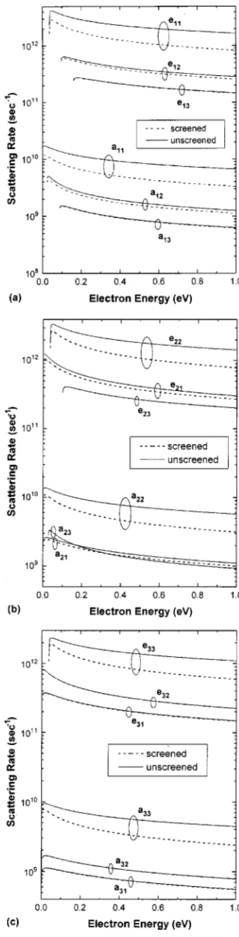
In order to see the effects of screening on POP scatter-ing, we calculated two-dimensional POP scattering rates for both screened and unscreened cases. Figure 3 shows the POP emission and absorption rates at 77 K for the pseudomor-phic Ga0.51In0.49P/In0.15Ga0.85As/GaAs structure with an In0.15Ga0.85As layer thickness of 10 nm and a Ga0.51In0.49P
FIG. 2. 2D POP scattering rates in the second subband of the Ga0.51In0.49P/GaAs structure with a barrier layer doping of 2⫻10
18cm⫺3
calculated using the exact and trial wave functions at 77 K. ei j and ai j
represent the emission and absorption rates from subband i to j, respec-tively.
FIG. 3. 2D POP scattering rates in the Ga0.51In0.49P/In0.15Ga0.85As/GaAs
structure with a barrier layer doping of 2⫻1018cm⫺3at 77 K. e
i jand ai j
represent the emission and absorption rates from subband i to j, respec-tively. InGaAs layer thickness is 10 nm. First subband共a兲, second subband
layer doping of 2⫻1018cm⫺3. The intrasubband POP scat-tering rate is significantly lowered due to dielectric screen-ing, whereas the intersubband rates are almost unaffected. This is mainly due to the rapidly decreasing strength of the intersubband Coulomb matrix elements, Hi jkl(q). Similar differences between screened and unscreened POP rates were seen in our calculations for single well modulation doped Ga0.51In0.49P/GaAs structures.
IV. EFFECTS OF SCREENING ON TRANSPORT PROPERTIES
In order to see the effects of screening on the two-dimensional electron gas transport, we calculated the trans-port properties of Ga0.51In0.49P/InxGa1⫺xAs/GaAs (x⫽0,
0.15, and 0.25兲 heterostructures by performing steady-state Monte Carlo simulations at 77 and 300 K for both screened and unscreened cases. Three valleys of the conduction band
共⌫, L, and X) and band nonparabolicities were included by
considering size quantization in the ⌫ valley and the first three subbands in the quantum well. L and X valleys were assumed to have 3D properties. We also treated the electrons with energies larger than the third subband energy as three dimensional. This assumption can be justified due to the closer spacing of the energy levels at high energies which forms a quasicontinuum as in the case of bulk material. The simulation starts by launching the electron in the two-dimensional system. The trajectory of the electron subjected to two-dimensional scattering mechanisms is followed under the applied field, and the electron is placed in the 3D system after it is scattered to the third subband or to the L and X valleys. Once the electron enters the 3D system, it is sub-jected to 3D scattering mechanisms until it is scattered back to the 2D system. A similar way of two to three dimensional coupling was used by Park and Brennan20 in their Monte Carlo simulations. However, their approach ignores the third and higher subbands, and places the electron in the 3D sys-tem after the electron’s energy exceeds the band bending energy. We observed that including the third subband in de-scribing the intersubband scattering processes yields more accurate results. In the quantum well, the scattering mecha-nisms included in the simulation are polar optical phonon scattering, acoustic phonon scattering, and intervalley
共equivalent and nonequivalent兲 scattering. Self-consistently
calculated electronic states were used in the calculation of the 2D scattering rates. We ignored the impurity scattering in the quantum well, since the channel is not considerably doped. The scattering rates for 3D electrons are the same as those given by Fawcett et al.27
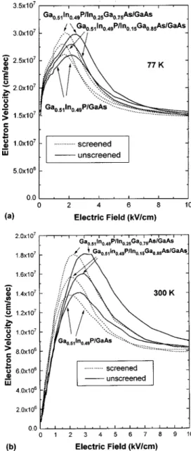
Velocity-field characteristics for Ga0.51In0.49P/
InxGa1⫺xAs/GaAs modulation doped heterostructures with
different channel In mole fractions (x) are shown in Fig. 4. The barrier layer donor doping in the structures is 2
⫻1018cm⫺3 and InGaAs layer thickness is 10 nm in the
pseudomorphic structures. The critical field is significantly shifted to lower values at both 77 and 300 K in the screened case. This shift is mainly due to the lower rate of intrasub-band scattering in the screened case which results in a lower energy relaxation rate by POP emission. Therefore, in the
screened case electrons gain energy from the field at a higher rate and are transferred to lower mobility valleys at relatively low electric fields. Under large fields the difference between the screened and unscreened cases diminishes, since most of the electrons are transferred to 3D-like bands and are sub-jected to 3D scattering mechanisms for which the screening effects are ignored.
Figure 5 presents the band populations at 77 K for the Ga0.51In0.49P/In0.15Ga0.85As/GaAs structure in the field range
of 1–5 kV/cm. While subband 1 population is lower in the screened case, screening increases the populations of other bands. The decrease in the population of subband 1 with screening is due to a more rapid transfer of electrons from subband 1 to subband 2 and to satellite valleys. The intra-subband POP scattering rates in intra-subband 2 are also decreased with screening resulting in a lower energy relaxation rate in this subband by POP emission. However, screening increases the occupancy of this band due to higher electron transfer
FIG. 4. 77 K 共a兲 and 300 K 共b兲 velocity-field characteristics of lattice matched and pseudomorphic heterostructures. InGaAs layer thickness is 10 nm in the pseudomorphic structures.
1507
rate to this subband from subband 1. The maximum 3D-⌫ band occupancy is below 20% showing that significant inter-valley transfer starts when the electron energy in the quan-tized system is large enough to populate the third subband. Therefore, taking only the lowest two subbands into account and treating the electron as a 3D electron once it is scattered to the third subband is a reasonable approach in the Monte Carlo analysis of GaAs based quantum well devices.
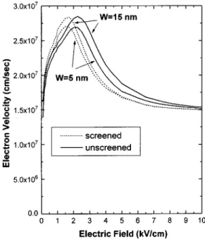
Velocity-field characteristics for Ga0.51In0.49P/
In0.15Ga0.85As/GaAs structures with two different InGaAs
layer thicknesses (W) of 5 and 15 nm are shown in Fig. 6. The structure with the 15 nm thick InGaAs layer yields bet-ter transport properties for both screened and unscreened cases, however the improvement of transport with increasing channel thickness is less apparent in the screened case. It has also been observed that screening modifies the dependence of the transport properties on the 2D electron density in the channel. The above observations clearly show that screening considerably affects the steady-state transport characteristics of the 2D electron gas in modulation doped heterostructures at both 77 and 300 K.
V. HEMT SIMULATIONS
In order to see the effects of POP screening on HEMT performance, we performed ensemble HEMT Monte Carlo simulations under both screened and unscreened conditions. The simulated device structure is shown in Fig. 7. The simu-lation is started with 5⫻104electrons distributed throughout the device based on the doping profile. In order to obtain the two-dimensional potential profile in the device, Poisson’s equation is solved calculating the total charge in each cell by the cloud in cell method.28The time interval for the solution of the equation is selected so that an electron is not allowed to drift through more than one mesh during the interval. The
charge neutrality in the source and drain contacts are pre-served by injecting new electrons or removing the excess electrons. When the steady state is reached, the number of electrons entering the device becomes equal to the number of electrons leaving the device. The electrons which hit the sur-faces are reflected and their wave vectors and positions are changed accordingly. Two to three dimensional coupling is as described in Sec. IV for steady-state transport calcula-tions. Real space transfer is taken into account in the simu-lation.
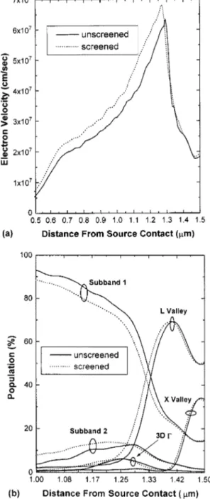
The average electron velocity in the quantum well 共av-eraged over the quantum well meshes兲 under the gate is shown in Fig. 8共a兲 for a drain-source voltage of 2 V and a gate-source voltage of ⫺1.5 V. Figure 8共b兲 shows the band occupancy in the region covering half of the gate at the drain side. Screening effects are important in both low and high
FIG. 5. 77 K band populations vs electric field in the Ga0.51In0.49P/
In0.15Ga0.85As/GaAs structure with a barrier layer doping of 2⫻10 18
cm⫺3 and InGaAs thickness of 10 nm.
FIG. 6. 77 K velocity-field characteristics for Ga0.51In0.49P/
In0.15Ga0.85As/GaAs structures with two different InGaAs layer thicknesses
(W). Barrier layer doping is 2⫻1018cm⫺3in both structures.
field regions of the device. In the screened case, the average velocity is considerably larger in a region almost completely covering the gate. In the low field regions, electrons mostly populate subband 1 and subband 2 where they are subjected to 2D scattering. Larger velocity in the screened case in low field regions is due to the larger low field mobility arising from lower intrasubband POP scattering rates. On the other hand, in the high field regions of the device near the drain side, electrons face strong electric field gradients and transfer to the L and X valleys starts. This transfer takes place slightly sooner in the screened case due to the higher energy of the electrons resulting from lower energy relaxation with POP emission. Higher peak velocity in the screened case is mainly due to the higher mobility of the electrons at the
location they face the strong field gradient near the drain side. Due to the stronger velocity overshoot in the screened case, screening effects are also important for accurate predic-tion of the high frequency performance of submicron devices through Monte Carlo simulations. The average electron ve-locities under the gate are around 3.3⫻107 and 2.9
⫻107cm/s in screened and unscreened cases, respectively.
Therefore, an error of approximately 15% is introduced in the calculation of average electron velocity along the device, if screening effects are ignored. The error introduced by ig-noring the screening effects results in a considerable under-estimation of both dc and high frequency performance of the device.
VI. CONCLUSION
The results presented above clearly show that screening is an important factor that needs to be taken into account in Monte Carlo simulations of quantum-well devices such as HEMTs. The reduction in the intrasubband POP scattering rates due to screening significantly affects the transport prop-erties of the heterostructure by decreasing the energy relax-ation rate of the two-dimensional electrons. This results in considerable error in the prediction of device performance through the simulation. Another important conclusion of this work is that screening should also be taken into account in the optimization of quantum well structures for better trans-port characteristics and device performance, since this effect may modify the dependence of transport properties on the quantum well parameters.
ACKNOWLEDGMENTS
This work is partially supported by the Scientific and Technical Research Council of Turkey under Grants No. EEEAG-168 and No. TBAG-1662, and by NATO 共SfP97 1970兲.
1C. Besikci and M. Razeghi, IEEE Trans. Electron Devices 41, 1066
共1994兲.
2
Y. J. Chan, D. Pavlidis, M. Razeghi, and F. Omnes, IEEE Trans. Electron Devices 37, 2141共1990兲.
3C. Besikci, Y. Civan, S. Ozder, O. Sen, C. Jelen, S. Slivken, and M.
Razeghi, Semicond. Sci. Technol. 12, 1472共1997兲.
4
C. Besikci and Y. Civan, Thin Solid Films 338, 213共1999兲.
5M. Takikawa, T. Ohori, M. Takechi, M. Suzuki, and J. Komeno, J. Cryst.
Growth 107, 942共1991兲.
6B. Pereiaslevats, G. H. Martin, L. F. Eastman, R. W. Yanka, J. M.
Ball-ingall, J. Braunstein, K. H. Bachem, and B. K. Ridley, IEEE Trans. Elec-tron Devices 44, 1341共1997兲.
7B. K. Ridley, J. Phys. C 15, 5899共1982兲. 8P. J. Price, Ann. Phys. 133, 217共1981兲. 9P. J. Price, Surf. Sci. 113, 199共1982兲. 10
K. Hess, Appl. Phys. Lett. 35, 484共1979兲.
11K. Yokoyama and K. Hess, Phys. Rev. B 33, 5595共1986兲. 12P. K. Basu and B. R. Nag, Appl. Phys. Lett. 43, 689共1983兲.
13M. Tomizawa, K. Yokoyama, and A. Yoshii, IEEE Electron Device Lett.
5, 464共1984兲.
14
K. S. Yoon, G. B. Stringfellow, and R. J. Huber, J. Appl. Phys. 62, 1931
共1987兲.
15K. S. Yoon, G. B. Stringfellow, and R. J. Huber, J. Appl. Phys. 63, 1126
共1988兲.
16
O. Sen, C. Besikci, and B. Tanatar, Solid-State Electron. 42, 987共1998兲.
17G. Salmer, J. Zimmerman, and R. Fauquembergue, IEEE Trans.
Micro-wave Theory Tech. 36, 1124共1988兲.
FIG. 8.共a兲 Average electron velocity in the quantum well under the gate for a drain-source voltage of 2 V and a gate-source voltage of ⫺1.5 V. The velocity is averaged over the meshes in the quantum well.共b兲 Band occu-pancy in the region covering half of the gate at the drain side.
1509
18K. Tomizawa and N. Hashizume, IEEE Trans. Electron Devices 35, 849
共1988兲.
19U. Ravaioli and D. K. Ferry, IEEE Trans. Electron Devices 33, 677
共1986兲.
20D. H. Park and K. F. Brennan, IEEE Trans. Electron Devices 36, 1254
共1989兲.
21
P. J. Price, J. Vac. Sci. Technol. 19, 599共1981兲.
22P. K. Basu and S. Kundu, Appl. Phys. Lett. 47, 264共1985兲.
23P. C. Chow, Am. J. Phys. 40, 730共1972兲.
24F. Stern and S. Das Sarma, Phys. Rev. B 30, 840共1984兲.
25P. Sotirelis, P. von Allmen, and K. Hess, Phys. Rev. B 47, 12744共1993兲. 26
S. Mori and T. Ando, Phys. Rev. B 19, 6433共1979兲.
27W. Fawcett, A. D. Boardman, and S. Swain, J. Phys. C 31, 1963共1970兲. 28R. W Hockney and J. W. Eastwood, Computer Simulation Using Particles