Content from this work may be used under the terms of theCreative Commons Attribution 3.0 licence. Any further distribution of this work must maintain attribution to the author(s) and the title of the work, journal citation and DOI.
Published under licence by IOP Publishing Ltd
Elastic, Electronic, and Optical properties of NaSnX (X=Sb,
Bi, As): First principle calculations
Husnu Koc1, Amirullah M Mamedov2,3, Ekmel Ozbay2
1Siirt University, Faculty of Science and Letters, Department of Physics, Siirt, Turkey 2Nanotechnology Research Center, Bilkent University, Bilkent, Ankara, Turkey 3Baku State University, International Scientific Center, Baku, Azerbaijan
E-mail: [email protected]
Abstract. In the present work, the structural, mechanical, electronic and optical properties of
NaSnX (X=Sb, B, As) compounds have been investigated by means of first principles calculations. The generalized gradient approximation has been used for modeling the exchange-correlation effects. It has been observed that the calculated lattice parameters are in good agreement with the experimental and theoretical lattice parameters. Bulk modulus, shear modulus, Young's modulus Poisson's ratio, sound velocities and the Debye temperatures using the calculated elastic constants for NaSnSb, NaSnBi and NaSnAs compounds have been obtained. The electronic band structure and the projected density of states corresponding to the electronic band structure have calculated.and interpreted. The obtained electronic band structure for NaSnSband NaSnBi compounds are metallic in nature, and the NaSnAs compound is also a narrow semiconductor. Based on the obtained electronic structures, we further calculated the frequency-dependent dielectric function, the energy-loss function, optical conductivity, and reflection along the x- and z- axes.
1. Introduction
The topological insulators (TI) have attracted a lot of attention since their theoretical discovery. The topological materials exhibit interesting paradoxes. The bulk and surface properties of these materials show different physical properties. The surface properties of these materials are different and they exhibit good conductive or superconducting properties. The finding of 2 and 3 dimensional TI materials and the use of these materials in different application areas have been the main target of the researchers [1-3]. The HgTe/CdTe quantum well was theoretically estimated as the first TI, and this estimate was confirmed by transport experiments. Later, the two-dimensional (2D) InAs / GaSb quantum well was theoretically discovered. Other 2D TI compounds such as the bismuth double layers and monolayer Bi4Br4, ZrTe5 and HfTe5 were discovered theoretically using first principle methods. Three-dimensional
(3D) TIs were initially estimated at Bi1-xSbx and then Bi2Se3, Bi2Te3 and Sb2Te3 compounds with larger
band gaps from this material were estimated [3-14].
We have determined that there is not much work in our literature research about these compounds that exhibit interesting physical properties. Dai et al. [3], using the DFT-GGA approach, calculated the bulk and surface electronic band structure of NaSnX (X = Sb, Bi, As) compounds and tried to explain the topological properties of these compounds. Jia et al. [2] studied NaXBi (X = Sn, Pb) compounds both experimentally and theoretically. In theoretical studies, they investigated the presence of the topological phase and Rashba effect by calculating the electronic band structures of the NaXBi (X = Sn, Pb) compounds using the DFT approach, and examined the dynamic and thermal properties of these
compounds by phonon spectra and DFT calculations. Our aim in this study is to fill this emptiness by examining the mechanical and optical properties of NaSnX (X = Sb, Bi, As) compounds which have not been studied theoretically as far as we know.
2. Method of calculation
In all of our calculations that were performed using the ab-initio total-energy and molecular-dynamics program VASP (Vienna ab-initio simulation program) [15-18] that was developed within the density functional theory (DFT) [19], the exchange-correlation energy function is treated within the a spin polarized GGA (generalized gradient approximation) by the density functional of Perdew et al. [20]. The potentials used for the GGA calculations take into account the 2p63s1 valence electrons of each
Na-, 4d105s25p2 valence electrons of each Sn-, 4d105s25p3 valence electrons of each Sb-, 5d106s26p3
valence electrons of each Bi-, and 3d104s24p3 valence electrons of each As-atoms. When including a
plane-wave basis up to a kinetic-energy cutoff equal to 12.16 Ha for NaSnSb/NaSnAs and 15.31 Ha for NaSnBi, the properties investigated in this work are well converged. The Brillouin-zone integration was performed using special k points sampled within the Monkhorst-Pack scheme [21]. We found that a mesh of 8x8x3 k points for NaSnSb, 12x12x4 k points for NaSnBi and 9x9x3 k point for NaSnAs was required to describe the structural, mechanical, electronic, and optical properties. This k-point mesh guarantees a violation of charge neutrality less than 0.008e. Such a low value is a good indicator for an adequate convergence of the calculations.
3. Result and discussion 3.1 Structural properties
NaSnX compounds crystallize in a hexagonal structure with the space group P63mc (No = 186). The
compounds have optimized using atomic positions and lattice parameters given in Ref.(3). The lattice parameters obtained as a result of the optimization are given in Table 1. The calculated lattice parameters are in good agreement with the experimental and theoretical lattice parameters given in Table 1.
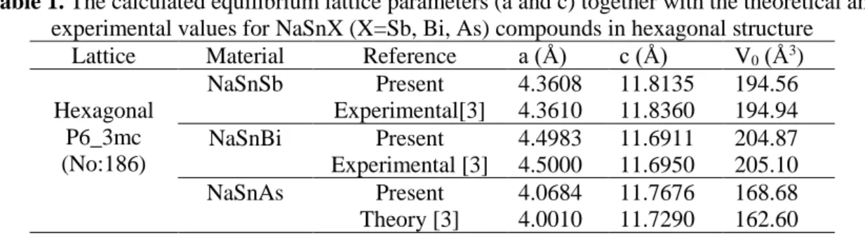
Table 1. The calculated equilibrium lattice parameters (a and c) together with the theoretical and experimental values for NaSnX (X=Sb, Bi, As) compounds in hexagonal structure
Lattice Material Reference a (Å) c (Å) V0 (Å3)
Hexagonal P6_3mc (No:186) NaSnSb Present Experimental[3] 4.3608 4.3610 11.8135 11.8360 194.56 194.94 NaSnBi Present Experimental [3] 4.4983 4.5000 11.6911 11.6950 204.87 205.10 NaSnAs Present Theory [3] 4.0684 4.0010 11.7676 11.7290 168.68 162.60 3.2. Elastic Properties
The elastic constant of a crystal is a measure of the crystalline response to the external strain applied. We used the strain-stress method [22] to calculate the elastic constants of NaSnX compounds. The obtained elastic constants are given in Table 2. The calculated elastic constants provide the mechanical stability criteria [C11>|C12|, C44>0, (C11+2C12)C33>2C132] [23,24]. The C11 and C33 elastic constants in
hexagonal crystals show resistance to linear compression in the a- and c-directions. Considering the elastic constants C11 and C33 calculated in NaSnSb and NaSnBi compounds are C11> C33 and in NaSnAs
compound is C33> C11. Therefore, NaSnSb and NaSnBi compounds are more highly compressible in the
c- direction, whereas NaSnAs is more highly compressible in the a- direction.
Table 2. The calculated elastic constants (in GPa) for NaSnX (X=Sb, Bi, As) compounds
Material Reference C11 C12 C13 C33 C44 C66
NaSnSb Present 56.17 12.68 23.45 40.69 21.75 22.85 NaSnBi Present 52.67 16.58 23.27 38.27 18.04 20.11
Using the calculated elastic constants, the bulk (B) and shear G) moduli are obtained from the Voigt (V) -Reuss (R) -Hill (H) approximation [25-27]. Young's modulus, Poisson's ratio, sound velocities, and Debye's temperature are also calculated from obtained bulk and shear moduli. The results are given in Tables 3 and 4. The value of the Poisson’s ratio is always 0.1 for covalent materials and 0.25 for ionic materials [28-30]. For this reason, the ionic character from the obtained Poisson's ratio (υ = 0.25 for NaSnSb, υ = 0.27 for NaSnBi and υ = 0.22 for NaSnAs) for all three compounds is dominant in the atomic bonding. We cannot say that these materials are stiff when we consider the value of Young's modulus (46.30 GPa, 41.16 GPa, and 27.72 GPa for NaSnSb, NaSnBi, and NaSnAs compounds, respectively), which is a measure of stiffness. if the B/G ratio is less (high) than 1.75, a material is brittle (ductile) [31,32]. Therefore, NaSnSb and NaSnAs compounds are brittle while NaSnBi compound is ductile. The calculated Debye temperature value (210.7 K) for NaSnSb is higher than the calculated Debye temperature value (172.4 K) and (176.9 K) for NaSnBi and NaSnAs. Generally, the Debye temperature is small for soft materials and large for hard materials [33-35]. We can say that all three compounds are not hard materials, but the NaSnSbcompound is harder than the NaSnBi and NaSnAs compounds.
Table 3. The calculated isotropic bulk modulus (B, in GPa), shear modulus (G, in GPa), Young’s modulus (E, in GPa), Poisson’s ratio for NaSnX (X=Sb, Bi, As) compounds
Material Reference BV BR BH GV GR GH E υ B/G
NaSnSb Present 30.24 30.16 30.20 19.72 17.48 18.60 46.30 0.25 1.62 NaSnBi Present 29.98 29.73 29.86 17.02 15.38 16.20 41.16 0.27 1.84 NaSnAs Present 16.58 16.19 16.39 11.56 11.19 11.38 27.72 0.22 1.44
Table 4. The calculated sound velocities (υt, υl, υm ) and the Debye
temperatures for NaSnX (X=Sb, Bi, As) compounds Material Reference 𝑣𝑡 (m/s) 𝑣𝑙 (m/s) 𝑣𝑚 (m/s) θD (K)
NaSnSb Present 2034 3497 2256 210.7
NaSnBi Present 1688 3008 1879 172.4
NaSnAs Present 1634 2720 1807 176.9
3.3. Electronic properties
The electronic band structures of NaSnX (X = Sb, Bi, As) compounds along the high symmetry points in the k space have calculated. The results are given in Fig. 1. As can be observed from the band structures, the NaSnSb and NaSnBi compounds are metallic but the NaSnAs compound is a narrow semiconductor with Eg = 0.04 eV. In the electronic band structure of the NaSnAs compound, the maximum of the valence band is between the Γ-K points but close to the Γ point while the minimum of the conduction band is between the Γ-M points but close to the Γ point. The results obtained for NaSnSb and NaSnBi compounds in comparison with the theoretical values [2,3] are consistent with the theoretical results, but the obtained Eg value for the narrow semiconductor NaSnAs compound is smaller than the theoretical value.
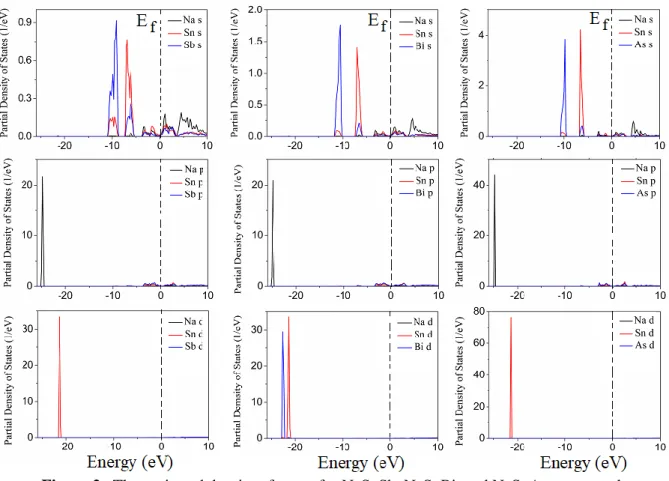
The projected density of states corresponding to the electronic band structure of all three compounds have also calculated and given in Fig. 2. In the NaSnSb compound, It is understood that the bands between -25 and -24 eV are occupied by the Na p states, and the bands between -23 and -21 eV are occupied by the Sn d states. The bands between -11 and -9 eV are occupied by the Sb s and Sn s states (but the Sb s states are more dominant than the Sn s states) while the bands between -8 and -5 eV are occupied by the Sn s and Sb s states (but the Sn s states are more dominant than the Sb s states). The bands just above and below the fermi level are occupied by all three states. In the NaSnBi compound, the lowest valence bands are occupied by Na p states. the bands between -23 and -21 eV are occupied by the Sn d and Bi d states. The bands between -11 and -9 eV are occupied by the Sb s and Sn s states (but the Bi s states are more dominant than the Sn s states) while the bands between -8 and -5 eV are occupied by the Sn s and Bi s states (but the Sn s states are more dominant than the Sb s states). The
bands just above and below the fermi level are occupied by all three states. In the NaSnAs compound, the lowest valence bands are occupied by Na p states. The bands between -23 and -21 eV are occupied by the Sn d. The bands between -11 and -9 eV are occupied by the As s and Sn s states (but the As s states are more dominant than the Sn s states) while the bands between -8 and -5 eV are occupied by the Sn s and As s states (but the Sn s states are more dominant than the Sb s states). The bands just above and below the Fermi level are occupied by all three states.
Figure 1. Energy band structures for NaSnSb, NaSnBi, and NaSnAs compounds
Figure 2. The projected density of states for NaSnSb, NaSnBi, and NaSnAs compounds 3.4. Optical properties
The optical spectra of NaSnX, which result from the band structure in Fig.1, are plotted in Fig. 3. More precisely, the real (Ɛ1) and imaginary parts (Ɛ2) of the dielectric function (Ɛ) [36,37] are displayed for
the x- and z-axis. Above ~2 eV they show more or less the same line-shape as the corresponding spectrum. The pronounced reflection peaks between ħω = 2.0 eV and 10 eV in Fig.4 still appear with almost the same intensity. However, the spectra for small photon energies ħω < 1.5 eV are totally different. The spectral weights are redistributed to guarantee the oscillator strength sum rule. An additional pronounced peak appears at ħω ≈ 10.5 eV, whereas the imaginary parts approach a small
positive value for ω → 0. Both observations are consequences of the modified band structure. The additional peak is due to van Hove singularities in the joint density of states at the highest optical transition energies near H and L points. The low-energy behavior is instead dominated by the non-conical 3D Dirac cones (Table 5). For intermediate energies the structure of the energy loss spectra in Fig. 3 is due to the details of the band structure. However, the high-energy behavior of the loss functions is also influenced by the collective plasmonic excitations of the valence electron with approximate plasma frequencies ω and corresponding valence electron densities. According to the band structure in Figs. 1 and 2, the valence electrons can be grouped into such due to Na p, s and Sn d electrons. Since only the valence s and p electrons can be nearly treated as free electrons in the formula for the plasma frequency, two peaks in the loss spectrum near 10.6 eV (only p electrons) and 13. eV (s and p electrons) can be explained. Because of the stronger binding, the right effective mass of the X p-d electrons is larger than the free-electron mass. Consequently, two other structures near 12.5 and 15.1 eV may be related to collective excitations where the delectrons partially contribute. The pronounced peak around ħω = 10.3 eV can be explained by contributions from the lowest Na s and X p bands into higher-lying conduction bands with p character.
Table 5. Some of the principal features and singularities of the linear optical responses for NaSnSb, NaSnBi and NaSnAs
Material Ɛ1(eV) dƐ1/dE<0 dƐ2/dE>0 Ɛ2(eV) L (eV)
NaSnSb ε1 x 3.02 12.71 ε 2,max x 2.42 L X 13.32 ε1z 4.84 12.71 ε2,maxz 4.24 LZ 13.31 NaSnBi ε1 x 2.76 11.06 ε 2,max x 2.07 L X 11.06 ε1z 4.15 11.75 ε2,maxz 3.46 LZ 13.82 NaSnAs ε1 x 2.82 11.87 ε 2,max x 1.77 L X 13.34 ε1z 3.67 12.85 ε2,maxz 3.06 LZ 13.34
Figure 3. The real (Ɛ1) and imaginary (Ɛ2) parts of the dielectric function (Ɛ) and energy-loss
function (L) along the x- and z- axes for a) NaSnSb, b) NaSnBi and c) NaSnAs
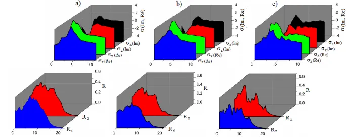
The real( σ1) and imaginary σ(2) parts of optical conductivity (σ= σ1+ iσ2) are shown in Fig. 4 for the whole investigated spectral range. In inspecting the spectra of the real part of σ first, we recognize a metallic-like contribution merging into a Drude-like resonance well below 2 eV. All other peaks above 2 eV dominate σ1 in the investigated compounds. We have proposed to ascribe all of these absorption peaks to generic electronic interband transitions. Their resonance frequencies closely coincide indeed with the direct transition along the Γ-K-L directions in the reciprocal space, as predicted by band structure calculations. The main panel of Fig. 4 emphasizes σ1 in the spectral range of relevance for the following discussion. Again, we can appreciate the narrow metallic contribution and the two of the dominant absorptions pointed out here in above. These data, supported by band structure calculations, indicate that the degeneracy at the Dirac points in NaSnX is lifted by additionality breaking the
time-reversal symmetry with a canted magnetic order of the X-atoms, resulting in the formation of Weyl nodes.
Figure 4. The real ( σ1) and imaginary σ(2) parts of optical conductivity (σ= σ1+ iσ2) and reflection (R)
along the x- and z- axes for
a) NaSnSb, b) NaSnBi and c) NaSnAs 4. ConclusionWe have performed the structural, mechanical, electronic, and optical properties of the NaSnSb, NaSnBi and NaSnAs compounds using the density functional theory. The lattice parameters obtained as a result of the optimization are in good agreement with the experimental and theoretical lattice parameters. Considering the calculated elastic constants of C11 and C33, the NaSnSb-NaSnBi and NaSnAs
compounds have a higher compressible in the c- and a-directions, respectively. From the calculated Young's modulus and Debye temperature values, it is concluded that these compounds are soft materials. The ionic character from obtained Poisson's ratio for all three compounds is dominant in the atomic bonding. The electronic band structures and the projected density of states corresponding to these band structure have been calculated. The NaSnSb and NaSnBi compounds are metallic in nature, but the NaSnAs compound is a narrow semiconductor. The real and imaginary parts of the dielectric function, energy-loss function, optical conductivity, and reflection for these compounds have been calculated and interpreted.
5. References
[1]
Hasan M Z and J. E. Moore J E 2011 Annu. Rev. Condens. Matter Phys. 2 55 https://doi.org/10.1146/annurev-conmatphys-062910-140432[2]
Jia Y Z, Ji W X, Zhang C W, Li P and Wang P J 2018 RSC Adv. 8 27995 https://doi.org/10.1039/C8RA05458D[3]
Dai X, Le C C, Wu X X, Qin S S, Lin Z P and Hu J P 2016 Chin. Phys. Lett. 12 12730
http://cpl.iphy.ac.cn/10.1088/0256-307X/33/12/127301
[4]
Bernevig B A, Hughes T L and Zhang S C 2006 Science 314 1757
https://doi.org/10.1126/science.1133734
[5]
Moore J E 2010 Nature 464 194
https://www.nature.com/articles/nature08916
[6]
Konig M, Wiedmann S, Brüne C, Roth A, Buhmann H, Molenkamp L W, Qi X L and
Zhang S C 2007 Science 318 766
https://doi.org/10.1126/science.1148047[7]
Hughes T L, Qi X L, Wang K and Zhang S C 2008 Phys. Rev. Lett. 100 236601
https://doi.org/10.1103/PhysRevLett.100.236601
[8]
Knez I, Du R R and Sullivan G 2011 Phys. Rev. Lett. 107 136603
https://doi.org/10.1103/PhysRevLett.107.136603
[9]
Spanton E M, Nowack K C, Du L J, Sullivan G, Du R R and Moler K A 2014 Phys.
[10] Murakami S 2006 Phys. Rev. Lett. 97 236805
https://doi.org/10.1103/PhysRevLett.97.236805
[11] Zhou J J, Feng W, Liu C C, Guan S and Yao Y 2014 Nano Lett. 14 4767
https://doi.org/10.1021/nl501907g
[12] Weng H, Dai X and Fang Z 2014 Phys. Rev. X 4 011002
https://doi.org/10.1103/PhysRevX.4.011002
[13] Teo J C Y, Fu L and Kane C L 2008 Phys. Rev. B 78 045426
https://doi.org/10.1103/PhysRevB.78.045426
[14] Zhang H J, Liu C X, Qi X L, Dai X, Fang Z and Zhang S C 2009 Nat. Phys. 5 438
https://www.nature.com/articles/nphys1270
[15] Kresse G and Hafner J 1993 Phys. Rev. B 47 558
https://doi.org/10.1103/PhysRevB.47.558[16] Kresse G and Furthmüller J 1996 Comput. Mater. Sci. 6 15
https://doi.org/10.1016/0927-0256(96)00008-0
[17] Kresse G and Joubert D 1999 Phys. Rev. B 59 1758
https://doi.org/10.1103/PhysRevB.59.1758
[18] Kresse G and Furthmüller J 1996 Phys. Rev. B 54 11169
https://doi.org/10.1103/PhysRevB.54.11169
[19] Hohenberg P and Kohn W 1964 Phys. Rev. 136 A1133
https://doi.org/10.1103/PhysRev.136.B864
[20] Perdew J P and Burke S 1996 Phys. Rev. Lett. 77 3865
https://doi.org/10.1103/PhysRevLett.77.3865
[21] Monkhorst H J and Pack J D 1976 Phys. Rev. B 13 5188
https://doi.org/10.1103/PhysRevB.13.5188
[22] Le Page Y and Saxe P 2001 Phys. Rev. B 63 174103
https://doi.org/10.1103/PhysRevB.63.174103
[23] Wu Z J, Zhao E J, Xiang H P, Hao X F, Liu X J, and Meng J 2007 Phys. Rev. B 76
054115
https://doi.org/10.1103/PhysRevB.76.054115[24] Watt J P and Peselnick L 1980 J. Appl. Phys. 51 1525
https://doi.org/10.1063/1.327804[25] Voight W 1928 Lehrbook der kristallphysik (Leipsig: Teubner) p 962
[26] Reuss A 1929 Z. angew. Math. Mech. 9 49
https://doi.org/10.1002/zamm.19290090104[27] Hill R 1952 Proc. Phys. Soc. London Sect A 65 349
https://doi.org/10.1088/0370-1298/65/5/307
[28] Bannikov V V, Shein I R and Ivanovskii A L 2007 Phys. Stat. Sol. (RRL) 3 89
https://doi.org/10.1002/pssr.200600116
[29] Koc H, Yildirim A, Tetik E and Deligoz E 2012 Computational Materials Science
62 235
https://doi.org/10.1016/j.commatsci.2012.05.052[30] Koc H, Mamedov A M, Deligoz E and Ozisik H 2012 Solid State Science 14 1211
https://doi.org/10.1016/j.solidstatesciences.2012.06.003
[31] Shein I R and Ivanovskii A L 2008 J. Phys. Considens. Matter. 20 415218
https://doi.org/10.1088/0953-8984/20/41/415218
[32] Pogh F 1954 Philos. Mag. 45 823
https://doi.org/10.1080/14786440808520496[33] Johnston I, Keeler G, Rollins R and Spicklemire S 1996 Solids state physics
simulations, the consortium for upper level physics software (New York: Wiley)
[34] Anderson O L 1963 J Phys Chem Solids 24 909
https://doi.org/10.1016/0022-3697(63)90067-2
[35] Schreiber E, Anderson O L and Soga N 1973 Elastic constants and their measurements
(McGraw-Hill, New York)
[36] Philipp H R and Ehrenreich H 1963 Phys. Rev. 129 1550
https://doi.org/10.1103/PhysRev.129.1550