Optically thin composite resonant absorber at
the near-infrared band: a polarization
independent and spectrally broadband
configuration
Kamil Boratay Alici,1,* Adil Burak Turhan,1 Costas M. Soukoulis,3, 4 and Ekmel Ozbay1,2,5
1Nanotechnology Research Center, Bilkent University, Bilkent, 06800 Ankara, Turkey 2Department of Physics, Bilkent University, Bilkent, 06800 Ankara, Turkey
3 Department of Physics and Astronomy and Ames Laboratory, Iowa State University, Ames, Iowa 50011, USA 4 Institute of Electronic Structure and Laser, Foundation for Research and Technology Hellas (FORTH), and
Department of Materials
Science and Technology, University of Crete, 71110 Heraklion, Greece
5Department of Electrical and Electronics Engineering, Bilkent University, Bilkent, 06800 Ankara, Turkey
Abstract: We designed, fabricated, and experimentally characterized thin
absorbers utilizing both electrical and magnetic impedance matching at the near-infrared regime. The absorbers consist of four main layers: a metal back plate, dielectric spacer, and two artificial layers. One of the artificial layers provides electrical resonance and the other one provides magnetic resonance yielding a polarization independent broadband perfect absorption. The structure response remains similar for the wide angle of incidence due to the sub-wavelength unit cell size of the constituting artificial layers. The design is useful for applications such as thermal photovoltaics, sensors, and camouflage.
©2011 Optical Society of America
OCIS codes: (300.1030) Absorption; (160.3918) Metamaterials; (040.6808) Thermal
(uncooled) IR detectors, arrays and imaging; (350.6050) Solar energy.
References and links
1. Y. Fink, J. N. Winn, S. Fan, C. Chen, J. Michel, J. D. Joannopoulos, and E. L. Thomas, “A dielectric omnidirectional reflector,” Science 282(5394), 1679–1682 (1998).
2. R. A. Shelby, D. R. Smith, and S. Schultz, “Experimental verification of a negative index of refraction,” Science
292(5514), 77–79 (2001).
3. N. Katsarakis, Th. Koschny, M. Kafesaki, E. N. Economou, E. Ozbay, and C. M. Soukoulis, “Left- and right-handed transmission peaks near the magnetic resonance frequency in composite metamaterials,” Phys. Rev. B
70(20), 201101 (2004).
4. K. Aydin, I. Bulu, and E. Ozbay, “Focusing of electromagnetic waves by a left-handed metamaterial flat lens,” Opt. Express 13(22), 8753–8759 (2005).
5. Y. Chenga, H. Yanga, Z. Chengb, and B. Xiaoc, “A planar polarization-insensitive metamaterial absorber,” Photon. Nanostructures 9(1), 8–14 (2011).
6. K. B. Alici, F. Bilotti, L. Vegni, and E. Ozbay, “Experimental verification of metamaterial based subwavelength microwave absorbers,” J. Appl. Phys. 108(8), 083113 (2010).
7. B. Wang, Th. Koschny, and C. M. Soukoulis, “Wide-angle and polarization-independent chiral metamaterial absorber,” Phys. Rev. B 80(3), 033108 (2009).
8. H. Mosallaei and K. Sarabandi, “A one-layer ultra-thin meta-surface absorber,” Antennas Propag. Soc. Int. Symp., 2005 IEEE; IEEE: Los Alamitos, CA 1B, 615–618 (2005).
9. F. Bilotti, A. Alu, N. Engheta, and L. Vegni, “Metamaterial sub-wavelength absorbers,” Proceedings of the 2005 Nanoscience and Nanotechnology Symposium - NN2005, Frascati, Italy (2005).
10. N. I. Landy, S. Sajuyigbe, J. J. Mock, D. R. Smith, and W. J. Padilla, “Perfect metamaterial absorber,” Phys. Rev. Lett. 100(20), 207402 (2008).
11. D. Yu. Shchegolkov, A. K. Azad, J. F. O’Hara, and E. I. Simakov, “Perfect subwavelength fishnet like metamaterial-based film terahertz absorbers,” Phys. Rev. B 82(20), 205117 (2010).
12. T. K. M. Diem and C. M. Soukoulis, “Wide-angle perfect absorber/thermal emitter in the terahertz regime,” Phys. Rev. B 79(3), 033101 (2009).
#147758 - $15.00 USD Received 18 May 2011; revised 1 Jul 2011; accepted 1 Jul 2011; published 11 Jul 2011
13. C. Wu, Y. Avitzour, and G. Shvets, “Ultra-thin, wide-angle perfect absorber for infrared frequencies,” Proc. SPIE, Proceedings of Metamaterials: Fundamentals and Applications, San Diego, CA, August 10–14 (2008). 14. Y. Avitzour, Y. A. Urzhumov, and G. Shvets, “Wide-angle infrared absorber based on a negative-index
plasmonic metamaterial,” Phys. Rev. B 79(4), 045131 (2009).
15. J. Hao, J. Wang, X. Liu, W. J. Padilla, L. Zhou, and M. Qiu, “High performance optical absorber based on a plasmonic metamaterial,” Appl. Phys. Lett. 96(25), 251104 (2010).
16. K. B. Alici and E. Ozbay, “Photonic metamaterial absorber designs for infrared solar-cell applications,” Proc. SPIE 7772, 77721B, 77721B-3 (2010).
17. N. Liu, M. Mesch, T. Weiss, M. Hentschel, and H. Giessen, “Infrared perfect absorber and its application as plasmonic sensor,” Nano Lett. 10(7), 2342–2348 (2010).
18. C. H. Lin, R. L. Chern, and H. Y. Lin, “Polarization-independent broad-band nearly perfect absorbers in the visible regime,” Opt. Express 19(2), 415–424 (2011).
19. CST, GmbH, CST-Microwave Studio, Darmstadt, Germany, 2009.
20. K. B. Alici, A. E. Serebryannikov, and E. Ozbay, “Photonic magnetic metamaterial basics,” Photon. Nanostructures 9(1), 15–21 (2011).
21. E. D. Palik, Handbook of optical constants of solids (Academic Press, San Diego, 1998).
22. J. Zhou, Th. Koschny, and C. M. Soukoulis, “Magnetic and electric excitations in split ring resonators,” Opt. Express 15(26), 17881–17890 (2007).
23. K. Aydin and E. Ozbay, “Capacitor-loaded split ring resonators as tunable metamaterial components,” J. Appl. Phys. 101(2), 024911 (2007).
1. Introduction
The interaction of light with artificial periodic structures depends on the unit cell geometry and composition. These artificial periodic structures, such as photonic crystals, plasmonic structures, and metamaterials provide extensive control of light. For example, perfect reflection from a dielectric surface is achieved by stacking two different dielectrics as a one-dimensional array [1]. Another example is negative refraction and focusing property of a metamaterial composed of metallic resonators and thin wires [2–4]. One of the advantages of artificial structures over natural bulk materials is their spectral scalability. The structure can be scaled to operate at any band of the electromagnetic spectrum with slight modifications.
Recently, perfect absorption was demonstrated by utilizing structures with resonant metallic unit cells at the radio frequency (RF) [5–10], far-wavelength infrared (FIR) [11], mid-wavelength infrared (MIR) [12], near-infrared (NIR) [13–17], and visible [18] regions. Each design has its unique usefulness for specific applications in terms of spectral bandwidth, electrical thickness, polarization dependence, and the incidence angle dependent response. In the present paper, we studied perfect absorber designs utilizing “U” shaped split ring resonator particles and a very thin titanium layer in order to engineer the perfect absorption at the NIR band. The present design is based on the excitation of circulating (anti-symmetric) currents by an incident electric field. It is a different type of absorption that needs to be studied in addition to previous designs. The magnetic response of the metamaterial layer is independent of the typical back reflective plane, and high absorbance is present for multiple separation lengths between the metamaterial layer and reflective plane.
The structure of the paper is as follows. In Section 2, we present the geometry of the proposed design. In Section 3, we describe the fabrication, experimental characterization, and simulation methods. In Section 4, we present the results of the experimental characterization and the simulations of the absorber in terms of the spectral response. In Section 5, we extend the design to a polarization independent case and present the field distribution and power flow. Finally, in Section 6, we demonstrate the oblique performance of the absorber.
2. Design and geometry
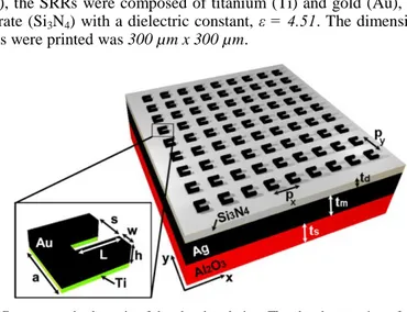
We start with a metamaterial based absorber configuration that consists of a metal back plate, a front magnetic metamaterial layer, and a dielectric layer in between. The geometry and parameters are shown in Fig. 1. The substrate, metal layer, dielectric layer, and metamaterial layer thicknesses were as follows: ts = 1 mm, tm = 300 nm, td = 115 nm, tTi = 20 nm, and h = 50 nm, respectively. The magnetic metamaterial layer consists of a two-dimensional array of magnetic inclusions, namely the split-ring resonators (SRR) as shown in the inset of Fig. 1. The parameters of the SRR were as follows: the side length of the SRR at the x and y directions were 140.7 nm < a = ax = ay < 174 nm, the periods in the x and y directions were px
#147758 - $15.00 USD Received 18 May 2011; revised 1 Jul 2011; accepted 1 Jul 2011; published 11 Jul 2011
= py = 330nm, width of the arms was 37 nm < w < 59.3 nm, separation between the arms was s = a – 2w, and the arm length was L = 104nm. The substrate was sapphire, the back metal was silver (Ag), the SRRs were composed of titanium (Ti) and gold (Au), and the dielectric was silicon nitrate (Si3N4) with a dielectric constant, ε = 4.51. The dimension of the area on which the SRRs were printed was 300 µm x 300 µm.
Fig. 1. Geometry and schematic of the absorber design. The absorber consists of an array of magnetic resonators placed on top of a thin dielectric. The wave vector (k) of the incident field is in the ̶ z-direction and the electric field (E) is in the y-direction.
3. Methodology
In the following sub-sections, we explain our nano-fabrication techniques, experimental characterization setups, and numerical simulations.
3.1 Nano-Fabrication
Firstly, we prepared the sapphire substrate on which the metallic resonators would be printed. It was diced into 10 mm x 6 mm dimensions, cleaned in acetone, isopropanol, deionized water consecutively, and dried by using a nitrogen gas gun. Then, a patterned silver layer of 300 nm thickness was coated via the electron beam evaporation method. We patterned the silver layer with photolithography: i) in order to overcome some deposition problems of silicon nitride over large areas of silver, ii) to obtain better coating quality, iii) to obtain mirror regions for calibrating the reflection response. On top of the silver back metal layer, we coated the silicon nitride dielectric layer with 130 nm thickness by using PECVD (Plasma Enhanced Chemical Vapor Deposition) equipment. We used silane, ammonia, and argon gases for this process with flow rates of 300 sccm, 10 sccm, and 50 sccm, respectively. The applied RF power was 50 W and process the pressure was 80 pA. Before pattern writing, a high resolution positive resist, which is polymethyl methacrylate (PMMA-950K-A2), was spun on the sample in order to achieve a 120 nm thickness. We baked the sample at 180°C for 90 seconds, spin-coated with aquaSAVE (sulfonated polyaniline vanish for e-beam lithography), and rebaked at 90°C for 30 seconds to prevent charging during e-beam exposure.
E-beam lithography was carried out by using Raith’s eLiNE nanolithography system. This process starts with the design of the structures that are to be exposed and continues with dose tests. In the Raith lithography software, we drew the U-shaped resonators as a composition of single pixel lines. For the dose tests, two-dimensional arrays of SRRs with slightly varying parameters were organized. A dose test exposure was performed at 7.5 kV acceleration voltage, and the sample was inserted into a developer solution of 1:3 ratio MIBK:Isopropanol and kept there for 40 seconds. The next step was metallization, and the sample was coated with gold (Au) via an e-beam evaporator machine. To promote the adhesion to the silicon nitride surface, a 20 nm layer of Ti was deposited in this evaporation process before coating the Au layer. The final steps were the lift-off and scanning electron microscopy (SEM) inspection. We determined the optimum dose for the designed dimensions. By using these
#147758 - $15.00 USD Received 18 May 2011; revised 1 Jul 2011; accepted 1 Jul 2011; published 11 Jul 2011
optimum dose test results, we fabricated the SRR array sample, as shown in the Fig. 1 background.
3.2 Experiment
The free space measurements of the samples were performed by using a homemade spectral transmission-reflection setup. The light was incident from an Ocean Optics LS-1 tungsten halogen light source. After passing through a Glan Taylor cube polarizer and a beam splitter, it focused on the two-dimensional SRR area via a Melles-Griot 20x condenser. The condenser was defined as Port 1. The beam diameter was approximately 100 µm at the focus. We collected the light with a 50x objective and sent the beam to a CCD camera by the aid of a mirror. We found the position of the absorber area by the aid of alignment marks on the sapphire sample and then centered the light beam on that area. After alignment, the light was directed toward the lens and multimode fiber. The signal was measured by using an Ocean Optics USB4000 spectrometer at the visible regime (600 nm–1000 nm) and by using a StellarNet Red Wave NIR spectrometer at the infrared regime (900 nm–1700 nm). We calibrated the sample’s transmission response with respect to bare substrate. For the reflection measurements, we used the bare metal coated sample area for calibration. The beam that was reflected from the absorber area again passed through the 20x condenser and was transmitted to another multimode fiber by way of the beam splitter.
3.3 Numerical simulations
We analyzed the magnetic metamaterial incorporated absorber unit cell by using the commercial software CST-Microwave Studio [19]. The unit cell was assumed to be infinitely periodic at the lateral directions. The frequency domain solver of the program provides the necessary unit cell boundary conditions. We used experimental data to estimate the magnetic metamaterial layer’s actual parameters such as metal loss, coated metal thickness, resonator side length, strip width, and arm length of these structures [20]. We also utilized the literature data of silver, gold, and titanium in order to model the metal parameters. Moreover, detailed SEM inspections gave us the parametric variations of the fabricated samples.
5. Results and discussions
When samples are fabricated with the e-beam lithography fabrication technique, the resonator parameters can be different from the designed ones on the order of 10 nm. We had to find a method that could take into account these fabrication imperfections in the simulations. We observed in SEM inspections that each individual SRR actually had different parameters from the others’ parameters. The parameters varied at most 5-10 nm from one SRR to another at different regions of the 2D array. The effect of different parameters on the magnetic resonance frequency was demonstrated in the literature recently [20]. This variation was taken into account by using a super-cell composed of a 6x6 array of SRRs whose parameters were varied in accordance with the SEM data. The dispersion characteristics of metals are of critical importance at the optical regime. The complex metal permittivity was tabulated in Palik [21]. We used these data to calculate the Drude model parameters of the materials. The Drude model permittivity was given by the formula: ε(ω)=ε+ωp2/ω(ω-iνc), where ωp was the plasma frequency and νc was the collision frequency. Our fit to the data of Palik implied ωp = 13250x1012 rad/s and νc = 130 THz for silver, ωp = 12000x10
12
rad/s and νc = 105 THz for gold and ωp = 14500x1012 rad/s and νc = 5500 THz for titanium.
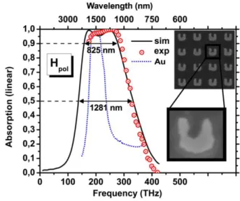
We show the simulated and measured absorption (A) derived from the scattering parameters: the magnitude of transmission (|S21|), and reflection (|S11|) in Fig. 2. We observed a reflection dip at around the magnetic resonance frequency of the SRRs and the structure behaves like a resonant absorber. The theory of this mechanism can be explained by considering a quarter-wavelength Fabry-Perot cavity [11]. When the electromagnetic field impinges on the structure from port 1, the absorbance of the structure is calculated by the formula: A = 1– |S11|
2 – |S21|
2
. We obtained a 99.3% absorbance peak at 250 THz (1200 nm). The full width at 90% absorption was around 121 THz (825 nm). The total thickness of the
#147758 - $15.00 USD Received 18 May 2011; revised 1 Jul 2011; accepted 1 Jul 2011; published 11 Jul 2011
absorber was τ = td + tTi + h = 185 nm, which corresponds to λ/6.5 at the central frequency of operation. The presence of the titanium layer is of critical importance for the broadband operation. In Fig. 2, the blue dotted line corresponds to a super-cell with gold-only SRRs. We can clearly see that the addition of a correctly tuned Ti SRR layer shifted the gold-only SRR peak to red and also broadened the bandwidth.
Fig. 2. Numerical and experimental data of absorbance derived from scattering parameters. The blue dotted line corresponds to gold-only SRR layer performance. The SEM image of a section of the printed area and an example SRR are shown on the right.
The magnetic response of the metamaterial layer is independent of the back metal and high absorbance is present for multiple dielectric spacer thicknesses that may be desired for specific applications. As we increased the dielectric layer thickness, the absorption magnitude shows an oscillatory behavior, and the maxima and minima depend on the surface impedance variation of the metamaterial layer. The minimum separation that is necessary between the metamaterial layer and the back metal for an absorption maximum was λ0/(4.9nd) at the center frequency of operation (250 THz). Here, nd is the index of the dielectric layer and λ0 is the magnetic resonance wavelength. The absorbance decreases and increases periodically as we vary the dielectric thickness. Higher order absorption maxima do not show a linear dependence on the dielectric layer thickness.
The magnetic resonance frequency of the individual SRRs strongly depend on the resonator arm length (L). By changing L, we can change the resonance frequency considerably, which is one of the reasons for the wide bandwidth response in the experiments as large parametric variations for L were present at the fabricated samples.
Up to this point, we showed that the design works for normal incidence and single polarization. In the following sections, we show a slightly different design that operates independent of incident polarization and for wide incidence angles.
6. Polarization insensitive and wide bandwidth composite structure
We added a resistive sheet (thin titanium) layer between the metamaterial and dielectric layers. The three layer configuration composed of resistive sheet, dielectric spacer, and back metal itself behaves as a resonant absorber. By changing the thickness of the titanium layer, its electrical surface impedance can be tuned. In order to obtain wide bandwidth operation, the resistive sheet resonant absorption wavelength and metamaterial layer resonant absorption wavelength can be combined. We merged the two structures and the composite absorber thereby had a larger bandwidth than the two individual cases. The thickness of the titanium
#147758 - $15.00 USD Received 18 May 2011; revised 1 Jul 2011; accepted 1 Jul 2011; published 11 Jul 2011
layer was tTi = 2 nm, SRR height was h = 40 nm, and the dielectric layer thickness was td = 110 nm in this design.
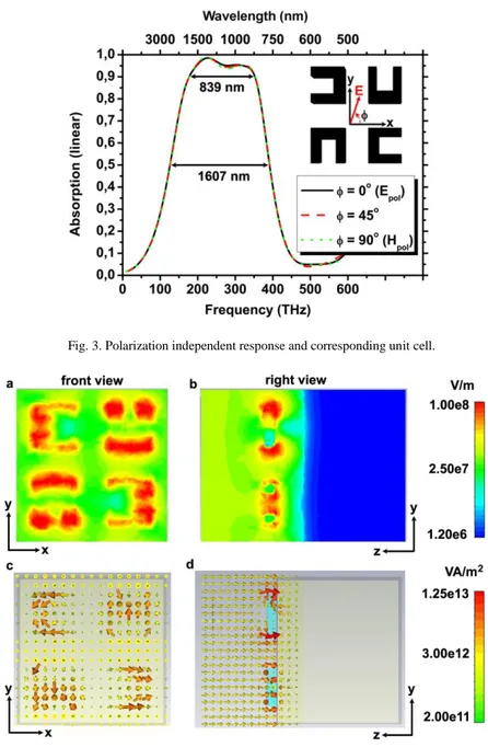
Fig. 3. Polarization independent response and corresponding unit cell.
Fig. 4. Spatial field distributions in the vicinity of split ring resonators at 225 THz frequency. (a)-(b) Electric field amplitude: (a) Top view (four unit cells were shown) (b) Side view (two unit cells were shown). (c)-(d) Spatial distribution of power flow. The color of the arrows shows the magnitude and direction of the arrows show the direction of the power flow. (c) Top view (four unit cells were shown), (d) Side view (two units cells were shown).
In order to achieve polarization independence, we changed the unit cell so that it is now composed of 4 SRRs. There are elements parallel to the y-direction and other elements that are parallel to the x-direction, as shown in Fig. 3. We saw that the simulated absorption spectra for the incident wave polarization of 45° is the same as the polarization angles 0° and 90°, which clearly proves the polarization independent response.
#147758 - $15.00 USD Received 18 May 2011; revised 1 Jul 2011; accepted 1 Jul 2011; published 11 Jul 2011
Detailed mode profile for the excitation of circulating currents (magnetic dipole mode) by the incident electric field was studied in the literature [22, 23]. We utilized the magnetic dipole mode in our designs. In Fig. 4, the E- field amplitude, and power flow at around the center frequency (225 THz) for the composite absorber were shown. We saw the localization of the incident power between the silver metal layer and split ring resonator layer. The peak power enhancement at the dielectric region was quite high. From quantitative calculations, we discovered that nearly all of the power was absorbed by the metallic parts.
7. Oblique Response
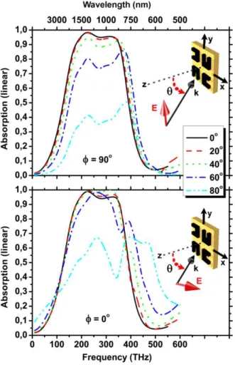
In all the data presented so far, we only characterized the absorber for normal incidence. For the oblique illumination study, we investigated the incidence angles of 20°, 40°, 60°, and 80° in the x-z and y-z planes. Figure 5 shows the spectral response for several angles of incidence: the peak absorption frequency changes and remains more than 70%, and up to a 60° angle of incidence. For oblique illumination, the excitation of SRRs is partially electrically and partially magnetically originated. The details of orientation dependent excitation have been investigated in the literature at the microwave and optical frequencies [20]. There was a slight shift of the operation frequency that slightly decreased the operation bandwidth. Even though the operation frequency of the absorber changed slightly, the absorption values remained large for up to 60° at the x-y and y-z planes.
Fig. 5. Simulated absorption response of the SRR based metamaterial absorber for several incidence angles.
#147758 - $15.00 USD Received 18 May 2011; revised 1 Jul 2011; accepted 1 Jul 2011; published 11 Jul 2011
8. Conclusions
We demonstrated metamaterial incorporated broadband absorber configurations operating at the optical regime. For a metal backed metamaterial absorber, the relation between the electrical thickness and the absorbance peak was studied. The origin of the absorbance was proven to be the magnetic resonance of the constituting artificial magnetic material inclusions. We achieved an almost full absorption with a 42% fractional bandwidth by using sub-wavelength SRRs. The total electrical thickness was approximately λ/6. The broadband absorber composed of an electrical screen in addition to the magnetic metamaterial screen and provided polarization independent and a nearly omnidirectional response. We achieved a minimum absorption of 70% for incidence angles up to 60°. These absorbers provide controllable thermal absorption and thereby controllable thermal emission. They should be useful for thermal photovoltaic, thermal sensor, and camouflage applications.
Acknowledgements
This work is supported by the European Union under the projects PHOME, and EU-ECONAM, and TUBITAK under the Project Nos. 107A004 and 107A012. One of the authors (E.O.) also acknowledges partial support from the Turkish Academy of Sciences.
#147758 - $15.00 USD Received 18 May 2011; revised 1 Jul 2011; accepted 1 Jul 2011; published 11 Jul 2011