Nonradiative recombination — critical in
choosing quantum well number for InGaN/GaN
light-emitting diodes
Yi Ping Zhang,1 Zi-Hui Zhang,1 Wei Liu,1 Swee Tiam Tan,1 Zhen Gang Ju,1 Xue Liang Zhang,1 Yun Ji,1 Lian Cheng Wang,1 Zabu Kyaw,1 Namig Hasanov,1 Bin Bin Zhu,1
Shun Peng Lu,1 Xiao Wei Sun,1,* and Hilmi Volkan Demir1,2,3,*
1Luminous! Centre of Excellence for Semiconductor Lighting and Displays, School of Electrical and Electronic
Engineering, Nanyang Technological University, 50 Nanyang Avenue, Singapore 639798, Singapore
2School of Physics and Mathematical Sciences, Nanyang Technological University, 21 Nanyang Link, Singapore
637371, Singapore
3Department of Electrical and Electronics, Department of Physics, and National Nanotechnology Research Center
Institute of Material Science and Nanotechnology, Bilkent University, Ankara TR-06800, Turkey
4[email protected] *[email protected]
Abstract: In this work, InGaN/GaN light-emitting diodes (LEDs)
possessing varied quantum well (QW) numbers were systematically investigated both numerically and experimentally. The numerical computations show that with the increased QW number, a reduced electron leakage can be achieved and hence the efficiency droop can be reduced when a constant Shockley-Read-Hall (SRH) nonradiative recombination lifetime is used for all the samples. However, the experimental results indicate that, though the efficiency droop is suppressed, the LED optical power is first improved and then degraded with the increasing QW number. The analysis of the measured external quantum efficiency (EQE) with the increasing current revealed that an increasingly dominant SRH nonradiative recombination is induced with more epitaxial QWs, which can be related to the defect generation due to the strain relaxation, especially when the effective thickness exceeds the critical thickness. These observations were further supported by the carrier lifetime measurement using a pico-second time-resolved photoluminescence (TRPL) system, which allowed for a revised numerical modeling with the different SRH lifetimes considered. This work provides useful guidelines on choosing the critical QW number when designing LED structures.
©2014 Optical Society of America
OCIS codes: (230.3670) Light-emitting diodes; (230.5590) Quantum-well, -wire and -dot
devices.
References and links
1. S. T. Tan, X. W. Sun, H. V. Demir, and S. P. DenBaars, “Advances in the LED Materials and Architectures for Energy-Saving Solid-State Lighting Toward “Lighting Revolution”,” IEEE Photonics J. 4(2), 613–619 (2012). 2. S. Pimputkar, J. S. Speck, S. P. DenBaars, and S. Nakamura, “Prospects for LED lighting,” Nat. Photonics 3(4),
180–182 (2009).
3. S. Choi, H. J. Kim, S.-S. Kim, J. Liu, J. Kim, J.-H. Ryou, R. D. Dupuis, A. M. Fischer, and F. A. Ponce, “Improvement of peak quantum efficiency and efficiency droop in III-nitride visible light-emitting diodes with an InAlN electron-blocking layer,” Appl. Phys. Lett. 96(22), 221105 (2010).
4. X. Ni, X. Li, J. Lee, S. Liu, V. Avrutin, U. Ozgur, H. Morkoc, A. Matulionis, T. Paskova, G. Mulholland, and K. R. Evans, “InGaN staircase electron injector for reduction of electron overflow in InGaN light emitting diodes,” Appl. Phys. Lett. 97(3), 031110 (2010).
5. Z. G. Ju, W. Liu, Z.-H. Zhang, S. T. Tan, Y. Ji, Z. B. Kyaw, X. L. Zhang, S. P. Lu, Y. P. Zhang, B. B. Zhu, N. Hasanov, X. W. Sun, and H. V. Demir, “Improved hole distribution in InGaN/GaN light-emitting diodes with graded thickness quantum barriers,” Appl. Phys. Lett. 102(24), 243504 (2013).
6. Y. Ji, Z.-H. Zhang, S. T. Tan, Z. G. Ju, Z. Kyaw, N. Hasanov, W. Liu, X. W. Sun, and H. V. Demir, “Enhanced hole transport in InGaN/GaN multiple quantum well light-emitting diodes with a p-type doped quantum barrier,” Opt. Lett. 38(2), 202–204 (2013).
7. Y.-J. Lee, C.-H. Chen, and C.-J. Lee, “Reduction in the Efficiency-Droop Effect of InGaN Green Light-Emitting Diodes Using Gradual Quantum Wells,” IEEE Photon. Technol. Lett. 22(20), 1506–1508 (2010).
8. S. Tanaka, Y. Zhao, I. Koslow, C. C. Pan, H. T. Chen, J. Sonoda, S. P. Denbaars, and S. Nakamura, “Droop improvement in high current range on PSS-LEDs,” Electron. Lett. 47(5), 335–336 (2011).
9. J.-Y. Chang, Y.-K. Kuo, and M.-C. Tsai, “Correlation of barrier material and quantum-well number for InGaN/(In)GaN blue light-emitting diodes,” Phys. Status Solidi A 208(3), 729–734 (2011).
10. Y.-K. Kuo, S.-H. Yen, and J.-R. Chen, “Numerical simulation of AlInGaN ultraviolet light-emitting diodes,” Proc. SPIE 6368, 636812 (2006).
11. M.-F. Huang and T.-H. Lu, “Optimization of the active-Layer structure for the deep-UV AlGaN light-emitting diodes,” IEEE J. Quantum Electron. 42(8), 820–826 (2006).
12. C. S. Xia, Z. M. Simon Li, Z. Q. Li, Y. Sheng, Z. H. Zhang, W. Lu, and L. W. Cheng, “Optimal number of quantum wells for blue InGaN/GaN light-emitting diodes,” Appl. Phys. Lett. 100(26), 263504 (2012).
13. Z.-H. Zhang, S. T. Tan, Z. G. Ju, W. Liu, Y. Ji, Z. Kyaw, Y. Dikme, X. W. Sun, and H. V. Demir, “On the Effect of Step-Doped Quantum Barriers in InGaN/GaN Light Emitting Diodes,” J. Display Technol. 9(4), 226–233 (2013).
14. Z.-H. Zhang, S. Tiam Tan, Z. Kyaw, Y. Ji, W. Liu, Z. Ju, N. Hasanov, X. Wei Sun, and H. Volkan Demir, “InGaN/GaN light-emitting diode with a polarization tunnel junction,” Appl. Phys. Lett. 102, 193508 (2013). 15. M. Meneghini, N. Trivellin, G. Meneghesso, E. Zanoni, U. Zehnder, and B. Hahn, “A combined electro-optical
method for the determination of the recombination parameters in InGaN-based light-emitting diodes,” J. Appl. Phys. 106(11), 114508 (2009).
16. M.-H. Kim, M. F. Schubert, Q. Dai, J. K. Kim, E. F. Schubert, J. Piprek, and Y. Park, “Origin of efficiency droop in GaN-based light-emitting diodes,” Appl. Phys. Lett. 91(18), 183507 (2007).
17. Q. Dai, Q. Shan, J. Cho, E. F. Schubert, M. H. Crawford, D. D. Koleske, M.-H. Kim, and Y. Park, “On the symmetry of efficiency-versus-carrier-concentration curves in GaInN/GaN light-emitting diodes and relation to droop-causing mechanisms,” Appl. Phys. Lett. 98(3), 033506 (2011).
18. J. Piprek, “Efficiency droop in nitride-based light-emitting diodes,” Phys. Status Solidi A 207(10), 2217–2225 (2010).
19. T. Wang, D. Nakagawa, J. Wang, T. Sugahara, and S. Sakai, “Photoluminescence investigation of InGaN/GaN single quantum well and multiple quantum wells,” Appl. Phys. Lett. 73(24), 3571–3573 (1998).
20. Y. Ji, W. Liu, T. Erdem, R. Chen, S. T. Tan, Z.-H. Zhang, Z. G. Ju, X. Zhang, H. Sun, X. W. Sun, Y. Zhao, S. P. DenBaars, N. Shuji, and H. V. Demir, “Comparative study of field-dependent carrier dynamics and emission kinetics of InGaN/GaN light-emitting diodes grown on (112¯2) semipolar versus (0001) polar planes,” Appl. Phys. Lett. 104(14), 143506 (2014).
21. Z.-H. Zhang, W. Liu, Z. G. Ju, S. T. Tan, Y. Ji, Z. Kyaw, X. Zhang, L. Wang, X. W. Sun, and H. V. Demir, “InGaN/GaN multiple-quantum-well light-emitting diodes with a grading InN composition suppressing the Auger recombination,” Appl. Phys. Lett. 105(3), 033506 (2014).
22. S. J. Chang, W. C. Lai, Y. K. Su, J. F. Chen, C. H. Liu, and U. H. Liaw, “InGaN-GaN multiquantum-well blue and green light-emitting diodes,” IEEE J. Sel. Top. Quant. 8(2), 278–283 (2002).
23. M. Leyer, J. Stellmach, C. Meissner, M. Pristovsek, and M. Kneissl, “The critical thickness of InGaN on (0001)GaN,” J. Cryst. Growth 310(23), 4913–4915 (2008).
24. D. Holec, P. M. F. J. Costa, M. J. Kappers, and C. J. Humphreys, “Critical thickness calculations for InGaN/GaN,” J. Cryst. Growth 303(1), 314–317 (2007).
25. J. W. Matthews and A. E. Blakeslee, “Defects in epitaxial multilayers: I. Misfit dislocations,” J. Cryst. Growth
27, 118–125 (1974).
26. Y.-L. Li, Y.-R. Huang, and Y.-H. Lai, “Investigation of Efficiency Droop Behaviors of InGaN/GaN Multiple-Quantum-Well LEDs With Various Well Thicknesses,” IEEE J. Sel. Top. Quant. 15(4), 1128–1131 (2009).
1. Introduction
Owing to the advantages of high efficiency, long lifespan, high reliability, controllable color properties and ease of digitalization, GaN-based LEDs are considered as the next generation lighting sources to replace the traditional lighting devices of incandescent and fluorescent lamps [1, 2]. However, despite these advantages and the dramatic progress being made in GaN-based LED research, development and commercialization, these LEDs still suffer from a serious efficiency droop under high current density injection, which limits the expansion of these devices in the general lighting market. Hence, tremendous efforts have been devoted to overcoming this drawback and thus to improving the LED performance. Thus far, novel structures including InAlN electron-blocking layer [3] and InGaN staircase electron injector [4], graded thickness quantum barriers [5], p-doped quantum barriers [6], and gradual InGaN QWs [7] etc, have been reported to reduce the efficiency droop.
The influence of InGaN QW number on the LED performance has previously been studied and reported. Unfortunately, the reported findings are full of discrepancy and controversial in some cases. Tanaka et al. reported that the InGaN/GaN multiple quantum well (MQW) LEDs with a large number of QWs exhibited enhanced performance and they attributed this improvement to a reduced carrier concentration in QWs and thus a reduced electron overflow [8]. Chang et al. indicated that the blue 5-QW InGaN/GaN LEDs had worse performance than the 1-QW ones under low current injection levels, while the 5-QW devices are superior to the 1-QW ones at high injection currents but commented that more convincing explanations [9] are required to better understand this phenomenon. Kuo et al. suggested that the optimized performance may be obtained when the QW number is 3 for ultraviolet AlInGaN LEDs [10]. However, the simulation results from Huang et al. indicated that the optimal QW number was one for a deep-UV AlGaN LED and the performance was worse with more QWs [11]. Meanwhile Xia et al. pointed out the output power increased with the increasing QW number and the optimal QW number is 9 according to the power conversion efficiency [12]. Despite the previous reports on the effect of QW numbers on the LED performance, no conclusive remarks can be drawn. Therefore, a systematical study with complementary theoretical simulation and experimental investigation is strongly needed to resolve the discrepancy and uncover the underlying physics. Hence, in this work, blue-emitting InGaN/GaN LEDs with varied QW numbers are grown and fabricated to experimentally investigate the underpinning physics in conjunction with theoretical modeling. The influence of QW number on the performance of LED devices is understood by systematic analysis.
2. Experiments
The blue InGaN/GaN MQW LEDs used in this work were grown on c-plane sapphire substrates using an AIXTRON close-coupled showerhead metal-organic chemical-vapor deposition (MOCVD) system. All the LED wafers consisted of a 30-nm thick low-temperature unintentionally doped GaN (u-GaN) nucleation layer, a 4-µm u-GaN layer, a 2-µm thick Si-doped n-GaN layer with a Si doping concentration of 5 × 1018 cm−3.
Subsequently, LED wafers with 3, 5, 8 and 11 pairs of InGaN/GaN MQWs were grown separately with 3-nm quantum well and 9-nm quantum barrier (QB). The indium composition of the InGaN is 12% and the emission peak wavelength of the grown samples was centered at ~438 nm. After the MQWs, all LED samples were capped with a 20-nm p-type Al0.15Ga0.85N
electron blocking layer (EBL) and a 150-nm thick p-GaN layer with an effective hole concentration of 3 × 1017 cm−3. After growth, the wafers were then fabricated into chips with
device area of 350 × 350 µm2 by a standard fabrication process.
To reveal the carrier transport and carrier recombination mechanisms of the LED samples, numerical simulations were conducted by Advanced Physical Models of Semiconductor Devices (APSYS) simulator, which self-consistently solves the Schrödinger equation, continuity equation and Poisson equation with proper boundary conditions. In the simulations, the Auger recombination coefficient was set to 1 × 1042 m6/s and 40% of the
polarization charge was assumed for crystal relaxation [13]. The Shockley-Read-Hall (SRH) lifetime here was set to a constant 43 ns for the first set of simulations as is commonly done [14, 15] and later reset to be 17, 16, 15, 4.3 ns for the 3, 5, 8, 11-QW LEDs, respectively, in the second set of simulations based on the experimentally measured carrier lifetime. The lifetime measurement was carried out by a Becker & Hickl GmbH DCS-120 confocal scanning film system, which is a complete confocal laser scanning microscope for fluorescence lifetime imaging and uses a pico-second diode laser with wavelength of 375nm as the excitation source.
3. Results and discussion
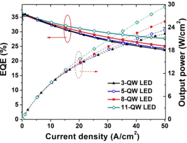
To single out how the quantum well number affects the optical power and the efficiency droop, we first performed numerical simulations on the aforementioned LED devices with the other parameters kept the same including SRH lifetime. Here, the SRH lifetime was set at 43 ns for all the LED devices. Figure 1 shows the computed EQE and output power with increasing current density for the LEDs of varying QW numbers. It is shown that, as the QW number increases from 3 to 11, both the output power and the EQE are enhanced at all current density levels and these enhancements become increasingly apparent under higher injection level. More importantly, the efficiency droop is reduced as the QW number increases, which can be clearly seen in the Fig. 1. As reported by Xia et al., the improved device performance can be attributed to the reduction of electron leakage and the suppression of the Auger recombination when more quantum wells are incorporated in the LED devices and their contribution to performance improvement is significant in high current condition [12]. This explanation is supported by the electron concentration variations with the increasing quantum well number.
Fig. 1. Computed EQE and output power as a function of current density for LEDs with varying QW numbers.
The simulated electron concentration near the p-GaN is depicted in Fig. 2 (a) for the LED devices under the current injection level of 50 A/cm2, which demonstrates that the electron
concentration in the last three quantum wells close to the p-GaN region and in the p-GaN region is reduced when the QW number increases from 3 to 11. The reduction of the electron concentration in the quantum wells leads to the suppression of the Auger recombination, and the reduction of the electron concentration in the p-doped region indicates the effective suppression of the electron leakage. These results suggest that with a large number of quantum wells, the recombination volume will increase and the electrons will spread more homogeneously and be better confined within the active region. As a result, the optical power is increased and the efficiency droop is reduced, as shown in Fig. 1. It should be noted that the hole concentration in the quantum wells near the p-GaN region is increased with the increasing quantum well number, as shown in Fig. 2(b). This is possibly due to the reduced electron leakage, which leads to the reduction of the bulk recombination between the holes and electrons in the p-GaN region and allows more holes to transport into the active region. The increase in the hole concentration in the active region also benefits the LED performance.
Fig. 2. (a) Computed electron concentration in the last three QWs and in the p-GaN region for the LED samples at the current density of 50 A/cm2, (b) computed hole concentration in the
last three QWs near the p-GaN at the current density of 50 A/cm2.
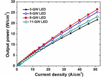
Next, the experimental optical output power from the LEDs with 3, 5, 8 and 11 pairs of QWs was measured, which is presented in Fig. 3. It shows that the output power of 3, 5, 8, and 11-QW LEDs is 21.6, 25.1, 26.5 and 23.0 W/cm2, respectively, at the current density of
50 A/cm2. The experimental output power is increased by 22.7% when the QW number
increases from 3 to 8, which is consistent with the numerical results shown in Fig. 1. However, the output power is reduced by 13.2% as the QW number further increases from 8 to 11 under the same current density, which deviates from the trend of the numerical predictions in Fig. 1.
Fig. 3. Experimental optical output power under increasing drive current density for the LEDs having 3, 5, 8 and 11 QWs.
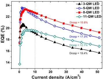
In addition, Fig. 4 shows the experimentally measured EQE versus injection current density for the LEDs with varying QW numbers. The efficiency droop is remarkably improved with the increasing QW numbers. As indicated in Fig. 4, the efficiency droop from 10 to 50 A/cm2 is 19.4%, 17.3%, 15.8% and 12.1% for LEDs with 3, 5, 8 and 11-QWs,
respectively. The trend of improvement in efficiency droop is consistent with the findings in numerical simulations. The suppression of the efficiency droop results from the reduced electron leakage [16] and the suppressed Auger recombination with the increasing QW
number, as consistently supported both by the computed and measured results. However, although 11-QW LED device shows the least efficiency droop among all in the experiments, its measured EQE is not the highest at any current density, which also deviates from the numerical predictions in Fig. 1.
Fig. 4. Experimental EQE versus injection current density for LED with varying QW numbers.
To reveal the root cause of the discrepancies between the computed and measured results, especially for the 11-QW LED device, the well-known ABC model [17] is used here for further discussions. According to the ABC model, there are three main carrier recombination mechanisms in semiconductors: Shockley-Read-Hall nonradiative recombination rate (SRH), expressed as the term An, radiative recombination rate Bn2, and Auger nonradiative
recombination rate Cn3. The IQE can be expressed as follows at low current injection level:
2/ ( 2 3) B . IQE Bn An Bn Cn A B Cn n = + + = + + (1)
The peak efficiency of IQE is achieved when ( ) 0.
d IQE
dn = (2)
Hence, the carrier concentration corresponding to the maximum efficiency is obtained at
0 /
n = A C . Here, it is worth mentioning thatn0 =J0/ev, where J0 is the current density at n0 and e is the elementary electronic charge while v is the carrier drift velocity.
Therefore, according to Fig. 4, the peak-efficiency current density J0 (the current density
at which EQE reaches the maximum) is 1.4, 1.7, 3.3 and 7.8 A/cm2 for the 3, 5, 8 and 11-QW
LEDs, respectively. It is reasonable that we assume the Auger recombination coefficient in the quantum well region is an invariant for all the grown LED devices. Thus, an increased SRH recombination coefficient is obtained for the LED devices with a large quantum well number and this is consistent with the Joachim Piprek’s finding that the maximum EQE is significantly influenced by SRH recombination [18]. Here, it is worth mentioning that the self-absorption by QW is insignificant since the QW is thin. Therefore, the increasingly serious SRH recombination is responsible for this degradation of the LED performance and it can be caused by the degradation of crystal quality [19] due to the increased thickness. The SRH recombination within the quantum wells is represented by the defect-related carrier
lifetime. It was set to a constant value of 43 ns for all the devices in the simulation shown Fig. 1, which is not proper as analysed from the experimental data here. This may cause the difference between the numerical and experimental results in Figs. 1, 3 and 4.
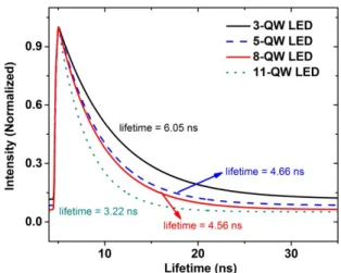
In order to experimentally support this explanation, the carrier lifetime measurement for GaN LED devices with varied QW numbers was carried out by using a pico-second TRPL system [20] and the results are presented in Fig. 5. The decay time turns out to be shorter as the QW number increases. As indicated in Fig. 5, the carrier lifetime is 6.05, 4.66, 4.56 and 3.22 ns for LEDs with 3, 5, 8 and 11 QWs, respectively. The difference among these decay times under the low excitation power is mainly attributed to the different nonradiative recombination rates, which is ascribed to the SRH recombination rate since Auger recombination rate is minor under the low excitation level [21]. Therefore, the reduced carrier lifetime of LED devices with increasing QW number can be a solid support to the claim that in the practical growth a more serious defect-related SRH recombination would be induced in LED devices with more QWs. Here, it is necessary to note that the carrier lifetime for the 11-QW LED device is much shorter compared to that for other LED devices with smaller 11-QW number, which is believed to be caused by the strain relaxation in this sample. When the effective thickness of the lattice-mismatched MQW active region is beyond its critical layer thickness [22], the misfit strain relaxation accompanied with the generation of defects takes place during the epitaxial growth. The strain relaxation is most likely to take place for the 11-QW LED device according to other reports [23–25]. Thus considerable defects generated in the relaxation process lead to the significant SRH nonradiative recombination. To further verify the above conjecture, the numerical simulations were performed again by resetting a decreased related carrier lifetime for the studied devices, that is to say, the defect-related carrier lifetime was set to 17.0, 16.0, 15.0 and 4.3 ns for the 3, 5, 8 and 11-QW LEDs, respectively. The lifetime for 11-QW LED is set much smaller to account for the effect of the formation of a large number of defects in the strain relaxation. The simulated results are presented in Fig. 6, which exhibits the same trend as the experimental results given in Fig. 4. Here, it is worth mentioning that at low current density, for example 10 A/cm2, the EQE
difference between these LED devices both in experimental and re-produced numerical results is considerable, and this is because the SRH phenomenon is dominant and has significant effect on radiation process under the low current condition. This similarity in turn supports the validity of SRH lifetime in the revised numerical calculations. It is necessary to point out that the analysis in this work is based on the low current density where the SRH recombination is dominated and is responsible for the degradation of the optical output power and EQE. When it comes to higher current density, Auger recombination and electron leakage is the dominant mechanism for efficiency droop and determines the performance [26]. Based on the trend of EQE curve and efficiency droop rate shown in Fig. 4, it is possible that the 11-QW LED device will perform best in the even higher current condition due to the alleviated electron leakage and Auger recombination.
Fig. 5. TRPL measurement for different LED devices with varied QW numbers.
The agreement between the simulated and measured results supports that the increased defect concentration appears with the increased QW number. Therefore, although increasing the QW number is an effective way to suppress the efficiency droop, the device performance enhancement is limited simultaneously by the worsening crystal quality as the QW number increases. Our findings here also clarify the discrepancy in the previous reports on the quantum well number effect, which can be due to the different crystal quality of the materials used in their works. Therefore, in order to release the full potential of an increasing number of quantum wells in reducing the efficiency droop, the growth process has to be improved in growing less-defective epitaxial films.
Fig. 6. Re-computed EQE with increasing defect concentration as a function of operation current density.
4. Conclusion
In conclusion, we found numerically that the electron leakage induced efficiency droop can be alleviated when one increases the quantum well number in the LED devices. However, experimentally we observed that the improvement in efficiency droop comes at the cost of reduced quantum efficiency when the QW number is increased beyond a certain value, which is due to the decreasing crystal quality of the epitaxial films when more quantum wells are grown. The QW number dependence of the defect-related carrier lifetime is confirmed by the carrier lifetime measurement and a good agreement has been achieved between the numerical
simulation and experimental results when the QW number dependence of the defect-related carrier lifetime is considered in the numerical simulation. Therefore, when increasing the quantum well numbers in the LEDs to reduce the electron overflow, maintaining a high crystal quality is essential to achieve the targeted level of enhanced device efficiency and reduced efficiency droop simultaneously.
Acknowledgments
We gratefully acknowledge that this work is supported by the Singapore National Research Foundation under Grant No. NRF-CRP-6-2010-2 and NRF-CRP-11-2012-01.