Frequency dependent steering with
backward leaky waves via photonic
crystal interface layer
Evrim Colak,1,* Humeyra Caglayan,1 Atilla Ozgur Cakmak,1 Alessandro Della Villa,2 Filippo Capolino,2,3 and Ekmel Ozbay1
1Department of Electrical and Electronics Engineering, Department of Physics, and Nanotechnology Research Center, Bilkent University 06800 Ankara, Turkey. 2
Department of Information Engineering, University of Siena, Via Roma 56 53100 Siena, Italy. 3Department of Electrical Engineering and Computer Science, University of California, Irvine,
CA 92697-2625, USA. *[email protected]
Abstract: A Photonic Crystal (PC) with a surface defect layer (made of
dimers) is studied in the microwave regime. The dispersion diagram is obtained with the Plane Wave Expansion Method. The dispersion diagram reveals that the dimer-layer supports a surface mode with negative slope. Two facts are noted: First, a guided (bounded) wave is present, propagating along the surface of the dimer-layer. Second, above the light line, the fast traveling mode couple to the propagating spectra and as a result a directive (narrow beam) radiation with backward characteristics is observed and measured. In this leaky mode regime, symmetrical radiation patterns with respect to the normal to the PC surface are attained. Beam steering is observed and measured in a 70° angular range when frequency ranges in the 11.88-13.69GHz interval. Thus, a PC based surface wave structure that acts as a frequency dependent leaky wave antenna is presented. Angular radiation pattern measurements are in agreement with those obtained via numerical simulations that employ the Finite Difference Time Domain Method (FDTD). Finally, the backward radiation characteristics that in turn suggest the existence of a backward leaky mode in the dimer-layer are experimentally verified using a halved dimer-layer structure.
2009 Optical Society of America
OCIS codes: (050.5298) Photonic Crystals; (240.6690) Surface Waves; (350.5500) Propagation; (350.5610) Radiation.
References and links
1. E. Yablonovitch, T. J. Gmitter, and K. M. Leung, “Photonic band structure: The face-centered-cubic case employing nonspherical atoms,” Phys. Rev. Lett. 67, 2295-2298 (1991).
2. S. John, “Strong localization of photons in certain disordered dielectric superlattices,” Phys. Rev. Lett. 58, 2486-2489 (1987).
3. E. Ozbay, E. Michel, G. Tuttle, R. Biswas, and K. M. Ho, J. Bostak and D. M. Bloom, “Double-etch geometry for millimeter-wave photonic band-gap crystals,” Appl. Phys. Lett. 65, 1617-1619 (1994). 4. B. Temelkuran and E. Ozbay, J. P. Kavanaugh, G. Tuttle, and K. M. Ho, “Resonant cavity enhanced
detectors embedded in photonic crystals,” Appl. Phys. Lett. 72, 2376-2378 (1998).
5. R. D. Meade, K. D. Brommer, A. M. Rappe, and J. D. Joannopoulos, “Electromagnetic Bloch waves at the surface of a photonic crystal,” Phys. Rev. B 44, 10961-10964 (1991).
6. P. Kramper, M. Agio, C. M. Soukoulis, A. Birner, F. Muller, R. B. Wehrspohn, U. Gosele, and V. Sandoghdar, “Highly Directional Emission from Photonic Crystal Waveguides of Subwavelength Width,” Phys. Rev. Lett. 92, 113903 (2004).
7. S. K. Morrison and Y. S. Kivshar, “Engineering of directional emission from photonic-crystal waveguides,” Appl. Phys. Lett. 86, 081110 (2005).
8. E. Moreno, F. J. Garcia-Vidal, and L. Martin-Moreno, “Enhanced transmission and beaming of light via photonic crystal surface modes,” Phys. Rev. B 69, 121402, R (2004).
9. V. D. Kumar and K. Asakawa, “Transmission and directionality control of light emission from a nanoslit in metallic film flanked by periodic gratings,” Photon. Nanostruct. Fundam. Appl. 6, 148–153 (2008).
10. H. J. Lezec, A. Degiron, E. Devaux, R. A. Linke, L. Martin-Moreno, F. J. Garcia-Vidal, and T. W. Ebbesen, “Beaming light from a subwavelength aperture,” Science 297, 820-822 (2002).
11. L. Martin-Moreno, F. J. Garcia-Vidal, H. J. Lezec, A. Degiron, and T. W. Ebbesen, “Theory of highly directional emission from a single subwavelength aperture surrounded by surface corrugations,” Phys. Rev. Lett. 90, 167401 (2003).
12. I. Bulu, H. Caglayan, and E. Ozbay, “Beaming of light and enhanced transmission via surface modes of photonic crystals,” Opt. Lett. 30, 3078-3080 (2005).
13. H. Caglayan, I. Bulu, and E. Ozbay, “Off-axis directional beaming via photonic crystal surface modes,” Appl. Phys. Lett. 92, 092114 (2008).
14. L. Wu, M. Mazilu, and T. F. Krauss, “Beam Steering in Planar-Photonic Crystals: From Superprism to Supercollimator,” IEEE J. Lightwave Technol. 21, 561-566 (2003).
15. H. Kosaka, T. Kawashima, A. Tomita, M. Notomi, T. Tamamura, T. Sato, and S. Kawakami, “Photonic crystals for micro lightwave circuits using wavelength-dependent angular beam steering,” Appl. Phys. Lett. 74, 1370-1372 (1999).
16. T. Baba and M. Nakamura, “Photonic Crystal Light Deflection Devices Using the Superprism Effect,” IEEE J. Quantum Electron. 38, 909-914 (2002).
17. A. Lai, T. Itoh, and C. Caloz, “Composite Right/Left-Handed Transmission Line Metamaterials,” IEEE Microwave Mag. 10, 34-50 (2004).
18. T. Tamir and A. A. Oliner, “Guided Complex Waves, Part I,” Proc. Inst. Electr. Eng. 110, 310 (1963). 19. T. Tamir and A. A. Oliner, “Guided Complex Waves, Part II,” Proc. Inst. Electr. Eng. 110, 325 (1963). 20. A. A. Oliner and D. R. Jackson, “Leaky-Wave Antennas,” Antenna Engineering Handbook, J. Volakis, ed.,
(McGraw Hill, (2007) Ch. 11.
21. S. Lim, C. Caloz, and T. Itoh, “Metamaterial-Based Electronically Controlled Transmission-Line Structure as a Novel Leaky-Wave Antenna with Tunable Radiation Angle and Beamwidth,” IEEE Trans. Microwave Theory Tech. 52, 2678-2689 (2004).
22. D. F. Sievenpiper, “Forward and Backward Leaky Wave Radiation With Large Effective Aperture From an Electronically Tunable Textured Surface,” IEEE Trans. Antennas and Propagat. 53, 236-247 (2005). 23. D. Sievenpiper, J. Schaffner, J. J. Lee, and S. Livingston, “A Steerable Leaky-Wave Antenna using a
Tunable Impedance Ground Plane,” IEEE Antennas Wireless Propagat. Lett. 1, 179-182 (2002). 24. L. Liu, C. Caloz, and T. ltoh, “Dominant mode leaky-wave antenna with backfire-to-endfire scanning
capability,” Electron. Lett. 38, 1414-1416 (2002).
25. T. Ueda, N. Michishita, A. Lai, and T. Itoh, “Leaky Wave Antenna Based on Evanescent-Mode Left-Handed Transmission Lines Composed of a Cut-Off Parallel-Plate Waveguide Loaded with Dielectric Resonators,” IEICE Trans. Electron. 90–C, 1770-1775 (2007).
26. I. J. Bahl and K. C. Gupta, “A Leaky Wave Antenna Using an Artificial Dielectric Medium,” IEEE Trans. Antennas and Propag. 22, 119-122 (1974).
27. D. R. Jackson, J. Chen, R. Qiang, F. Capolino, A. A. Oliner, “The Role of Leaky Plasmon Waves in the Directive Beaming of Light Through a Subwavelength Aperture,” Opt. Express 16, 21271-21281 (2008). 28. I. Bulu, H. Caglayan, and E. Ozbay, “Radiation properties of sources inside photonic crystals,” Phys. Rev. B
67, 205103 (2003).
29. I. Bulu, H. Caglayan, and E. Ozbay, “Highly directive radiation from sources embedded inside photonic crystals,” Appl. Phys. Lett. 83, 3263-3265 (2003).
30. S. Foteinopoulou, M. Kafesaki, E. N. Economou, and C. M. Soukoulis, “Backward surface waves at photonic crystals,” Phys. Rev. B 75, 245116, (2007).
31. S. Foteinopoulou, G. Kenanakis, N. Katsarakis, I. Tsiapa, M. Kafesaki, and E. N. Economou, C. M. Soukoulis, “Experimental verification of backward wave propagation at photonic crystal surfaces,” Appl. Phys. Lett. 91, 214102 (2007).
32. F. Capolino, D. R. Jackson, and D. R. Wilton, “Fundamental Properties of the Field at the Interface Between Air and a Periodic Artificial Material Excited by a Line Source,” IEEE Trans. Antennas Propagat. 53, 91–99 (2005).
33. F. Capolino, D. R. Jackson, D. R. Wilton, “Mode Excitation From Sources in Two-Dimensional EBG Waveguides Using the Array Scanning Method,” IEEE Microwaves and Wireless Comp. Lett. 15, 49-51, (2005).
34. IEEE Stand. Def. Terms Antennas, IEEE Std. 145-1993, (1993).
35. C. A. Balanis, Antenna Theory, (John Wiley & Sons, 3rd Edition, 2005) Ch. 2 and 3. 1. Introduction
Photonic Crystals (PC) [1-4] support Bloch surface waves [5]. In order to excite surface waves, a periodic surface defect layer may be placed at the exit of a PC waveguide [6-8]. These waves are analogous to Surface Plasmons (SP) that are generated on the surface of corrugated metal films [9-11]. Each corrugation on the metal slab acts as a passive element of an array antenna, excited by its neighbors, which results in directional beaming. Similarly, in the case of a PC, surface waves are diffracted by the dielectric periodic surface scatterers, that are separated by intervals that are smaller than the free space wavelength [6-8, 12, 13]. In the
aforementioned studies, however, the generation of a directional beam and its nature are investigated, rather than the steering of the directional beam. Other studies focused on the in-plane steering of the radiation angle without relying on surface waves [14-16]. Leaky wave antennas, which are basically radiative transmission lines, have been used to achieve beam steering in the endfire and backfire directions via forward and backward leaky waves [17]. An overview of the physics of leaky waves, and their role in producing narrow-beam radiation, may be found in a pair of fundamental papers published by Tamir and Oliner in 1963 [18, 19] and also in [20]. A frequency squint (i.e., the frequency dependence of the beaming angle) is typical of leaky wave radiators [20-23]. In certain leaky wave antennas the beaming angle was adjusted electronically by changing the applied control voltage [21, 22] or mechanically by tuning the resonance frequency [23] at a single operation frequency. The use of interdigital capacitors along the transmission line [21, 24], the placement of dielectric rods in a waveguide [25], or working with a two dimensional array of copper wires [26] enables frequency dependent steering. In the work by Jackson et al. [27], a leaky wave explanation has been given for the problem of a plasmon wave on a corrugated silver surface, excited by a subwavelength aperture, that produces directive beaming of light. However, a beaming device relying on surface wave physics applicable at the optical wavelengths, and that does not rely on plasmonic waves, has yet to be reported. The use of leaky surface waves on a PC which has frequency scalability property may serve this purpose.
In the present paper, we have studied the surface mode and the radiation mode of a 2 layer PC under a surface defect layer called as the “dimer-layer” (Fig. 1). Previously, in addition to studies about the radiation behavior of sources placed inside PCs [28], the mechanism of directive radiation achieved via the surface of the PC has been already investigated [29]. The surface was regarded as a system of radiating sources whose resemblance with an array antenna was also shown. Here, the dimer-layer will be shown to support a backward guided bounded mode (surface wave) as well as a backward leaky mode. For the latter case, the PC structure behaves as a leaky wave antenna. Prior to our present study, the characteristics of surface waves propagating along a dimer-layer were investigated by Foteinopoulou et al. [30, 31], and especially backward propagating waves constituted an important part of the investigation in [30]. In [31], a modified version of the Attenuated Total Reflection technique was used in order to experimentally display the backward wave propagation phenomenon. Waves radiated by an inclined horn antenna were coupled to the surface modes of the dimer-layer via a plexiglass prism. As an alternative approach, the exploitation of line sources placed inside the periodic configuration has been used to excite surface modes [32, 33]. We have adopted this latter approach in this study: a transverse monopole source is utilized to excite the surface and leaky modes in the dimer-layer. The dispersion diagram of the arrangement is obtained by employing the Rsoft Bandsolve Software which uses the Plane Wave Expansion (PWE) Method. Changes in the radiation angle of the beam as a function of frequency are confirmed experimentally. The measurement results are also supported by Finite Difference Time Domain (FDTD) Method simulations carried out with Rsoft Fullwave Software. Finally, the experiment concerning the half dimer-layer structure is used to explain the backward characteristics of the observed radiation.
2. Experiment and analysis
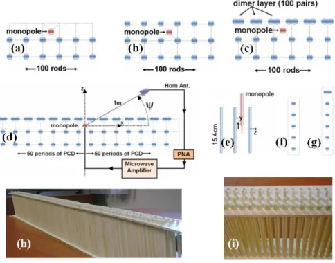
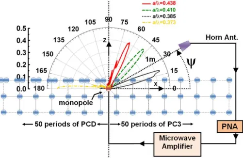
Throughout the present study, three configurations are experimentally investigated, for gaining physical insight into the formation of the narrow-angle radiation patterns: 2-Layer PC (PC2), 3-Layer PC (PC3), and 2-Layer PC with a dimer-layer (PCD), which are shown in Fig. 1. The PC and the dimer-layer are constructed with the same kind of alumina rods with a relative permittivity ε = 9.61 (refractive index n = 3.1). The rods have a diameter 2r = 3.2mm and a length of 15.4cm. The PC2 (Fig. 1(a)) is assembled as an array of 2x100 rods with a lattice spacing a = 9.6mm (r=a/6). The PC3 consists of 3x100 rods of the same kind placed with the same lattice spacing a (Fig. 1(b)). The dimer-layer placed on top of PC2 provides the PCD structure, which is the third one investigated in this work (Fig. 1(c)). Dimer rods are in contact to each other, in pairs, at the lattice corners with periodicity of a. Therefore, their
center to center distance is 2r=a/3. The monopole antenna is inserted at the mid–point, with respect to the x-direction, of the overall structure, half a lattice constant (a/2) away from the PC surface for each configuration. The monopole which has a low input reflection coefficient within the frequency band of 11-14.84 GHz (a/λ: 0.352-0.475) operates well as the excitation source. The excited transverse electric (TE) waves (along both the ±x directions) have an electric field component (Ey) parallel to the rods. As shown in Fig. 1(a), an Agilent two-port
5230A Programmable Network Analyzer (PNA) feeds the Agilent 8349B Microwave Microwave Amplifier, which drives the source antenna with a gain of 20dB. Angular distribution (AD) measurements of the transmission coefficient are carried out by employing a horn antenna as a receiver, scanning the semicircular path shown in Fig. 1(d), 1m away from the source.
Fig. 1. (a). PC2 structure, (b) PC3 structure, (c) PCD structure, (d) Experimental setup with the PCD, (e) side view of the monopole with the rods, (f) Single periodicity-cell of PC made of 5 layers (PC5), periodic along the x-direction (to be used in the simulations), (g) Single periodicity-cell consisting of the PC5 with a dimer on top, periodic along the x-direction, which is also used in the simulations, (h,i) images of the PCD that is constructed.
2.1 Dispersion diagram
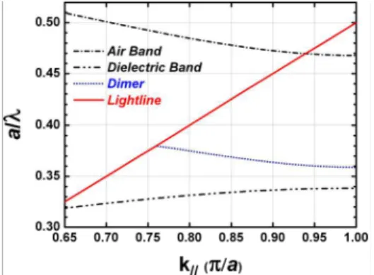
We first show in Fig. 2 the dispersion diagram of waves traveling along the x-direction for the two cases in Figs. 1(f) and 1(g), where the number of layers is the same as that considered in [30]. In particular, periodicity-cell for a PC (periodic along the x-direction) with 5 layers (PC5) stacked in the z-direction is shown in Fig. 1(f), and the structure, consisting of PC5 with a dimer-layer placed on the top is shown in Fig. 1(g). For the calculation of the band diagram, the unit cell is defined as periodic in both the z- and x-directions by the software used. The unit cell used in the simulations includes the structure shown either in Fig. 1(f) or Fig. 1(g) at the center. Besides, since we aim at simulating a structure periodic only in the x-direction, the periodicity of the unit cell along z-direction is modified as follows: Along the z-direction, 50 periods (a) of free space are left above and below the structure to be simulated (this free space region is not shown in Figs. 1(f) and 1(g)). Therefore the simulated periodic unit cell consists of a PC5 structure, with replicas separated by 100 periods (a) of empty space along the z-direction, which space is considered to be long enough to well approximate the finite number
of layers of the actual structures along z-direction. The PC5 with the dimer-layer in Fig. 1(g) is simulated in the same manner. In the dispersion diagram, obtained by using the Rsoft Bandsolve softwave, k//is the propagation wavenumber along the x-direction, and a bandgap
for 0.339<a/λ<0.468 (10.59-14.62GHz) is observed for the PC5 structure (between the dashed curves in Fig. 2). For the PC5 with dimer-layer case instead, due to the presence of the dimer layer, a defect surface mode is introduced in the dispersion diagram similar to those provided in [30, 31]. The dotted curve for the surface mode in Fig. 2 has a negative slope. The figure shows the purely real part of the propagation constant of this mode below the light line. In the measurements, we will reduce the number of PC layers while in the interpretation of the experimental work, we are still going to rely on Fig. 2 since the fields radiated by the monopole would not significantly propagate through the bottom layers of the PC, in the frequency range investigated. That is, reduction of the number of layers in PC will have a minor effect on guiding and beaming of waves created within the bandgap of the PC.
Fig. 2. Dispersion diagram describing propagation along the x-direction. The surface mode in the dimer-layer (blue dot) resides inside the bandgap bounded by the air band (dash-dot) and the dielectric band (dashed with two dots) of the PC5 structure without dimer-layer.
2.2 Radiation properties of a source embedded in the PCD
The radiation characteristics of the three configurations (PC2, PC3, and PCD) excited by the monopole are simulated by using a 2D FDTD scheme of Rsoft Fullwave software and measured using the experimental setup with the same number of rods and layers like those used in Fig. 1. Both the simulated field strength and measured transmission coefficient results are collected at a distance of 1m from the center (where the source is located). The only difference is that in the simulation the structure has been approximated as infinitely long in the y-direction, and excited by a line source.
Regarding the AD of the radiation from the monopole source which is measured in free space (i.e., without any PC), it is observed that the AD is not completely uniform in the angular range. Moreover, average value of the amplitudes in the AD decreases with increasing frequency. As a result, we have performed normalization to the measurement results with respect to source as follows: We have measured the AD of the transmission coefficient for the monopole in free space without any PC and then found the average value of the AD in the analyzed angular range (0°-180°) for each frequency. It is observed that, in the considered frequency range the variation in the average value of the AD of monopole in free space is highly correlated with the variation of the average AD of the measured transmission coefficient when the PC2, PC3 and PCD are used. Then, for the monopole which is measured in free space, we have found the least squares approximation (line fit) of the curve which represents the average value of the AD as a function of frequency. Finally for normalization, at each frequency, values of AD of the transmission coefficient measured with a PC structure is divided by the value of the line fit at the same frequency. Normalization of the measurements with respect to the measurement of the monopole in free space carried out for PC2, PC3 and PCD. Whereas, for the line source simulated in free space, variation in the
radiation is negligible in the angular and frequency range. As a result, no normalization is needed in the simulation results.
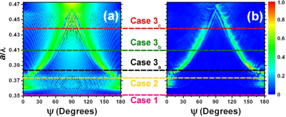
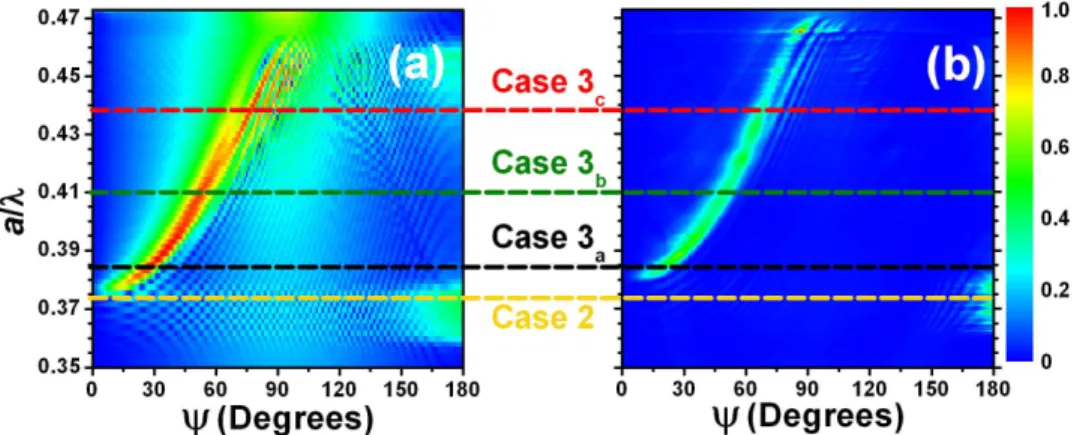
At each frequency of the simulations, the strength of the radiated signal is plotted in the Radiation Graph (RG) as a function of the observation angle (ψ) in Fig. 3(a), only for PCD. RG’s of PC2 and PC3 are not given since they are not of main interest in this work. In Fig. 3(b), the RG of the measured transmission coefficient is given. By polar-plotting a cross section at a fixed frequency (a/λ), the RG is used to extract the AD at that frequency. As a result, the values on the horizontal axis to which the peak values correspond, indicate the angular directions where the directive radiation occurs. The values in the RG are scaled such that the maximum value in the RG corresponds to 1 in both the simulations and the measurements to provide convenience in the radiation pattern comparison.
Fig. 3. RG for the PCD obtained by FDTD simulation of the field strength (a), and by measurement of the transmission coefficient (b). Dashed lines represent the sample frequencies further investigated (magenta for Case 1, yellow for Case 2, black, green, and red for Cases3a,b,c, respectively). For each case, a polar plot of the radiation pattern is provided. Comparing Fig. 3(a) to Fig 3(b), the discrepancies (i.e., non-symmetric appearance especially at high frequencies) in the measurement RG are attributed to the artifacts of the manufactured PCD and to the non ideal amplitude and frequency (i.e., non-uniform AD) characteristics of the monopole source.
Three different cases will be of interest for us, whose distinction is made in terms of frequency ranges, based on what is observed in the dispersion diagram (Fig. 2) and in the RG of PCD (Fig. 3).
Case 1: The frequency range 0.339<a/λ<0.359 (10.59-11.22GHz) starts from the lower
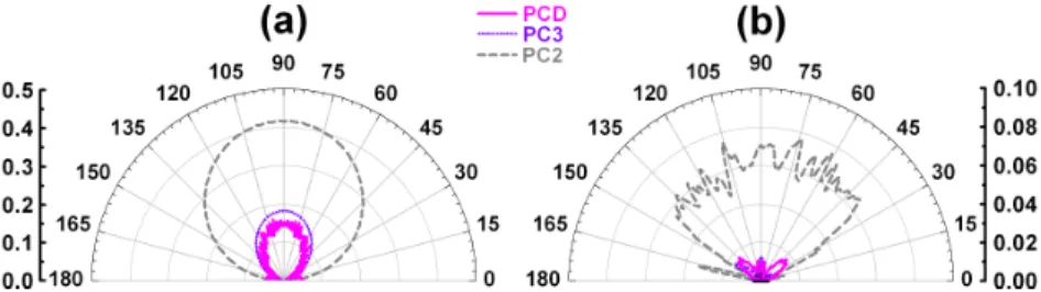
band edge and extends up to the lower-frequency tail of the dimer-layer mode shown in Fig. 2. These frequencies reside in the PC and PCD stopband and do not couple to the dimer-layer mode unless the frequency is too close to the minimum frequency of the dimer-layer mode. The AD plots of radiated field for the three configurations (PC2, PC3, and PCD) are drawn in Fig. 4 at the frequency a/λ=0.353. Although, for PCD, Fig. 3 predicts no significant radiation for any angle at this frequency, Fig. 4 is given in order to make a fair and consistent comparison between the investigated structures. Irregularities in the measurement results arise from the low power radiation levels. In all of the three configurations, radiation around ψ=90o is observed because either there are no rods in front of the source to prevent radiation (for PC2) or because of the poor filtering capability of a single layer of dielectric rods that is placed in front of the source (for PC3 and PCD). In Case 1, surface states are not excited so that propagation along the layer is negligible unless the frequency is close to the dimer-layer mode frequencies. Figure 4(a) shows that at a/λ=0.353 a small radiation in the region ψ=0° and ψ=180° occurs for the PCD. This results from the minor surface propagation due to the weak excitation of the mode represented by the lower-frequency tail of the dimer-layer mode starting at a/λ=0.359 (Fig. 2). Moreover, in the PCD case the same minor surface propagation is the reason for the high frequency oscillations shown in Fig. 4(a). This issue is going to be clearer after the discussion of surface modes and surface propagation in Case 2.
These oscillations can not be recognized in the radiation pattern obtained by measurement given in Fig. 4(b), due to the very low signal strength.
Fig. 4. Normalized angular field distribution for Case 1 at a/λ=0.353. (a) Simulation results obtained from the RG in Fig. 3(a) (b) Measurement results obtained from the RG in Fig. 3(b).
Case 2 (the guided mode): The field excited by the source couples to the dimer-layer
mode of the PCD, in the frequency region 0.359<a/λ<0.380 (11.22-11.88GHz). Below the light line (Fig. 2), the parallel wavenumber of the surface modes k// along the x-direction,
parallel to the surface of the dimer-layer, is larger than the free space wavenumber k0. In this
case, wave propagation along the dimer-layer is allowed and the power is propagating at grazing angle (ψ=0o and ψ=180o) since in this case k0 ≈ k// (but still k// >k0), without
significant radiation occurring off the dimer-layer surface. In this case, power is emitted also by the truncation-ends of the structure toward the ±x directions. Indeed, at an operation frequency of a/λ=0.373 (indicated by the yellow dashed line in Fig. 3(b)), the radiation main lobes are close to ψ=0° and ψ=180° (Fig. 5). Observation of the measured and simulated results implies the existence of guided waves along the surface due to surface mode which was observed in Fig. 2.
The oscillatory appearance in the radiation pattern is caused by the interference of the significant power coming out of the two edge-truncations because of the finite length (along
x) of the PCD. In other words, the two ends of the PCD, excited by the left and right traveling modes produced by the source, act like distinct radiating sources in addition to the direct source-field arising from the center. This situation was mentioned in discussion of Case 1 regarding the oscillations and lobes at grazing angle in the AD of PCD seen in Fig. 4(a). Since the operation frequency is still in the PC stop band, the angular field distributions relative to PC2 and PC3 do not exhibit any beaming produced by excitation of modes, which has been also similarly shown for Case 1.
Case 3 (the leaky mode): Frequencies higher than a/λ=0.380 (11.88GHz) are the main
focus of this study. At this frequency, the dimer mode crosses the light line (Fig. 2). Under this case, we make two propositions regarding the modes: P1) The wavenumber k// possesses
an imaginary part (i.e., k// is not purely real) when the real part of k// < k0 (the region above the
light line), as implied by the leaky wave theory [20]. P2) The curve representing the real part
Fig. 5. Normalized angular field distribution for Case 2 at a/λ=0.373. (a). Simulation results obtained from the RG in Fig. 3(a). (b) Measurement results obtained from the RG in Fig. 3(b).
of the propagation constant of the mode in the dimer-layer still has negative slope above the light line. Hence, the mode has a negative group velocity (vg= dω/dk < 0). A complex mode
analysis will be carried out in a future study. Nevertheless, the following observations establish a strong base for our propositions concerning Case 3. Beyond a/λ=0.380, above the light line, k// (we should say the real part of k//) is smaller than k0. The complex part of k// is
responsible for the radiation into the space above, on the right and left hand side of the PCD. Consequently, it is possible to attain two directive beams, at angles equal to ψ and (180°−ψ), as shown in Fig. 6. Since k// is decreasing when frequency increases, as a result of the
situation mentioned in P2, the radiation angle approaches broadside, ψ = 90°, as the frequency increases beyond a/λ=0.380. This behavior can be observed in Fig. 3 and Fig. 6. The PCD structure transfers power into the space above in small increments contributed discretely from each dimer and the PCD behaves like a leaky wave antenna [34]. The evanescent wave (we recall that k// has a complex value) attenuates while propagating toward the two lateral
truncation-ends of the PCD. Since most of the surface power is radiated (leaked) into the space above, only a small portion reaches the two truncation-ends of the PCD. Therefore, the oscillations in the radiation pattern that were caused by the radiation of the two truncation-ends of PCD in Case 2 are now not present. In Fig. 6(a), the far field radiation patterns are simulated by employing the far field option of the Rsoft Fullwave software. The measurement results (Fig. 6(b)) obtained at a distance of 1m are compared to the far field simulation results. The radiation patterns tend to smooth out in the far field. Moreover, the far field patterns turn out to have narrower angular beamwidths. Nonetheless, measurements performed at a distance of 1m are sufficient to offer estimates of the far field antenna behavior. The far field condition (measurement distance > 2d2/λ) given in [35] suggests the measurements being carried out at a distance of at least 20m to obtain the approximate far field distribution. Here d=0.5m is the effective aperture of the antenna and λ=2.34cm is the wavelength corresponding to a/ λ=0.41 which is an average value in the operation range. As a note, although the length of the PCD approximates 1m, the length of the effective aperture of the PCD which is responsible for the directive beam in a single quadrant covers only 0.5m, which is the length of the half section of the PCD structure. This issue will be clear when the PC with halved dimer-layer is studied in Section 2.3. The fact that for increasing frequency the beam scans toward the broadside direction (ψ = 90°) indicates that the leaky wave responsible for the directive radiation has a backward nature [20]. This is confirmed by the next experimental setup.
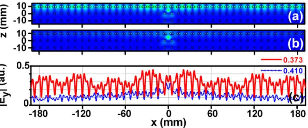
Calculated mode profiles of the electric field |Ey| in the XZ plane are shown in Fig. 7 (with
linear scale in arbitrary units) for the same input level of line source at two different frequencies. The excitation source is located between the dimer-layer and PC2, as depicted in Fig. 1(a), and here recognized by the strong field intensity at x=0mm, z=5mm. The mode profile in Fig. 7(a) confirms the presence of surface propagation at a/λ=0.373 that we have described in Case 2. Since there is not significant attenuation while propagating along the x-direction, most of the power reaches the two PCD truncation-ends. On the other hand, in Fig. 7(b), at a/λ=0.41 the guided (leaky) wave is attenuated while it propagates along the x-direction (we recall that in this case the real part of k// is smaller than k0), and only a very
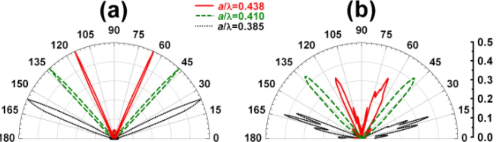
Fig. 6. Angular field distribution for Case 3abc (shown in Fig. 3) at frequencies a/λ=0.385 (black dotted line for Case 3a), a/λ=0.410 (green dashed line for Case 3b), and a/λ=0.438 (red solid line for Case 3). (a) Simulation results for the “far field” radiation pattern which are performed by Rsoft Fullwave software (previously, the simulation RG evaluated at 1m from the center was given in Fig. 3(a)). (b) Measurement results from the RG in Fig. 3(b). This shows that measurements performed at 1m provide an estimate of the far field radiation pattern.
small amount of power reaches the two PCD truncation-ends. Because of their attenuation properties, leaky waves are not permitted to cover long distances, which shows the appropriateness of P1 in Case 3. In Fig. 7(c), the cross sections of the mode profiles are given, which are taken along x-direction passing through the center of the dimers to provide a quantitative comparison. It is seen that for a/λ=0.373, energy is transferred towards the ends whereas for a/λ=0.410 the signal is decreasing along the x-direction since energy is radiated into space above the dimer layer.
Fig. 7. Calculated mode field profile for Case 2 and Case 3. (a) Case 2: the surface wave (guided) frequency is a/λ=0.373, (b) Case 3: the radiative (leaky wave) frequency is a/λ=0.41. (c) Cross sections of the mode profiles of Figs. 7(a) and 7(b), taken along x-direction passing through the center of the dimers are plotted in the same arbitrary units which is used in Fig. 3(a), Fig. 4(a) and Fig 5(a).
2.3 Backward wave character and radiation property of the leaky mode excited in the dimer-layer
We have already mentioned in our second proposition (P2) that Case 3 supports backward waves (with phase and group velocity traveling along opposite directions). This means that the radiative phenomena exhibit an interesting property. That is, the guided leaky wave with a negative phase velocity in the – (+) x direction (and positive group velocity, since power is emanated by the source in both the ± x directions) is responsible for the directional beaming in the 1st (2nd) quadrant of the polar plot. The dimer pairs on the left (right) hand side of the XZ plane act like elements of an array antenna and the cumulative interference provides the directive beaming in the range of 0°< ψ < ~70° for the 1st (180° > (180°-ψ) > ~110° in the 2nd) quadrant. This situation is typical of backward leaky wave radiation [20] and it has been used in several metamaterial-based leaky wave antennas operating in the microwave range [25]. The halved dimer-layer configuration in Fig. 8 is used to demonstrate backward nature of the
Fig. 8. The experimental setup for PCHD and the normalized AD measurement. The angular field distribution is measured at a distance of 1m at frequencies of a/λ=0.373 (yellow dash-dotted line) which is the guiding frequency, and at the beaming frequencies which are a/λ=0.385 (black dotted line), a/λ=0.410 (green dashed line), a/λ=0.438 (red solid line).
field propagating along the ± x directions, and to clearly show this we analyze the radiation by a halved dimer-layer configuration shown in Fig. 8.
The PC with a halved dimer-layer (PCHD) is very similar to the PCD except for the fact that dimer pairs for x > 0 are replaced by single rods. Therefore, the new configuration is the same with PC3 for x > 0. Surface and leaky waves are able to propagate only towards the –x direction while PC3 will not allow propagation in the +x direction. The experimental setup and the measured radiation patterns for a surface mode frequency (belonging to Case 2) and three separate frequencies (belonging to Case 3) are depicted together in Fig. 8.
The corresponding RG for the PCHD is shown in Fig. 9. As it was stated for the PCD, no radiation is observed for 0.294<a/λ<0.359. Accordingly, in the range 0.359<a/λ<0.380 the dimer-layer supports the surface mode. As a result, for a/λ=0.373, the radiation is observed only at ψ = 180° whereas no significant field is measured near ψ=0° or other angular directions. This is consistent with our earlier claims concerning Case 2. Maximum values of the RG’s in Fig. 9 are normalized to 1, for comparison.
Finally, above the light line, at higher frequencies, we observe radiation only in the 1st quadrant while the leaky wave propagation takes place in –x direction. We notice that as the frequency is increased, the radiation angle gets closer to 90° (broadside), which is the opposite of what happens to leaky wave working in the forward regime. These observations demonstrate the backward characteristics (i.e., opposite signs of phase and group velocities) of the radiation from the dimer-layer. They also confirm our prior understanding regarding the radiation phenomena for Case 3. It is also revealed that the effective aperture of PCHD (and PCD) is 0.5m (i.e., length of the dimer layer remaining at either side of the source) although the length of both structures is almost 1m.
3. Conclusion
By using a dielectric surface interface layer on top of a photonic crystal (PC), guiding of surface waves and frequency dependent beaming with leaky waves is attained in the microwave regime. Since propagation at optical frequencies is subject to significant losses in
Fig. 9. Radiation Graph for the Photonic Crystal with a halved dimer-layer. (a) Simulation of the field strength, (b) Experimental result for the transmission coefficient (yellow for Case 2, black, green, and red for Case 3a,b,c). The cross sections that are indicated by black, green, and red and yellow dashed lines are plotted in Fig. 8.
the case of the metallic surface plasmons, dielectric PC may provide an alternative to obtain surface waves. Therefore, a dimer surface layer is utilized to support surface modes (i.e., guided modes confined in the top layer) on a PC for frequencies such that the propagation wavenumber lies below the light line. The results obtained by Rsoft Bandsolve Software which employs the Plane Wave Expansion method reveal the existence of the dimer-layer mode with a negative slope in the dispersion diagram implying the occurrence of phase and group velocities with opposite directions. Above the light line, this mode couples to the radiative spectrum. As a result, the photonic crystal with a dimer-layer (PCD) provides a symmetrical and directive radiation pattern with two radiation peaks at ψ and (180°−ψ). The beaming angle ψ is adjustable as a function of frequency. In this manner, the PCD operates like a leaky wave antenna where each dimer contributes discretely to the radiated power. Although the experiments are carried out in the microwave regime, dielectric PC based structures offer scalability to optical frequencies. Angular distribution measurements are performed at a distance of 1m away from the source which is not far enough to satisfy the far field radiation condition. There is still a traceable correspondence between frequencies 0.38<
a/λ < 0.44 (11.88-13.75GHz) and measured radiation angles 0°< ψ < ~70° (simultaneously creating a symmetric beam in the 2nd quadrant at an angle 180°−ψ). At a larger measurement distance, in the far field, the symmetrical beaming angle is expected to extend beyond 70°, varying from 0° upto 90°. Another important aspect is that waves propagating along the dimer-layer cause radiation of backward nature. We have assumed two propositions to relate this backward nature to the behavior of the part of the dispersion diagram, relative to the propagating mode, which would reside above the light line (we could determine only real propagation wavenumbers, below the light line): 1) Above the light line the surface mode has an imaginary part and it is responsible for the leaky behavior, 2) The slope of the (real part) of the propagation constant above the light line is still negative (i.e., implying negative group velocity). As a result, the radiation beam angle approaches from backfire to broadside when frequency increases (this is typical of backward leaky wave antennas used in the microwave regime). Experiments and simulations relative to the halved dimer-layer are then used to demonstrate the mentioned backward characteristics and to verify the above propositions. FDTD simulations performed by Rsoft Fullwave Software have accompanied experimental measurements, and they are in good agreement, to conclusively support our propositions.
Acknowledgments
This work is supported by the European Union under the projects PHOME, and EU-ECONAM, and TUBITAK under Project Numbers 105A005, 106E198, and 107A004. One of the authors (E.O.) also acknowledges partial support from the Turkish Academy of Sciences.