SILICON NANOWIRE-BASED COMPLEX
STRUCTURES: A LARGE-SCALE
ATOMISTIC ELECTRONIC STRUCTURE
AND BALLISTIC TRANSPORT
a dissertation submitted to
the department of physics
and the Graduate School of engineering and science
of bilkent university
in partial fulfillment of the requirements
for the degree of
doctor of philosophy
By
¨
Umit Kele¸s
August, 2014
I certify that I have read this thesis and that in my opinion it is fully adequate, in scope and in quality, as a dissertation for the degree of Doctor of Philosophy.
Assoc. Prof. Dr. Ceyhun Bulutay (Supervisor)
I certify that I have read this thesis and that in my opinion it is fully adequate, in scope and in quality, as a dissertation for the degree of Doctor of Philosophy.
Prof. Dr. Ra¸sit Turan
I certify that I have read this thesis and that in my opinion it is fully adequate, in scope and in quality, as a dissertation for the degree of Doctor of Philosophy.
I certify that I have read this thesis and that in my opinion it is fully adequate, in scope and in quality, as a dissertation for the degree of Doctor of Philosophy.
Assoc. Prof. Dr. Hande Toffoli
I certify that I have read this thesis and that in my opinion it is fully adequate, in scope and in quality, as a dissertation for the degree of Doctor of Philosophy.
Assoc. Prof. Dr. Hˆaldun Sevin¸cli
Approved for the Graduate School of Engineering and Science:
Prof. Dr. Levent Onural Director of the Graduate School
ABSTRACT
SILICON NANOWIRE-BASED COMPLEX
STRUCTURES: A LARGE-SCALE ATOMISTIC
ELECTRONIC STRUCTURE AND BALLISTIC
TRANSPORT
¨
Umit Kele¸s PhD in Physics
Supervisor: Assoc. Prof. Dr. Ceyhun Bulutay August, 2014
While the hierarchical assembling as well as the dramatic miniaturization of Si nanowires (NWs) are on-going, an understanding of the underlying physics is of great importance to enable custom design of nanostructures tailored to specific functionalities. This work presents a large-scale atomistic insight into the elec-tronic properties of NW-based complex structures, starting from the subsystem level up to the full assembly, within the framework of pseudopotential-based lin-ear combination of bulk bands method. Laying the groundwork by grasping single Si NWs, we get into a large extent an unexplored territory of NW networks and kinked NWs. As one end product, a versatile estimator is introduced for the band gap and band-edge lineups of multiply-crossing Si NWs that is valid for various diameters, number of crossings, and NW alignments. Aiming for an exploration of the low-lying energy landscape, real space wave function analysis is undertaken for tens of states around band edges which reveal underlying features for a variety of crossings. Predominantly, the valence states spread throughout the network, in contrast the conduction minima are largely localized at the crossings. Given the fact that substantial portion of the band edge shift drives from the confined conduction states, branched Si NWs and nanocrystals have quite close band gap values as the networks of similar wire diameters. Further support to wave func-tion analysis is provided via quantum ballistic transport calculafunc-tions employing the Kubo-Greenwood formalism. The intriguing localization behaviors are identi-fied, springing mainly at the crossings and kinks of NWs. The ballistic transport edge set apart the conducting extended states from the localized-band gap deter-mining ones. Our findings put forward useful information to realize functionality encoded synthesis of NW-based complex structures, both in the bottom-up and top-down fabrication paradigms.
v
Keywords: Silicon nanowire, nanowire networks, kinked nanowires, electronic
structure, band edge alignments, linear combination of bulk bands, quantum ballistic transport, Kubo-Greenwood formula.
¨
OZET
S˙IL˙ISYUM NANOTEL TABANLI KARMAS
¸IK
YAPILAR: B ¨
UY ¨
UK ¨
OLC
¸ EKL˙I ATOM˙IK ELEKTRON˙IK
YAPI VE BAL˙IST˙IK TAS
¸INIM
¨
Umit Kele¸s Fizik, Doktora
Tez Y¨oneticisi: Do¸c. Dr. Ceyhun Bulutay A˘gustos, 2014
Silisyum nanoteller ve bu nanotelleri temel alarak geli¸stirilen daha karma¸sık yapılar, yeni ku¸sak nano-aygıtlarda esas yapıta¸sları olarak kullanılmaya ba¸slanmı¸stır. Ancak uygulamadaki ilerleyi¸sinin hızına kar¸sılık, nanotel temelli karma¸sık yapıların kuramsal fizi˘gi pek de incelenmemi¸stir. Oysaki bilhassa elek-triksel ve ta¸sınım ¨ozelliklerinin kavranması hem kuramsal ba˘glamda kuantum etkilerin k¨u¸c¨uk boyutlardaki tipik davranı¸slarına ı¸sık tutacak hem de uygu-lama alanında ileride yapılacak yeni aygıtların olası davranı¸sları ve sınırları i¸cin ¨ong¨or¨u olu¸sturabilecektir. Buradan hareketle, ¸calı¸smamızda tekil nan-otellerden ba¸slayarak; nanotel kav¸sakları, tel a˘gları ve dirsekli teller a¸samalı olarak irdelenmi¸stir. Oncelikle adı ge¸cen b¨¨ uy¨uk ¨ol¸cekli nano-sistemlerin elek-tronik yapıları ve bu kapsamda bant aralıkları ile bant kenarı hizalanmaları, atomik g¨or¨un¨urpotansiyel temelli yı˘gın bantların do˘grusal birle¸stirimi y¨ontemi ile ¸cıkarılmı¸stır. ˙Incelenen malzemelerin boyutu k¨u¸c¨ul¨urken, iletim bant ke-narı de˘geri, de˘gerlik bant kenarına g¨ore daha fazla de˘gi¸smektedir. Elde edilen sonu¸clar ı¸sı˘gında, ikili ve ¨u¸cl¨u kav¸saklar i¸cin farklı ¸cap de˘gerlerine g¨ore en-erji aralı˘gı ve bant hizalanmalarının ¨ong¨or¨ulmesini sa˘glayacak genel bir uyum fonksiyonu ortaya konulmu¸stur. Devamında, nanoyapıların dalga fonksiyonlarının kareleri ¨uzerinden y¨uk yo˘gunlukları ve y¨uk yo˘gunluklarının karma¸sık nanotel yapılardaki yerelle¸smeleri incelenmi¸stir. Genellikle d¨u¸s¨uk enerjili iletim durum-ları kav¸sak ve dirsek b¨olgelerinde yerelle¸sirken, de˘gerlik durumları nanoyapının geneline yayılma ¨ozelli˘gi g¨ostermektedir. Bu g¨ozlem, bant aralı˘gının daha ziyade iletim kenarının kaymasıyla olu¸stu˘gu sonucuyla birle¸stirildi˘ginde nanotel a˘gları i¸cin buldu˘gumuz sonu¸cların aynı ¸caplı dallanmı¸s nanokristal ve nanoteller i¸cin de ge¸cerli oldu˘gu g¨ozlemlenmi¸stir. Y¨uk yerelle¸smelerinin fiziksel etkilerini daha fazla
vii
kavrayabilmek i¸cin elektriksel iletim hesaplamaları yapılmı¸stır. ˙Iletim bant ke-narı, yerelle¸smi¸s enerji durumları ile malzeme boyunca iletime a¸cık olan yayılmı¸s durumları birbirinden ayırmaktadır. Yerelle¸smi¸s enerji durumları, kesi¸sen ve dirsekli nanotellerin enerji bant aralı˘gını belirledi˘gi halde iletim daha y¨uksek enerji de˘gerlerinde ba¸slamaktadır. Bulgularımız kuantum sınırlama etkisinin karma¸sık nanotel temelli yapılarda oynadı˘gı ¨onemli rol¨u ortaya koymu¸s ve ayrıca bu malzemelerin uygulamaları i¸cin faydalı ¨ong¨or¨uler sa˘glamı¸stır.
Anahtar s¨ozc¨ukler : Silisyum nanotel, nanotel a˘gları, dirsekli nanotel, balistik elektriksel iletkenlik, elektronik yapı hesabı, yı˘gın bantların do˘grusal birle¸simi, g¨or¨un¨urpotansiyel y¨ontemi, bant kenarı hizalanması, Kubo-Greenwood g¨osterimi, kuantum sınırlama etkisi.
Acknowledgement
I would like to express my deepest gratitude to my supervisor Assoc. Prof. Dr. Ceyhun Bulutay for his continuous mentoring with his endless personal and academic guidance and concern during my Bilkent years.
I acknowledgement with much appreciation the generosity of the dissertation committee: Prof. Ra¸sit Turan, Prof. O˘guz G¨ulseren, Assoc. Prof. Hande Toffoli, and Assoc. Prof. Hˆaldun Sevin¸cli for having accepted to read and evaluate my dissertation with invaluable critiques and suggestions.
This work was partially supported by T ¨UB˙ITAK with Project No. 109R037. I also acknowledge Helmholtz-Zentrum Dresden-Rossendorf for supporting my visits in Dresden. Some parts of this study has been motivated by the Rainbow Energy Project of T ¨UB˙ITAK and German BMBF. It has been a pleasure for me to be a part of a professional group of distinguished personalities, including Prof. Ra¸sit Turan, Prof. O˘guz G¨ulseren, Prof. Atilla Aydınlı, Dr. Karl-Heinz Heinig, Dr. Bartosz Liedke, Dr. Bernd Schmidt, Dr. G¨ursoy Bozkurt Akg¨u¸c, Dr. Emel Sungur Ozen, Serim ˙Ilday, Mehmet Can G¨unendi, and David Friedrich. I appreciate their valuable comments in furthering this research. I am especially indebted to Dr. Heinig and Dr. Liedke for their fruitful collaboration and joyful Dresden days.
I would like to extend my thanks to the people of Physics Department, starting form the Head of the Dept. Prof. Atilla Er¸celebi, our graceful secretary Itır C¸ akır Ekingen, and to my colleagues Dr. Selcen ˙Islamo˘glu, Dr. Cem Sevik, Dr. Engin Durgun, Dr. D¨undar Yılmaz, Dr. Rasim Volga Ovalı, Cem Murat Turgut, Emre Akat¨urk, Aslı C¸ akan, and Hakan Kıymazaslan. I will always remember and appreciate their support and/or genuine friendship.
I am indebted to my parents, Deniz and Demir, my sister, Duygu, and to my dearest Nur for their continuous understanding, care and tolerance. This dissertation would not be realized without them. It is their dedication and ac-complishment more than mine.
Contents
1 Introduction 1
1.1 This Work . . . 5
2 Mise en sc`ene: the LCBB Method 8 2.1 Formalism . . . 9
2.2 Oxide Passivation and Atomic Pseudopotentials . . . 17
2.2.1 Filtering of oxide-derived surface states . . . 20
2.3 Construction of the Expansion Basis . . . 23
2.3.1 Convergence Performance of Band Edges . . . 25
2.4 Computational Budget of Our Implementation . . . 27
3 Electronic Structure of Si NWs and NW Networks 31 3.1 Results on Si Nanowires . . . 32
3.1.1 Band Structures of Si Nanowires . . . 37
3.2 Results on Si Nanowire Networks . . . 41
CONTENTS xi
3.3 A note on the band lineups . . . 45
A.3 Appendix: Generalized Mean . . . 48
4 Kubo-Greenwood Formula for the Electronic Conductivity 49 4.1 Ballistic Transport in One-dimensional Systems . . . 50
4.2 Derivation of Kubo-Greenwood Formula . . . 55
4.3 KG-Formula for 1D Transport . . . 62
4.4 Computational Considerations . . . 65
4.4.1 Convergence Performance of Energy Band Structure . . . . 68
5 Carrier Localization and Transport Properties of NW-based Complex Nanostructures 72 5.1 Tool benchmarking: single Si Nanowires revisited . . . 73
5.2 Carrier localization characteristics of NW Networks . . . 75
5.3 Comparison of Nanowire Networks with Branched Nanocrystals and Nanowires . . . 83
5.4 Kinked Nanowires . . . 85
6 Conclusion and Outlook 91 A Momentum Matrix Elements within LCBB 113 A.1 3D k-grid General Case . . . 113
CONTENTS xii
List of Figures
2.1 EPM band structures for bulk Si (blue) and artificial wide band gap matrix (green) together with DFT bandstructure of Si (red) with band gap error corrected. . . 19 2.2 The energy spectrum of an embedded silicon nanocrystal of diameter
of 1.6 nm for the case where the oxide Bloch functions are not included to the LCBB expansion basis. The corresponding Gaussian broadened density of states is given with broadening parameter of 0.05 eV. The band-edges and the gap can be clearly seen. . . 21 2.3 The energy spectrum and the corresponding density of states of the
embedded nanocrystal of diameter of 1.6 nm with the oxide Bloch func-tions included to the LCBB expansion basis. The band-edges get lost due to the surface states as well as the band gap. . . 22 2.4 Isosurfaces of charge densities for two representative states of the
em-bedded nanocrystal of Fig. 2.3. (a) The core-derived state of nanocrys-tal, (b) the oxide matrix-derived state. The isosurfaces enclose densities from the respective maximum to 10% of that. The black points repre-sent the core Si atoms. . . 23 2.5 Same as Fig. 2.3 but now the energy states are filtered with the
ex-pression given in Eq. (2.23). After the filtering, the band-edges have become visible and the band gap is restored. . . 24
LIST OF FIGURES xiv
2.6 Schematic illustration of (a) 3D and (b) 2D k-grids. The tube indicates the alignment of NW. To solve the separated eigenvalue problems of Eq. (2.20), the planar k-grid ⃗k⊥,Γ formed at Γ (red grid points in the figure) is shifted along the dispersion direction by ⃗k⊥ = ⃗k⊥,Γ+ ⃗k∥. . . 25 2.7 Convergence of valence (VBE) and conduction (CBE) band edges as
a function of number of (a) in plane ⃗k⊥-points (setting number of ⃗k∥
points as 100) and (b) ⃗k∥-points from Γ to zone boundary Z (setting number of ⃗k⊥-grid as 13×13). Notice that the energy scales are different. 26 2.8 (a) Time sharing of our computational implementation. Total wall-time
of the representative computation is 12.3 hours. (b) Step S2 is done on the machine M1 off-line. The successive steps are described in the text. 29
3.1 Band gap energies as a function of diameter for [100], [112], [110], and [111]-oriented Si NWs. Our results for oxide-passivated NWs (solid lines with filled circles) are compared with data of experimental [1] and the-oretical results of H-passivated NWs including empirical pseudopoten-tial method [2], semiempirical tight binding [3], and DFT calculations correcting band gaps with GW approximation [4, 5, 6, 7], hybrid func-tionals [8, 9], or scissors operation [10]. (Reproduced with permission from Ref. [11]. Copyright 2013, AIP Publishing LLC.) . . . 33 3.2 Band gap energy of oxide-passivated Si NWs as a function of diameter.
The values are fitted with a Cd−α form. Inset shows the variation of valence and conduction band edges. The dashed lines of the inset are just guides to the eyes. (Reproduced with permission from Ref. [11]. Copyright 2013, AIP Publishing LLC.). . . 34
LIST OF FIGURES xv
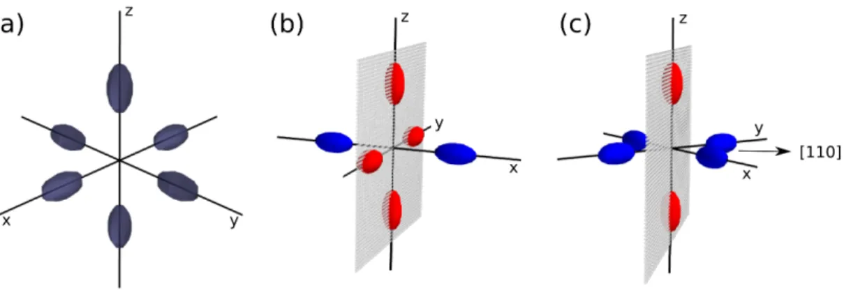
3.3 (a) Bulk Si has six equivalent ellipsoidal energy surfaces around the conduction band minima. The ellipsoids are described by the heavy longitudinal m∗l = 0.92 mo and light transverse m∗t = 0.19 mo masses.
(b) For⟨100⟩-aligned Si NWs four of the six minima stay on the con-finement plane and project to Γ-point. (c) For ⟨110⟩-aligned Si NWs two of the six ones stay on the confinement plane and project to Γ. Those projecting to Γ-point are shown with red whereas the blue ones fold through the NW axial direction. . . 37 3.4 Dispersion curves of 2 nm diameter Si NWs along (a) ⟨100⟩ and (b)
⟨110⟩ directions. For ⟨100⟩ NW both band edges are located at
Γ-point resulting with a direct band gap, whereas for⟨110⟩ NW, the off-Γ minimum leads to an indirect gap. Note that the energy scales are different. As we discuss in Sec. 3.3, the band edges are aligned with respect to those of bulk Si. . . 39 3.5 The folded band structure of bulk Si along the⟨110⟩ direction. A
repre-sentative supercell is filled with only Si atoms so that the band structure of bulk Si is folded. . . 40 3.6 The computational supercells contain (a) two- or (c) three-wire
cross-ings to build up (b) two- or (d) three-dimensional continuous Si NWNs, respectively. The wire orientations are in the family of⟨110⟩ directions. (Reproduced with permission from Ref. [11]. Copyright 2013, AIP Pub-lishing LLC.) . . . 42 3.7 Band gap values for two-wire crossings. The calculated data points are
shown with the markers, the lines are obtained via Eq. (3.2) (β=5.5 is used, see also Table 3.1). The crossing wire alignments are along⟨110⟩ directions. . . 45 3.8 Same as Fig. 3.7 but for three-wire crossings. (Reproduced with
LIST OF FIGURES xvi
3.9 Valence and conduction band offsets for⟨110⟩ three-wire crossings with respect to bulk Si band edges. The calculated values are shown with the markers whereas the estimation values based on the single nanowire parameters are plotted with the curves. Note that the energy scales are different. . . 47
4.1 Schematic view of two representative subbands. The energy level EF
in-tersects the red subband only once, whereas there are two intersections for the blue one. Hence, at this energy level, the red will contribute Go
to the conductance, that is 2Go for the blue subband. . . 54
4.2 The calculated band structure, electronic conductance, and DOS of a
⟨110⟩-aligned Si NW of diameter of 2 nm. . . . 67
4.3 Calculated conductance values reflect the convergence of band disper-sion. (a) Band structure of ⟨110⟩-aligned Si NW of diameter of 2 nm, setting the number of ⃗k⊥-points as 13×13 and k∥-points as 100. (b) the convergence of conductance with respect to number of in-plane ⃗k⊥-points. 68 4.4 Same as Fig. 4.3 but now (b) presents the convergence with respect to
number of k∥-points, setting number of ⃗k⊥-points as 13×13. . . . 69 4.5 The conductance of⟨110⟩-aligned Si NW of diameter of 2 nm. Eq. (4.53)
gives the ideal conductions steps. However, when the momentum ma-trix elements are calculated within the LCBB method by Eq. (A.11) and employed in Eq. (4.51), the ideal steps and plateaus are deformed. 70 4.6 Band structure, conductance and velocity values for the first conduction
and valence subbands originating from Γ-point. LCBB-calculated veloc-ity values [via Eq. (A.11)] deviate from the derivative-derived velocities [via Eq. (4.16)]. The latter, basing on the band structure, indicates the proper values for which the characteristic cancellation of 1D transport satisfies and then ideal conduction steps are displayed. . . 71
LIST OF FIGURES xvii
5.1 Zero-temperature ballistic conductance for 1.5 nm, 2 nm and 2.5 nm di-ameter ⟨110⟩-aligned embedded Si NWs. In the inset, the band edge electron and hole effective masses are given for various diameters in the units of free electron mass mo. . . 74
5.2 Finite temperature ballistic conductance of the⟨110⟩-aligned Si NW of diameter of 2 nm. In the inset, we focus on the VB edge for a variety of low-temperature values to indicate the smearing effect of temperature. 75 5.3 Isosurfaces for charge densities corresponding to the first six/twelve
states below/above the valence/conduction band edges for the three-wire crossing with three-wire orientations along ⟨110⟩ directions and diame-ters of all 1.5 nm. The isosurfaces enclose densities from 100% to 10% of their respective maxima.. . . 76 5.4 Calculated ballistic conductance around (a) VB and (b) CB edges for
several structures such that: first the single Si NW of diameter of 1.5 nm is considered, then the branches are introduced on the NW (see the inset illustration, NW is continuous along the [110] direction, the trun-cated branches are in the other⟨110⟩ directions). By elongating branch lengths, the branching NWs are interconnected with the neighboring supercell images to build up a continuous network. . . 77 5.5 The calculated ballistic electron conductances and energy spectrum of
a 3D NWN of equal wire diameters of all 1.5 nm (same as the network of Fig. 5.4). On top panel, the conductance through the 1D channel of [110] NW is calculated via A1 approach. In the middle panel, within A2 approach, the network is treated with a 3D k-grid, then the transport along the [110] direction is computed. In the bottom panel, the energy spectrum corresponding to middle panel is given. . . 79
LIST OF FIGURES xviii
5.6 Isosurfaces for charge densities corresponding to the first six states be-low/above the valence/conduction band edges for the three-wire cross-ings with wire orientations along⟨110⟩ directions and diameters of 1 nm, 1.5 nm, and 2 nm. The isosurfaces enclose densities from 100% to 10% of their respective maxima.. . . 81 5.7 Isosurfaces for charge densities corresponding to the (a) highest VB
and (b) lowest CB edge states for a⟨110⟩ three-wire crossing with wire diameters of 1 nm, 1 nm, and 3 nm. The isosurfaces enclose densities from 100% to 10% of their respective maxima. Carriers densities extend through the widest crossing wire. . . 82 5.8 Comparison of band gap values (Eg), as well as valence (∆VBO) and
conduction (∆CBO) band offsets with respect to bulk Si band edges for a
branched nanocrystal, branched NW and continuous 3D network. The wire and rod alignments are along⟨110⟩ directions. . . . 84 5.9 A representative kinked NW illustrated from two aspects.The blue and
green segments are along the [110] direction, whereas the red ones are along [100] direction. Regarding also the supercell periodicity along the kinked NW, the shape can be altered by changing: (i) total length of blue segments , (ii) length of red segments, (iii) length of green segment. The supercell contains 1532 Si and in total 13328 atoms. . . 86 5.10 The calculated ballistic electron conductances and energy spectrum of
a KNW of all the segments have diameter of 1.5 nm. On top panel, the A1 approach is exploited to extract the NW-like extended states and their corresponding conductance steps. In the middle panel, within A2 approach, the KNW is treated with a 3D k-grid, then the transport along the [110] direction is computed. In the bottom panel, the energy spectrum corresponding to middle panel is given. . . 87 5.11 Isosurfaces for charge densities corresponding to several conduction
states (CS) of a KNW. The isosurfaces enclose densities from 100% to 10% of their respective maxima.. . . 89
LIST OF FIGURES xix
5.12 Isosurfaces for charge densities of LUMOs of three different shape KNWs. The energy levels of the states are also given in reference to lowest of them. As expected from the quantum confinement, with in-creasing volume of [100] segment the energy value of LUMO decreases. The isosurfaces enclose densities from 100% to 10% of their respective maxima. . . 90
B.1 (a) In the bottom panel, energy spectrum obtained by Eq. (B.2) for the nanowire of infinite potential walls and size of Lx= 1 nm and
Ly= 1 nm. In the top panel, the corresponding DOS is calculated
via Eq. (B.6). To approximate the analytic result, Lz= 100 nm and
Nz= 200 are taken. (b) The zero-temperature dc-conductance of
the NW in the units of 2e2/h. Analytic result is compared with the Gaussian and Lorentzian broadened density of states. The broadening parameter γ= 0.05 eV. . . . 117
B.2 Same as Fig. B.1 but Lz= 5 nm and Nz= 10 are taken to ruin the
step-like conductance. . . 118
B.3 Same as Fig. B.1 but Lz= 100 nm and Nz= 50 are taken to
List of Tables
2.1 Parameters of the pseudopotential form factors [see Eq. (2.22)] of Si and the wide band-gap matrix which represents SiO2. Units are
given in the text. . . 18
3.1 Wire orientation-dependent fitting parameters associated with Eq. (3.1) (also used for Eq. (3.2)) for the main gap energy (C, α) as well as for VB (CVBE, αVBE) and CB (CCBE, αCBE) edge energies. When diameters d
in Eqs. (3.1) and (3.2) are in nm units, the energies come out in units of eV.. . . 36 3.2 Band gap energies for single Si NWs (No. 1, 4, 7) as well as for
two-wire (No. 2, 5, 8, 9) and three-wire crossings (No. 3, 6, 10-14). Non-crossing bandgap value for each case is quoted in brackets. . 44
Chapter 1
Introduction
Semiconductor nanowires (NWs) are functional building blocks at the forefront of nanoscience and nanotechnology due to their controllable synthesis, confined carriers, tunable indirect-to-direct band gaps, and high surface-to-volume ra-tios [12, 13, 14]. Though the appearance of NWs can be traced back to the whiskers of 1960s [15, 16, 17], the bloom of both experimental and theoretical research waited till 1990s for the striking photoluminescence properties of porous silicon (PS) [18, 19]. One of the explanations of blue shift in PS was presented by modeling PS as an array of Si NWs [18, 19, 20, 21, 22, 23]. Shedding light on the quantum size effect and hence the band gap engineering opportunities, the success of the model heralded the promising future of NWs.
Si NW architectures, among all semiconductors, have the upper hand thanks to their inherent integrability and compatibility with the native silicon tech-nology. Single-crystalline Si NWs have been synthesized with various diame-ter distributions, growth orientations and dopant concentrations with various techniques [24, 25, 26, 27, 28, 1, 29]. The advancements in ability to rationally synthesize Si NWs has enabled several applications such as biosensors [30], logic gates [31], lasers [32], electronic [33], photonic [34], photovoltaic [35, 36], and ther-moelectric devices [37, 38].
attention. As the channel length of conventional metal-oxide-semiconductor field-effect-transistors (MOSFETs) shrinks down to nanometer regime, the perfor-mance enhancement by further downscaling becomes questionable mainly due to the short-channel effects [39, 40]. In order to continue the effective minia-turization as captured by Moore’s law [41], the complementary MOS technol-ogy seeks new device architectures in which the bulk MOSFETs are replaced by convenient alternatives. In this regard, Si NW transistors promise a pos-sible solution to the downscaling challenges of MOSFETs thanks to their en-hanced electrostatic controllability and close to the ballistic limit transport ca-pabilities [39]. The reliable fabrications of SiNW FETs have been demonstrated by several experimental studies with NW diameters reaching down to several nanometers [33, 42, 43, 44, 45, 46, 47, 48].
In the sub-10-nm dimension scale, the quantum effects substantially alter the bulk electronic properties and hence the conventional transport features, giving rise to modified band structures, indirect-to-direct band gap transitions, quan-tized conductance, and interference effects, just to name a few. Nevertheless, due to the experimental difficulties in determining the electronic properties of nanostructures [49], it becomes vital to predict them via realistic computational tools. Having a solid understanding of the underlying physics, one can suggest design principles to achieve specific functionalities and indicate the potential per-formance limits.
Various electronic structure calculation methods have been applied to un-derstand the material properties of Si NWs. Particularly, the structure and surface chemistry-dependent electronic properties such as wire diameter, cross-section shape, growth orientation, surface passivation and doping profile are widely investigated [20, 50, 4, 51, 52, 6, 53, 8, 9, 54, 55, 3]. A comprehensive review on the theoretical investigations about structural, electronic, and trans-port properties of Si NWs is given by Rurali [14]. Majority of the theoretical studies have been performed within the first principles density functional the-ory (DFT) [20, 50, 4, 51, 52, 6, 53, 8, 9, 54]. Corrections to the underestimated Kohn-Sham energy gap [56] are introduced by GW approximation [4, 6, 5, 7], hybrid functionals [8, 9] or scissor operation [10]. Alternatively, the electronic
properties can also be computed with the empirical [55, 57, 2, 58] and semiempir-ical [3] methods. These latter methods, with reduced computational load, enable access to Si NWs with diameters reaching up to 10 nm [58].
Among many possible device applications of NWs, the transistors stands at the forefront due to the industrial demands. Therefore, it is not surpris-ing that many of the theoretical efforts on Si NWs have focused on their transport characteristics. Different electronic structure methods have been ex-ploited such as the effective mass approximation, with [59, 60, 61, 62] and without [63, 64, 65, 66, 67, 68, 69, 70, 71, 72, 73, 74, 75, 76, 77, 78] non-parabolic band corrections, ⃗k· ⃗p method [79, 80], tight binding approach [66, 81, 82, 83, 75, 84, 85, 86], and first principles calculations [87, 88, 89], to name a few. Then the resulting band structure information is used to feed the trans-port calculations, relying on semiclassical ballistic model [83], compact model-ing [73, 89, 77], multisubband Monte Carlo technique [60, 74, 75], direct solution of Boltzmann transport equation [62, 71, 70, 85], Kubo-Greenwood formula [63, 76], Landauer-B¨uttiker formula [87, 88, 61, 82, 89], or nonequilibrium Green’s func-tion (NEGF) method [64, 65, 67, 81, 68, 69, 82, 72, 74, 84, 78, 80]. Ballistic transport is expected to play an important role in the electronic performance of NW-based devices [90, 91, 64, 67, 68, 61, 83, 70, 72, 73, 89, 80]. On the other hand, several scattering mechanism can limit the transport, including sur-face roughness scattering [65, 87, 59, 60, 69, 62, 71, 72, 75, 84, 85, 76, 78, 80] as well as phonon [63, 67, 59, 60, 62, 85, 80], Coulomb [59, 76], and impu-rity [88, 62, 74, 75, 85] scattering. Strain engineering [81, 86, 80] techniques can also significantly modify the device performance.
Once the controllable synthesis and physical understanding of NWs advances, as a natural next step, there has been a considerable interest in assembling them into higher dimensional hierarchical architectures as functional building blocks for the next generation devices. En route, after the introduction of branched nanocrystals [92], the branched [93] or tree-like [94] epitaxial NW structures are immediately realized. This is followed by the interconnection of branched nanos-tructures into the large-scale NW networks, in some cases employing different semiconductors [95, 96].
In addition to significant progress achieved in their controllable growth [97, 98], branching structures have been introduced as key components of nanoelectronic devices including light-emitting diodes, logic gates, and biosensors [98]. Branch-ing nanostructures are also discussed and suggested as a central material for the implementation of third-generation photovoltaics, as the branching structures im-prove the light absorption by the increase of absorbing medium, in comparison to conventional NW solar cells; moreover, reduce the light reflectance with in-creasing the effective path for scattered light to travel within the network [99]. In particular, Si NW networks are employed in the fabrication of thermoelectric devices [100], photodetectors [101], and, biosensors [102]. The realization of other proposals, such as multi-terminal electron devices and artificial neural networks are still waiting for the implementation [96, 103].
Yet, there appears to be very limited understanding of the underlying mech-anism to tune the electronic properties of NW networks. More critically, to take the best advantage, fundamentals of carrier collection, separation and transport processes need to be clarified . Besides, the band alignments of these nanostruc-tures are essential for a proper electrical contact design to effectively extract the carriers. Thus, the paradigm brought by branched nanowires for assembling hi-erarchical devices makes it essential to understand the novel physical phenomena in nanoscale crossing-wire structures. By this way, one can address how will the promising NW utilities will be taken over to networks and will networks reveal even new features?
Nevertheless, in contrast to the single SiNWs, only a few theoretical studies have been carried out for the electronic properties of branched Si NWs and NW networks. Menon et al. [104] investigate the branched pristine Si NWs, whereas experimentally grown NWs have always passivated surfaces. Avramov et al. [105] consider some very small size flower-like Si nanoclusters rather than realistic branched Si NWs. In regard to electronic transport in NW networks, since sem-inal work of B¨uttiker [106], many studies have been conducted in the context of quantum transport in multi-terminal junctions, Refs. [107, 108, 109, 110, 111] to name some. Moreover, the NW junctions formed by putting one NW on top
of another one is investigated within a lattice tight binding model in conjunc-tion with the Green’s funcconjunc-tion approach [112]. This work indicates bound and quasi-bound states at around the contact region as a consequence of interwire interaction. The intra- and inter-wire couplings are included with some repre-sentative parameters. Nevertheless, to the best of our knowledge none of the aforementioned works in this field has considered the proper atomistic treatment of NWs. The lack of more realistic theoretical treatment in such an experimen-tally attractive area can be explained by the fact that even the smallest realistic branched systems, including the surface passivation media, contains ∼103–104
atoms in the computational supercell. Though, DFT-based calculations set the benchmark reference for electronic structure calculations, the computational load increases intractably for the realistic branched materials. Therefore, the compre-hensive study of realistic branched structures stands as a great challenge for the first principles methods due to prohibitively increased computational load and requires more feasible semiempirical techniques.
1.1
This Work
The aim of this work is to shed light on several issues raised above, from a theoretical-computational perspective. We present a large-scale atomistic insight into the electronic properties of Si NW-based complex nanostructures, mainly to the networks of Si NWs. This has been achieved by focusing on two aspects: the electronic band structures and quantum ballistic transport. Although these two subjects are Siamese twins, their characteristics extensions invoke separated treatments. In Chapters 2 and 3, we concentrate on the electronic structure calculations. In Chapters 4 and 5, we spotlight the quantum transport features.
Nanostructures are model systems to investigate the manifestations of quan-tum effects due to their unprecedented dimension scales, crystalline purity and perfection. Nevertheless, the experimental limitations on measuring the elec-tronic structure call realistic theoretical tools to assess the fundamental features.
In our computational framework, the semiempirical pseudopotential-based
atom-istic Hamiltonian is solved using an expansion basis formed by the linear
com-bination of bulk bands (LCBB) of the constituents of the nanostructure, i.e., Si and embedding matrix in our case. The formulation of the method and its im-plementation details as well as convergence tests are given in Chapter 2. Being a semiempirical method, LCBB has the advantage that the calculated band gaps of nanostructures reasonably agree with the experimental values whenever avail-able. Yet, the main virtue of the method is that it allows us to deal with systems containing tens of thousands of atoms within a reliable accuracy at the band edge energy landscape.
In Chapter 3, we report our electronic structure results. First, to lay the groundwork for NW networks, we consider embedded Si NWs oriented in ⟨100⟩,
⟨110⟩, ⟨111⟩, and ⟨112⟩ crystalline directions. We compute the band gap energies
as well as valence and conduction band edge alignments with respect to those of bulk Si as a function of NW diameter. Our results are compared with the litera-ture whenever available. In order to interpret the calculated band struclitera-tures, the Brillouin zone folding and indirect-to-direct band gap transitions are discussed. This is followed by a detailed analysis of Si NW networks, composed by regular arrays of NW-crossings, to construct the understanding of their electronic proper-ties. The comprehensive results are consolidated into a general expression which provides an effective way to estimate the electronic band gaps of NW networks. Considering device applications, the band-offsets of Si NWs and NW networks with respect to the band edges of bulk Si and SiO2 are also provided.
To gain more insight into the underlying physics of NW networks and further NW-based complex nanostructures such as kinked NWs, in Chapters 4 and 5, we complement the electronic structure calculations with quantum ballistic trans-port and carrier localization analysis. Accordingly, in Chapter 4, first we give a preliminary discussion of 1D ballistic transport in the context of Landauer for-mula. Then, in the seek of a fully quantum mechanical representation, we derive the Kubo-Greenwood (KB) formula. In the subsequent sections, we indicate the computational implementation details of KG-formula and examine the bridging with the LCBB method. Finally, we revisit the convergence of LCBB calculated
band structure in the light of conductance calculations.
In Chapter 5, after briefly visiting the transport features of single NWs, we proceed with the analysis of isosurfaces of carrier densities to address the impact of crossings and kinks on the electronic behavior. The carrier localization analysis are interpreted together with the ballistic transport calculations to derive conclu-sions on the characteristic features of NW-based complex nanostructures. Based on our results on the band edges and charge profiles, we assert that the results derived for networks are general and apply as well to branched nanocrystals and branched NWs.
To conclude, in Chapter 6, we summarize and discuss our results. We indicate some open questions for the future works. In Appendix A, we show the calculation of momentum matrix elements within the context of LCBB method. Appendix B demonstrates some numerical implementation details of KG-formula on a toy model.
Chapter 2
Mise en sc`
ene: Linear
Combination of Bulk Bands
Method
Reduction of the system dimensions to the nanoscale leads to intriguing quantum behaviors and impacts the device properties rather peculiarly. Due to experi-mental obstacles on measuring the electronic properties of nanostructures [49], it becomes vital to estimate the properties by means of reliable computational tools.
For the electronic structure calculations of large-scale nanostructure systems, Wang and Zunger introduced the linear combination of bulk bands method [113, 114, 115]. The method suggests to expand the states of considered nanostructure in terms of full-zone bulk Bloch bands of the underlying materials, i.e., Si and silica in our case. The main virtue of the method lies in the construction of the expansion basis. The insightful selection of the basis economizes that, and thus enabling to compute even million-atom systems [115]. Basing on a semiempirical pseudopotential Hamiltonian, moreover, the LCBB method embraces the fine details of the atomistic environment.
back to the works of Ninno et al. [116, 117]. Following Wang and Zunger’s for-mulation for self-assembled quantum dots [114, 115, 118] several different groups have successfully implemented the method for various systems such as superlat-tices [119, 120], high-electron mobility transistors [121], Si inversion layer [122], and embedded Si and Ge nanocrystals [123, 124, 125, 126, 11].
LCBB method is originally introduced for the electronic structure calculations of nanocrystals [114, 115]. By this reason, the formulation and implementation details of LCBB are often given for the three-dimensional (3D) supercell case which inherently bases on a 3D reciprocal space representation [114, 115, 123]. In the case of 1D nanostructures, only two of the three translational symmetries are broken, in comparison to nanocrystals, revealing energy dispersion along the continuum direction. In order to compute the proper energy dispersion relation, one needs a modified planar expansion basis set and corresponding separated eigenvalue problems. In this chapter, we emphasize the elaboration of the latter, the organization is such that: in Sec. 2.1, we present the formulation of LCBB method and some guidelines for the computational implementation. An impor-tant aspect of the electronic structure computations is the surface passivation. We describe our passivation recipe in Sec. 2.2. Further details on the expansion basis selection as well as convergence tests are given in Sec. 2.3.
2.1
Formalism
In the wave function expansion methods [56], the states of the nanostructures Ψj(⃗r) are expressed as a linear combination of appropriate basis functions,
Ψj(⃗r) = Nα
∑
α=1
Cα,jϕα(⃗r), (2.1)
where the quantities Cα,j are the expansion coefficients. Form of the basis
tions are specified by the particular method applied, plane waves, Wannier func-tions or atomic orbitals, just to name a few [56]. The number Nαof basis functions
ϕα(⃗r) scales linearly with system size (i.e., the number of atoms) such that the
regard, the LCBB method proposes to overcome this handicap by forming an economic expansion basis which is formed with insightful choices.
As an antecedent to LCBB method, we can consider the ⃗k·⃗p method in which the zone-center Γ (⃗k = 0) bulk Bloch bands {un,0(⃗r)} are employed to form the
expansion basis {ϕα(⃗r) = un,0(⃗r)ei⃗k·⃗r}. Then the states of the nanostructure can
be expanded as Ψj(⃗r) = N∑B,Nk n,⃗k Cn,⃗k,j [ un,0(⃗r)ei⃗k·⃗r ] , (2.2)
where NBis the number of bands and Nkis the number of wave vectors ⃗k included
in the expansion. The inevitable error of the approach is that it is not possible to generate the full-band structure through the Brillouin zone (BZ) unless all (NB =∞) zone-center bulk bands are included [114].
In the LCBB method, the zone-center bands {un,0} in Eq. (2.2) are replaced
with the full-zone bulk Bloch bands{un,⃗k} of the underlying semiconductors of the nanostructure. Within this framework, the nanostructure states can be written as the linear combination of bulk bands, rewriting Eq. (2.2), we get the expansion
Ψj(⃗r) = ∑ n,⃗k,σ Cσ n,⃗k,jϕ σ n,⃗k(⃗r) = ∑ n,⃗k,σ Cσ n,⃗k,j [ 1 √ Nu σ n,⃗k(⃗r)e i⃗k· ⃗r ] , (2.3)
where N is the number of bulk primitive unit cells within the large supercell of the nanostructure, n is the bulk band index, ⃗k is the wave vector belonging to the first BZ of the underlying lattice, and σ is the underlying material index. The periodic part uσ
n,⃗k(⃗r) of the bulk Bloch function can be expanded by the plane
waves as uσn,⃗k(⃗r) = √1 Ωo ∑ ⃗ G Bn⃗σk( ⃗G)ei ⃗G·⃗r, (2.4) where NG is the number of reciprocal lattice vectors (RLVs) ⃗G within an energy
cut-off, and Ωo is the volume of the primitive cell. The bulk expansion
coeffi-cients Bσ
n⃗k( ⃗G) can be calculated by diagonalizing the bulk Hamiltonian for each ⃗k
point. In our computational implementation, the bulk coefficients are computed by employing the empirical pseudopotential method (EPM) which is also very fast, accurate and easy to implement [127, 128]. Moreover, particularly unlike
ab initio calculations, EPM band gaps accurately agrees with the experimental
values by its construction as they are fitted to bulk properties [127].
For the future reference, collecting all the terms, the LCBB expansion of nanostructure states can be expressed as:
Ψj(⃗r) = ∑ n,⃗k,σ Cn,⃗σk,jϕσn,⃗k(⃗r) = ∑ n,⃗k,σ Cσ n,⃗k,j ∑ ⃗ G [ 1 √ V B σ n⃗k( ⃗G)e i(⃗k+ ⃗G)·⃗r ] , (2.5)
where N Ωo = V is the volume of the computational supercell, being periodic in
all three-dimensions.
The LCBB basis yields significant advantages: (i) The off-Γ bulk states (un,⃗k̸=0) of the constituent materials can be directly included in the basis set. Thus, there is no need any more for huge number of Γ-states to be included into the expansion basis of Eq. (2.2). LCBB method differs in this respect form the
⃗k ·⃗p method. The full-band structure inherently comes out in LCBB method. (ii)
Physically more relevant band-edge states are given the priority in the expansion basis. These benefits reduce the size of expansion basis and thereof result with the significantly lowered computational load. This computational efficiency allows us to consider systems with a very large number of atoms. The supercells containing tens of thousands of atoms are easily tractable with the LCBB method.
The total single-particle Hamiltonian of a generic nanostructure with the ki-netic energy and the ionic potential parts, where the latter describes the atomistic environment within the pseudopotential framework, is expressed by
ˆ H = ˆT + ˆVP P =− ¯ h2∇2 2mo + ∑ σ, ⃗Rl,α Wασ( ⃗Rl) υασ(⃗r− ⃗Rl− ⃗dσα) . (2.6)
Here mo is the free electron mass, the direct lattice vector (DLV) ⃗Rl gives the
position of the primitive cell and ⃗dσ
αspecifies the relative coordinate of a particular
atom within the primitive cell. The weight function Wσ
α( ⃗Rl) keeps the information
about the composition of the system by taking values 0 or 1 depending on the type of the atom located at the position ⃗R + ⃗dσ. υσ is the local screened spherical
atomic pseudopotential of atom α of the material σ. In this work, we assume that all the materials forming the nanostructure have the same Bravais lattice. The generation of the method to strained systems can be found in Ref. [115].
In LCBB method, the Hamiltonian matrix elements are evaluated within the basis set {|n⃗kσ⟩} that is {⟨⃗r|n⃗kσ⟩ = ϕσ
n,⃗k(⃗r)} in the position representation. The
resulting Hamiltonian is diagonalized to yield Cσ
n,⃗k,j coefficients. The
correspond-ing generalized eigenvalue problem is ∑ n,⃗k,σ ⟨n′⃗k′σ′| ˆT + ˆV P P|n⃗kσ⟩ Cn,⃗σk,j = Ej ∑ n,⃗k,σ Cn,⃗σk,j⟨n′⃗k′σ′|n⃗kσ⟩ . (2.7)
Let us consider the eigenvalue problem term by term. The right hand side term
⟨n′⃗k′σ′|n⃗kσ⟩ represents the bulk wave function overlap, inserting ˆI =∫ d3r|⃗r⟩⟨⃗r|
into that, we get
⟨n′⃗k′σ′|n⃗kσ⟩ = 1 N ∫ V d3r√1 Ωo ∑ ⃗ G′ Bσ′ n′⃗k′( ⃗G ′)∗e−i(⃗k′+ ⃗G′)·⃗r′ 1 √ Ωo ∑ ⃗ G Bσ n⃗k( ⃗G)e i(⃗k+ ⃗G)·⃗r = 1 N ∫ V d3r 1 Ωo ∑ ⃗ G′, ⃗G Bnσ′′⃗k′( ⃗G′)∗Bn⃗σk( ⃗G)ei(⃗k−⃗k′+ ⃗G− ⃗G′)·⃗r. (2.8) The position vector ⃗r of the supercell can be written as ⃗r = ⃗Rl + ⃗rp where ⃗Rl
are the DLVs of the lattice and ⃗rp is the position vector inside the primitive cell.
This allows us to write ∫V d3r→∑N
l=1 ∫ Ωod 3r p. Thus ⟨n′⃗k′σ′|n⃗kσ⟩ = ∑ ⃗ G′, ⃗G Bnσ′′⃗k′( ⃗G′)∗Bn⃗σk( ⃗G) 1 N N ∑ l=1 ei(⃗k−⃗k′)· ⃗Rlei(G⃗− ⃗G′)· ⃗Rl × 1 Ωo ∫ Ωo d3rpei( ⃗ G− ⃗G′)·⃗rp, (2.9)
using the facts that N1 ∑Nl=1ei(⃗k−⃗k′)· ⃗Rl = δ
⃗k,⃗k′ and Ω1o ∫ Ωod 3r pei( ⃗ G− ⃗G′)· ⃗rp = δ ⃗ G, ⃗G′,
also since ei(G− ⃗⃗ G′)· ⃗Rl = 1, Eq. (2.9) yields
⟨n′⃗k′σ′|n⃗kσ⟩ = δ ⃗k,⃗k′ ∑ ⃗ G Bnσ′′⃗k( ⃗G)∗Bn⃗σk( ⃗G) . (2.10) Notice that the term Ω1
o ∫ Ωod 3r pei( ⃗ k−⃗k′)· ⃗rp
also drop here due to δ⃗k,⃗k′. We employ
The next term kinetic energy matrix elements ⟨n′⃗k′σ′| ˆT|n⃗kσ⟩ in Eq. (2.7) can be treated similarly ⟨n′⃗k′σ′| ˆT|n⃗kσ⟩ = ∑ ⃗ G′, ⃗G Bnσ′′⃗k′( ⃗G′)∗Bσn⃗k( ⃗G)¯h 2|⃗k + ⃗G|2 2mo 1 N N ∑ l=1 ei(⃗k−⃗k′)· ⃗Rlei(G⃗− ⃗G′)· ⃗Rl × 1 Ωo ∫ Ωo d3rpei( ⃗ G− ⃗G′)· ⃗rp, (2.11)
and thus gives
⟨n′⃗k′σ′| ˆT|n⃗kσ⟩ = δ ⃗k,⃗k′ ∑ ⃗ G ¯ h2|⃗k + ⃗G|2 2mo Bnσ′′⃗k( ⃗G)∗Bn⃗σk( ⃗G) . (2.12)
The last term in Eq. (2.7) is the potential energy term ⟨n′⃗k′σ′| ˆVP P|n⃗kσ⟩. To
evaluate the matrix elements first inserting the identity vectors and then using the local pseudopotential property ⟨⃗r| ˆVP P|⃗r′⟩ =
∫ δ(⃗r − ⃗r′)VP P(⃗r)d3r′, we can write ⟨n′⃗k′σ′| ˆV P P|n⃗kσ⟩ = 1 N Ωo ∑ ⃗ G′, ⃗G Bσ′ n′⃗k′( ⃗G ′)∗Bσ n⃗k( ⃗G) ∫ V d3rei(⃗k+ ⃗G−⃗k′− ⃗G′)·⃗r × ∑ σ′′, ⃗Rl,α Wασ′′( ⃗Rl) υσ ′′ α (⃗r− ⃗Rl− ⃗dσ ′′ α ) , (2.13)
and with the change of variable ⃗r = ⃗Rl+ ⃗rp+ ⃗d′′α, we obtain
⟨n′⃗k′σ′| ˆV P P|n⃗kσ⟩ = ∑ ⃗ G, ⃗G′ Bnσ′′⃗k′( ⃗G′)∗Bn⃗σk( ⃗G)∑ σ′′,α Vσ′′ α (|⃗k + ⃗G − ⃗k′− ⃗G′| 2) × Wσ′′ α (⃗k− ⃗k′)ei(⃗k+ ⃗G−⃗k ′− ⃗G′)·⃗dσ′′ α , (2.14)
where the discrete Fourier transforms are defined as
Vσ′′ α (|⃗k + ⃗G − ⃗k′− ⃗G′| 2 ) = 1 Ωo ∫ V υασ′′(⃗rp)ei(⃗k+ ⃗G−⃗k ′− ⃗G′)·⃗rp d3rp (2.15) and Wσ′′ α (⃗k− ⃗k′) = 1 N ∑ ⃗ Rl Wασ′′( ⃗Rl)ei(⃗k−⃗k ′)· ⃗R l. (2.16)
Here, we would like to emphasize an important implementation detail of LCBB method that derives from the definitions of the above discrete Fourier
transformations. As we state earlier, in this work the materials forming the nanos-tructure are assumed to have the same underlying Bravais lattice: ⃗Rn1,n2,n3 =
n1⃗a1+ n2⃗a2+ n3⃗a3 where{⃗ai} are the primitive lattice vectors of the lattice. The
3D periodic boundary conditions dictate that
W ( ⃗Rn1,n2,n3 + Ni⃗ai) = W ( ⃗Rn1,n2,n3) . (2.17)
On the other hand, the discrete Fourier transformation introduced in the treat-ment of weight functionsWσ′′
α (⃗q) = 1 N ∑ ⃗ Rn1,n2,n3 W σ′′ α ( ⃗Rn1,n2,n3)e ⃗ q· ⃗Rn1,n2,n3 requires
ei⃗q·Ni⃗ai = 1, so that the reciprocal space k-griding should have the form
⃗ q→ ⃗qm1,m2,m3 = ⃗b1 m1 N1 + ⃗b2 m2 N2 + ⃗b3 m3 N3 , (2.18)
where{⃗bi} are the reciprocal lattice primitive vectors of underlying bulk
semicon-ductor and mi = 0, 1, . . . , Ni− 1. Eq. (2.18) constitutes a strict relation between
the real and reciprocal space grids. This relation is quite restrictive, in the sense that to increase the number of k-space sampling points (i.e., increasing Ni’s), one
needs to enlarge the size of the supercell in real space due to Eq. (2.17). This pro-cedure will inflate the computational load up to intractable limits. Concerning the rapid k-space convergence of LCBB, this is not a critical issue, nevertheless, it becomes crucial in the case of energy dispersion calculations.
For two-dimensionally confined nanostructures, e.g., NWs, only two of the three translational symmetries are broken, in comparison to nanocrystals, giv-ing rise to the energy dispersion along the other direction. The band structure through the dispersion is essential to understand the physics of the material. In order to extract the energy dispersion at definite k-values along the translational symmetry, we should introduce a proper k-grid that both recognizes the disper-sion direction and keeps the computational load tractable. This can be done by explicitly introducing the symmetry of the nanostructure to the LCBB formal-ism. In detail, considering the symmetry of the system, the three-dimensional real space (reciprocal space) can be separated into (i) planar two-dimensional space
⃗r⊥ (⃗k⊥) coinciding with the perpendicular confinement plane, (ii) one-dimension space ⃗r∥ (⃗k∥) parallel to the translational symmetry. Therefore, the vectors of three-dimensional real ⃗r (reciprocal ⃗k) space can be separated into the
We would like to note that, as the LCBB Hamiltonian is constructed and solved in the reciprocal space, the k-space decomposition turns out to be more critical. Indeed, many of the nanostructures considered in this work enforce the employment of 3D real space, regarding the shape of the structures, wheres the reciprocal space can still be decomposed into perpendicular and parallel compo-nents. LCBB formalism has no restriction this regard. Remarkably, as we are going to see in Ch. 5, the dual k-space treatment, 3D or separated 2D, allows us to gain a more complete understanding of some nanostructures.
The separated k-space approach requires a special treatment in the LCBB formalism. Let us briefly describe that. Following the real and reciprocal space decompositions, DLVs and RLVs can also be decomposed into parallel and per-pendicular components: ⃗R = ⃗R∥+ ⃗R⊥ and ⃗G = ⃗G∥+ ⃗G⊥, respectively. Since we want the energy values at a definite ⃗k∥ value, we drop the sum over ⃗k∥ in Eq. (2.5). That leads to an expansion on a planar k-grid of ⃗k⊥:
Ψj,⃗k ∥(⃗r) = 1 √ V ∑ n,⃗k⊥,σ Cσ n,⃗k⊥,⃗k∥,j ∑ ⃗ G Bσ n⃗k⊥( ⃗G)e i[(⃗k⊥+⃗k∥)+ ⃗G]·⃗r = √1 V ∑ n,⃗k⊥,σ Cn,⃗σk ⊥,⃗k∥,j ∑ ⃗ G Bn⃗σk ⊥( ⃗G)e i(⃗k⊥+ ⃗G⊥)·⃗r⊥ ei(k∥+G∥)r∥. (2.19)
Here, in the summation ⃗k∥ still appears since it keeps the information that ⃗k⊥ is not always at the Brillouin center Γ, but can be shifted to a specific ⃗k∥ point along the Brillouin zone of the nanostructure.
Then the Schr¨odinger equation of LCBB changes from the general form of Eq. (2.7) to a specific form of definite ⃗k∥ such that
∑ n,⃗k⊥,σ ⟨n′⃗k′ ⊥⃗k∥σ′| ˆT + ˆVP P|n⃗k⊥⃗k∥σ⟩ Cn,⃗σk ⊥,⃗k∥,j = Ej(⃗k∥) ∑ n,⃗k⊥,σ Cn,⃗σk ⊥,⃗k∥,j⟨n ′⃗k′ ⊥⃗k∥σ′, n⃗k⊥⃗k∥σ⟩ . (2.20)
This form does not put any restriction on our treatment of matrix elements. We should only need to form a planar k-grid at a specific ⃗k∥ point. This can be easily implemented in our coding by constructing a planar k-grid at Brillouin center,
i.e., ⃗k⊥,Γ then carrying it to k∥ point by ⃗k = ⃗k∥+ ⃗k⊥,Γ (illustrated in Fig.2.6 of Sec. 2.3).
By switching to a planar k-grid and constructing the separated eigenvalue problem of Eq. (2.20), we break the rule of Eq. (2.18). As an example, let us assume that the translational symmetry of the nanostructure is along the ⃗b3
direction. The planar k-grid ⃗k⊥,Γ is formed by setting m3 = 0 and driven by
⃗
qm1,m2,m3 = ⃗b1
m1
N1 + ⃗b2
m2
N2 + ⃗k∥ so that we do not need to increase N3. Then the
separated eigenvalue problems of Eq. (2.20) are solved at definite ⃗k∥ values to obtain the energy dispersion E(⃗k∥).
In regard to Hamiltonian matrix elements of Eq. (2.20), as we are solving the Schr¨odinger equation at a definite ⃗k∥, we have ⃗k⊥ = ⃗k∥+ ⃗k⊥,Γ and ⃗k⊥′ = ⃗k∥+ ⃗k⊥,Γ′ . Moreover, owing to the atomic periodicity of the NW along its axial direction, we can take ⃗Rl = ⃗Rl,⊥ so that the supercell can be scanned with the vector
⃗r = ⃗Rl,⊥+ ⃗rp where we recall that ⃗rp is the position vector inside the primitive
cell. Within this picture, the matrix elements ⟨n′⃗k′⊥⃗k∥′σ′|n⃗k⊥⃗k∥σ⟩ can be written
as ⟨n′⃗k′ ⊥⃗k∥′σ′|n⃗k⊥⃗k∥σ⟩ = N1 ⊥ ∫ V d3r 1 Ωo ∑ ⃗ G′, ⃗G Bnσ′′⃗k′ ⊥( ⃗G ′)∗Bσ n⃗k⊥( ⃗G) × ei(⃗k⊥−⃗k′⊥+ ⃗G⊥− ⃗G′⊥)·⃗r⊥ei(k∥−k′∥+G∥−G′∥)r∥ .
In the NW quantization model we have ⃗r = ⃗R⊥,l + ⃗r⊥,p + ⃗r∥,p so that ⃗r⊥ =
⃗
R⊥,l + ⃗r⊥,p and ⃗r∥ = ⃗r∥,p Also using ∫V d3r →∑N⊥ l=1
∫
Aod
2r
⊥,p∫Lodr∥,p and since
we are at a definite k∥ = k∥′, we can write⟨n′⃗k⊥′ ⃗k′∥σ′|n⃗k⊥⃗k∥σ⟩ elements as ⟨n′⃗k′ ⊥⃗k∥′σ′|n⃗k⊥⃗k∥σ⟩ = ∑ ⃗ G′, ⃗G Bσn′′⃗k′ ⊥( ⃗G ′)∗Bσ n⃗k⊥( ⃗G) 1 N⊥ N⊥ ∑ l=1 ei(⃗k⊥−⃗k′⊥)· ⃗R⊥,l × 1 Ao ∫ Ao d2r⊥,pei( ⃗G⊥− ⃗G′⊥)·⃗r⊥,p 1 Lo ∫ Lo dr∥,pei(G∥−G′∥)r∥ = ∑ ⃗ G′, ⃗G Bσn′′⃗k′ ⊥( ⃗G ′)∗Bσ n⃗k⊥( ⃗G) δ⃗k⊥,⃗k′⊥δG⃗⊥, ⃗G′⊥δG∥,G′∥ = ∑ ⃗ G Bnσ′′⃗k′ ⊥( ⃗G) ∗Bσ n⃗k⊥( ⃗G) δ⃗k⊥,⃗k⊥′ , (2.21)
where we exploit the identities that ei( ⃗G⊥− ⃗G′⊥)· ⃗R⊥,l = 1, 1 N⊥ ∑N⊥ l=1e i(⃗k⊥−⃗k′⊥)· ⃗R⊥,l = δ⃗k⊥,⃗k′ ⊥, 1 Ao ∫ Aod 2r ⊥,pei( ⃗G⊥− ⃗G′⊥)·⃗r⊥,p = δ⃗ G⊥, ⃗G′⊥ and 1 Lo ∫ Lodr∥,pe i(G∥−G′∥)r∥ = δG∥,G′∥.
In regard to computational implementation, since we are solving the Schr¨odinger equation at a specific ⃗k∥, we already have an intrinsic δ⃗k
∥,⃗k′∥ that
again allows us to write δ⃗k⊥,⃗k′
⊥ → δ⃗k,⃗k′. Hence, actually Eqs. 2.10 and 2.21 come
up with the same form. That is similar for the kinetic and potential energy matrix elements. Therefore only giving a planar k-grid is enough to run the 3D k-grid based implementation for 2D k-grid case of 1D translational structures. Further discussion about the k-space construction and sampling is given in Sec. 2.3.
2.2
Oxide Passivation and Atomic
Pseudopo-tentials
An important aspect of the electronic structure calculations is the surface passi-vation. The surface of an unpassivated nanostructure consists of dangling bonds which introduces surface states. These localized states lie in the otherwise for-bidden band gap. Surface passivation removes these surface states. From the transport point of view, the passivated surface eliminates the carrier recombina-tion centers and hence enhances the current flow. Actual grown Si NWs samples have passivated surfaces achieved usually either by oxidation or hydrogenation. The latter is rather simple to model computationally: Each Si dangling bond is terminated by forming a stable one layer Si-H binding. The representation of oxide passivation is more difficult, since a large number of atoms is need to de-scribe the thick oxide layer [14]. For this reason, in the study of Si NWs, mostly H-passivation is used as a viable approximation to the oxide passivation [20, 50]. Without increasing the computational cost, instead of H some different materials are also employed to terminate the dangling bonds such as Br, Cl, I [51], OH, NH2[53, 52], and F [9]. However, due to the practical instabilities of these
passi-vations, the calculations of oxide passivated Si NWs becomes essential. For the realistic oxide-passivation, a first principles study of amorphous oxide sheathed
Table 2.1: Parameters of the pseudopotential form factors [see Eq. (2.22)] of Si and the wide band-gap matrix which represents SiO2. Units are given in the text.
a1 a2 a3 a4 a5 a6
Si 106.0686 2.2278 0.606 -1.972 5.0 0.3 Matrix-Si 69.625 2.614 0.0786 -19.1433 5.99 0.335
thin Si NWs has been reported [129]. As reported in this work there can be sub-tle differences between the H- and oxide-passivations, such as in the band gap orderings of different orientation Si NWs.
In our implementation, the surface passivation is provided by embedding the NW structures into a host matrix, being usually silica. However, the EPM cal-culations for oxygen is quite troublesome and, yet more, the different lattice structure of SiO2, with reference to Si, causes strain effects. To overcome these
obstacles, we propose an artificial wide band gap material that computationally substitutes silica. In detail, after constructing the Si NW core, all the remain-ing crystal points within the computational supercell are filled with the artificial
oxide atoms. This artificial embedding material has the same dielectric constant
of SiO2 and band edge lineup, with respect to Si, however with the diamond
structure to prevent complications associated with strain [123].
For the local empirical pseudopotentials of Si and SiO2, we use the
func-tional form introduced by Freidel et al. [130] These authors suggest an analytical expression to produce the pseudopotential form factor at a given general wave number q VP P(q) = a1(q2 − a2) ea3(q2−a4)+ 1 [ 1 2tanh ( a5− q2 a6 ) +1 2 ] . (2.22)
We employ their parameters for Si (listed in Table 2.1) [130]. On the other hand, we have generated new pseudopotential parameters for the artificial SiO2
which reproduces the experimental band alignments of bulk Si/SiO2 interface as
4.4 eV and 3.4 eV for the valence [131] and conduction [132] band edges, re-spectively. The parameter generation is performed via the simulated annealing
optimization method [133, 134] starting from those of bulk Si. The correspond-ing parameters are given in Table 2.1. The units are arranged such that the pseudopotential form factors come out in Rydbergs and the wave number q in Eq. (2.22) should be in the atomic units (1/Bohr radius). For the plane-wave cut-off energies of EPM, we use 14 Ry for both Si and artificial SiO2. The
resul-tant bulk band structures for Si and artificial oxide matrix are plotted in Fig. 2.1. To give a comparison DFT-produced band structure of bulk Si is also given in Fig. 2.1. The band gap of the latter is set equal to EPM band gap by a scissor operation.
Figure 2.1: EPM band structures for bulk Si (blue) and artificial wide band gap matrix (green) together with DFT bandstructure of Si (red) with band gap error corrected.
We note that in our oxide passivation approach, there is an arbitrariness on the pseudopotential representation of the wide band gap material. To overcome this arbitrariness, we checked the oxide passivation with different pseudopoten-tials, all satisfying the same Si/SiO2 interface. We observed that although the
calculated band gap values might vary slightly, the electronic energy and trans-port characteristics that we discuss in the following chapters are robust.
Though the surface chemistry of oxide-passivation requires more elaborate first principles calculations, considering today’s DFT computation limits, we be-lieve that our approach offers a viable alternative for the calculations of oxide-embedded large scale Si nanostructures.
Despite the missing surface relaxation and strain effects, the reliability and competence of our computation method has gained confidence, in the context of embedded Si and Ge nanocrystals, comparing with experimental data for the linear [123] and third-order nonlinear optical properties [124, 135], the quantum-confined Stark effect [126] as well as for the Auger recombination and carrier multiplication [125].
2.2.1
Filtering of oxide-derived surface states
Strictly speaking, the “good” artificial oxide is generated with the intension to remove all surface states which lie in the otherwise forbidden band gap. We observed that the oxide matrix can meet this purpose unless the matrix Bloch functions BSiO2
n⃗k are included into the expansion basis of LCBB [see Eq.(2.5)].
Note that even when we do not include the matrix Bloch functions into the expansion basis, the system Hamiltonian still “knows” the existence of oxide medium thanks to the weight functions and pseudopotential terms [referring to Eq. (2.6)].
Fig. 2.2 shows the calculated energy spectra for an embedded silicon nanocrys-tal of diameter of 1.6 nm for the case that the oxide Bloch functions BSiO2
n⃗k are
included to the LCBB expansion basis. In this part we consider nanocrystals, as surface-to-volume ratio is larger in comparison to NWs, the surface effects are more dominant. Although the band gap is consistent with the result of other electronic structure methods and experiment [123], there is a subtle problem here. As we look for the density of states, we notice that there is a premature oxide continuum in valence band (VB) energies at about -2.5 eV. From our SiO2 matrix
generation, we know that the VB edge of SiO2 matrix should be around -5.4 eV.1


![Figure 3.1: Band gap energies as a function of diameter for [100], [112], [110], and [111]- [111]-oriented Si NWs](https://thumb-eu.123doks.com/thumbv2/9libnet/6017673.126971/53.892.261.697.182.535/figure-band-gap-energies-function-diameter-oriented-nws.webp)