2211 J. Phys. D: Appl. Phys. 31 (1998) 2211–2218. Printed in the UK PII: S0022-3727(98)92917-5
Hydrodynamic approach for
modelling transport in quantum well
device structures
C Besikci†, B Tanatar‡ and O Sen†
†06531Electrical Engineering Department, Middle East Technical University,Ankara, Turkey ‡ Physics Department, Bilkent University, 06533 Ankara, Turkey
Received 1 April 1998, in final form 27 May 1998
Abstract. A semiclassical approach for modelling electron transport in quantum well
structures is presented. The model is based on the balance equations governing the conservation of particle density, momentum and energy with Monte Carlo (MC) generated transport parameters. Three valleys of the conduction band, size quantization in the 0 valley, and the lowest two subbands in the quantum well are considered by taking the detailed intersubband dynamics into account. The transport parameters of the model are extracted from steady-state MC simulations based on an improved formulation of two-dimensional polar optical phonon scattering including screening effects. The predictions of the proposed model have been found to be in excellent agreement with those of the ensemble MC simulations under both time varying and spatially nonuniform fields. The calculated transport parameters which are of interest for device modelling are presented as a function of the electron energy for the AlGaAs/GaAs quantum well. The model serves as an accurate semiclassical alternative to costly ensemble MC simulations for studying the transport in quantum well structures and for the modelling and optimization of submicron devices based on these structures, such
as modulation doped field-effect transistors (MODFETs).
1. Introduction
With recent developments in modern epitaxial growth techniques, III–V heterostructures have received increasing attention for high-performance electron devices such as modulation doped field-effect transistors (MODFETs) and optical devices such as quantum well photodetectors and lasers. The superiority of these devices over conventional ones has been confirmed both theoretically and experimentally. In order to optimize the device operation and use the desirable transport properties of the two-dimensional electron gas (2DEG) efficiently, one must have a sound understanding of the physics of carrier transport in 2D systems. Phonon, impurity and alloy scattering mechanisms in 2DEGs have been extensively studied [1–6]. Following these studies, steady-state and transient ensemble Monte Carlo (MC) simulations have been carried out to determine the 2DEG velocity characteristics in modulation doped heterostructures [7–9], and various models have been
introduced for the simulation and optimization of MODFETs [10–20]. A review of these models has been presented by Salmer et al [21]. Earlier analytical models based on the drift–diffusion formulation were one-dimensional and neglected hot electron effects which become increasingly important as the device dimensions are reduced. The MC technique, which is the
1998 IOP Publishing Ltd most powerful and complete method in device analysis, has also been widely used in the simulation and optimization of MODFETs [18–20]. However, this method is expensive in terms of computer time and faster methods are needed in most applications.
Balance or conservation equations for particle density, momentum and energy are well known in device analysis. The equations are derived from the first three moments of the Boltzmann transport equation. Various forms of the equation set were presented by Blotekjær considering two conduction band valleys [22]. Simpler models have been proposed by extending the conventional drift–diffusion formulation to take nonstationary transport effects into account [23,24]. However, there has been some concern
over the accuracy of these equations in device modelling [25]. Providing substantial information on the physics of carrier transport and being able to model high-field carrier dynamics accurately, the model based on balance equations has been used as a reliable alternative to costly MC simulations in order to model electron devices such as MESFETs, heterojunction bipolar transistors (HBTs) and impact avalanche transit-time diodes (IMPATTs) [26–29]. In most applications, further approximations to Blotekjær’s model were introduced. One of the most widely adopted approximations is the single electron gas approach which averages the quantities of interest over the conduction band valleys. This approach uses only two lumped relaxation times for momentum and energy, leading to loss of detail in the description of intervalley dynamics. In some other applications, the third (X) valley of the conduction band is ignored to keep the number of the energy dependent relaxation times at a manageable level. Recently, we proposed an improved description for the collision terms of the three-valley version of the model by reducing the total number of the relaxation times in the model [30].
While there has been considerable effort to apply the balance equation approach to conventional device modelling, there have not been many attempts to model the transport in quantum well structures by this method. Wang and Hsieh [31] applied the balance equation approach to MODFET modelling by using the single electron gas approach. However the authors extracted the momentum and energy relaxation times from MC simulations on bulk material neglecting the 2D quantization of the electron gas. Widiger et al [14] presented a model based on hydrodynamic-like equations, taking conduction only in the lowest single subband and that in the bulk into account. Darling [32] used Blotekjær’s model [22] to describe transport in a quantum well by considering the quantized electrons and the lowest two subbands only.
In this paper we present a model which considers conduction in both the quantum well and in the bulk by taking the detailed intersubband dynamics and intervalley transfer to the L and X valleys into account. We also confirm the model accuracy by comparing the responses of the model with those of ensemble MC simulations under both time varying and spatially nonuniform electric fields for the Al0.3Ga0.7As/GaAs quantum well. The results of this work show that suitably chosen balance equations with transport parameters determined from homogeneous and steady-state MC simulations can be used to accurately describe the transport in quantum wells under nonhomogeneous, time dependent fields. Section 2 describes the model. The MC procedure is presented in section 3. In section 4, a comparison of the model predictions with those of ensemble MC simulations is given, and finally conclusions are presented in section 5.
2. Model
For a proper description of transport in a quantum well structure such as a MODFET, 2D quantization and intersubband dynamics, intervalley transfer and hot electron
effects should be taken into consideration. In our transport model, we take size quantization in the 0 valley into account and include the lowest two subbands in the model. We consider the higher energy bands to have 3D properties and use an equivalent single valley approach to represent 3D 0, L and X valleys. The 3D approximation is justified for the L and X states due to the much smaller spacing of the energy levels when compared with those at the 0 valley and due to the collision broadening by intervalley scattering [5]. The third and higher subbands in the Al0.3Ga0.7As/GaAs quantum well may not be spaced closely enough to be considered as a quasicontinuum like the case in bulk material; therefore a 3D approximation for the third and higher subbands is not fully justified for the 0 valley. However, as will be shown in section 3, these bands do not play a primary role in transport through the quantum well since significant intervalley transfer to the L valley starts once the electron energy is high enough to populate the third subband. Therefore, there are three electronic subsystems in our model which includes the electrons in the first and second subbands and those with 3D properties.
Taking the first three moments of the Boltzmann transport equation, the expressions that govern the conservation of particle density, carrier momentum and
energy in a 2D electron system can be expressed as (1)
(2)
(3)
For a complete description of the quantized electron system, this equation set must be used for each subband. In these expressions, subscript i refers to the subband in which the carriers reside. q is the electron charge, kB is the Boltzmann constant, E is the electric field, κ is the heat conductivity of the electron gas, n refers to the 2D electron density, v is the
Hydrodynamic model of e transport in QW devices¯
2213 average carrier velocity and w is the average carrier energy.
The terms with the subscript c represent the influence of the scattering processes. We use two sets of these equations, one set for each subband, to model transport in the quantum well. In this case one more equation set for the 3D electron system is needed to complete the system of equations. The third set consists of the 3D version of the balance equations:
(4 ) (5 ) (6 ) Using the relaxation time approximation and extending Blotekjær’s approach [22] for three systems of electrons, the collision terms of the balance equations for particle density and momentum can be phenomenologically
described as
. (8)
Subscripts i, j and k represent the three electron systems. τnij(wi) is the particle density relaxation time due to scattering from system i to j, and τpi(wi) represents the momentum relaxation time in system i due to intersystem and intrasystem scattering. It has been assumed that intersubband and intervalley scatterings are isotropic and completely randomize the carrier momentum. Therefore, equation (8) does not contain a term representing the momentum contribution to system i due to scattering from other systems.
In representing the collision term in the energy conservation equation, we represent the energy relaxation due to intersystem scattering by using particle density
relaxation times instead of intersystem energy relaxation times [30]. In this case, the collision term for the energy conservation equation of system i can be expressed as
(9) τwii(wi) represents the energy relaxation time due to intrasystem scattering in system i, and the first term on the right-hand side describes the relaxation of energy in this system due to intrasystem scattering. wij(wi) stands for the average energy of the transferred electrons from system i to system j just before transfer occurs. eji(wj) is the average energy of the transferred electrons from system j to system i, just after the transfer, excluding the kinetic energy gained or lost due to the difference between the energy minima of the systems which is represented by 1ji = Ej − Ei. The second and the third terms describe the change in the average energy of system i due to the transfer of electrons from this system to systems j and k respectively. The fourth and fifth terms govern the change in the average energy of system i due to the transfer of electrons from systems j and k to this system respectively.
Note that in describing 3D transport in a semiconductor with sufficient energy difference between the minima of the conduction band valleys, eji can be approximated by wji. This approach, which lowers the total number of transport parameters in the model, neglects the effect of intervalley phonon energy on the energy exchange between the electron systems. Since the probability of emission is generally larger than that of absorption, the net effect of the phonon energy on energy exchange is not zero. However, this approach may still be a reasonable approximation if wji +1ji is much larger than the intervalley phonon energy in the energy range where intervalley scattering becomes important, as is the case for 3D transport in GaAs [30]. In our case, since the difference between the subband energies [5] is comparable to the phonon energy, this approximation was not used. We extracted the transport parameters of the model from steady-state MC simulations; the details will be explained in the next section.
3. Monte Carlo simulations and transport parameter extraction
The transport parameters of the model were determined for the Al0.3Ga0.7As/GaAs modulation doped heterostructure by following the trajectory of a single electron in the quantum well for a sufficiently long period of time through a steady-state MC simulation. The simulation was repeated for various uniform electric field strengths corresponding to different steady-state electron energies in order to determine the energy dependence of the transport parameters. Three valleys of the conduction band (0, L and X) and band nonparabolicities were included by considering size quantization in the 0 valley and the first three subbands in the quantum well. Electrons residing in the L and X valleys
and those with energies larger than the third subband were assumed to have 3D properties. Quantum well parameters and the corresponding bandstructure were taken from [5]. After launching the electron in the 2D system, the trajectory of the electron subjected to 2D scattering mechanisms is followed, and it is placed in the 3D system once it is scattered to the third subband or to the L and X valleys. After the electron enters the 3D system, it is subjected to 3D scattering mechanisms until it is scattered back to the 2D system. A similar way of 2D to 3D coupling was used by Park and Brennan [20] in their MC simulations. However, their approach ignored the third and higher subbands, and placed the electron in the 3D system after the electron’s energy exceeded the band bending energy. We have seen that including the third subband in describing the intersubband scattering processes yields more accurate results. We have obtained good agreement between the results of our MC simulations and those of Yokoyoma and Hess [5] who included five subbands in the quantum well. The scattering mechanisms included in the simulation are polar optical phonon scattering, acoustic phonon scattering and intervalley (equivalent and nonequivalent) scattering. We neglected impurity scattering due to background and remote impurities. The scattering rates given by Fawcett et
al [33] were used for 3D electrons.
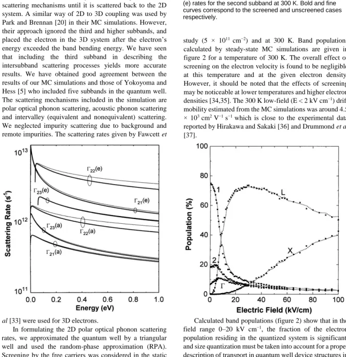
In formulating the 2D polar optical phonon scattering rates, we approximated the quantum well by a triangular well and used the random-phase approximation (RPA). Screening by the free carriers was considered in the static limit, since conservation of energy and momentum restricts the interaction to long wavelengths and hence to low frequencies. We assumed bulk phonons and used Fermi’s Golden Rule with the electron–phonon matrix elements to calculate the scattering rates. Formulation of the 2D polar optical phonon scattering rates, including the effects of screening, will be presented elsewhere [34]. The effects of screening on the 2D acoustic phonon scattering were ignored.
The emission and absorption rates of polar optical phonon scattering for the second subband are given in figure 1. The scattering rates obtained when screening is ignored are also shown for comparison. For all subbands, except for intrasubband scattering, we observed that screening has little effect on the polar optical phonon scattering rates for the 2D electron density used in this
Figure 1. Polar optical phonon absorption (a) and emission
(e) rates for the second subband at 300 K. Bold and fine curves correspond to the screened and unscreened cases respectively.
study (5 × 1011 cm−2) and at 300 K. Band populations calculated by steady-state MC simulations are given in figure 2 for a temperature of 300 K. The overall effect of screening on the electron velocity is found to be negligible at this temperature and at the given electron density. However, it should be noted that the effects of screening may be noticeable at lower temperatures and higher electron densities [34,35]. The 300 K low-field (E < 2 kV cm−1) drift mobility estimated from the MC simulations was around 4.5 × 103 cm2 V−1 s−1 which is close to the experimental data reported by Hirakawa and Sakaki [36] and Drummond et al [37].
Calculated band populations (figure 2) show that in the field range 0–20 kV cm−1, the fraction of the electron population residing in the quantized system is significant, and size quantization must be taken into account for a proper description of transport in quantum well device structures in this field range. It can also be seen that the electron population in the 3D 0 band is insignificant throughout the entire field range, showing that considerable electron transfer to the L valley starts once the electron energy in the quantized system is large enough to populate the third subband. From these results it can be inferred that taking only the two subbands into account and treating the electron as a 3D electron once it is scattered to the third subband is a
Hydrodynamic model of e transport in QW devices¯
2215 reasonable approximation for the analysis of AlGaAs/GaAs
device structures.
3.1. Transport parameters
The transport parameters of the model were obtained as a function of the electron energy from steady-state MC simulations performed under different electric field
Figure 2. Subband 1 (1), subband 2 (2), 3D 0 valley (0), L
valley (L) and X valley (X) populations versus electric field at 300 K.
strengths corresponding to different electron energies. The particle relaxation time, τnij, was estimated using the following relation [26]
(10) where Fi(wi) is the fraction of electron population residing in system i, T is the simulation time, and Nij is the total number of scattering mechanisms from system i to j during the simulation. For the particle density, relaxation times for scattering between the subbands and the 3D system (τn13 and τn23), Ni3 (i = 1, 2) were calculated by summing the number of scatterings from subband i to 3D 0, L and X valleys. The expression for the momentum relaxation time, τpi, was obtained by using [38]
(11) where piss(wi) represents the steady-state average carrier momentum in system i, corresponding to the field E. The energy relaxation time τwii is estimated by using the steady-state and homogeneous form of equations (3) and (9). Determination of wij and eij from MC simulations is straightforward. Note that the effective mass of the electrons in the 3D system is also energy dependent due to the single equivalent valley approach used to represent this system. This dependency is estimated from MC simulations by using the following expression
(12) where F0, FL and FX are the fractions of the electron population residing in 0, L and X valleys respectively.
the average electron energy in this system.
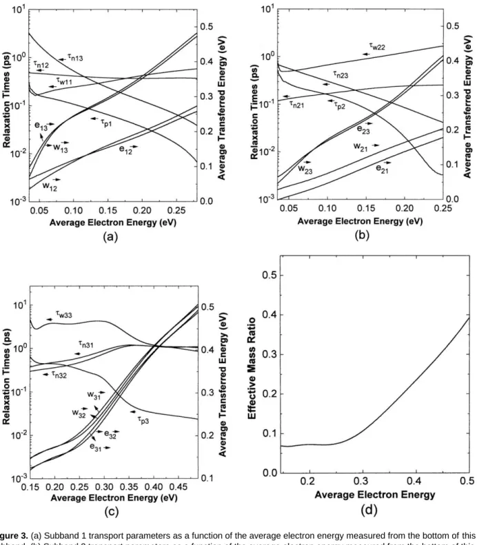
The smoothed transport parameters for the three electron systems as a function of average electron energy in the corresponding system at 300 K are shown in figure 3. Under low electron energies scattering between the first two subbands dominates, and τn12 is smaller than τn13 as can be seen in figure 3(a). However, under moderately large energies τn12 significantly exceeds τn13, although the scattering rate from the first subband to the second subband is always larger than the scattering rate from the first
subband to the third subband whose energy defines the boundary between the 2D and 3D systems in our approach. However, note that we use an equivalent valley approach for the 3D system and, in addition to scattering from the first to the third subband, significant electron transfer starts from the first subband to the L and X valleys under a sufficiently large electron energy in subband 1. In this case, for an electron in subband 1, the probability of scattering to the 3D system is larger than that of scattering to the second subband.
Figure 3. (a) Subband 1 transport parameters as a function of the average electron energy measured from the bottom of this
subband. (b) Subband 2 transport parameters as a function of the average electron energy measured from the bottom of this subband. (c) Transport parameters of the 3D electron system as a function of the average electron energy in this system. The energy is averaged over the 3D 0, L and X valleys. (d) Effective mass ratio of the 3D electron system as a function of
Hydrodynamic model of e transport in QW devices¯
2217 are always larger than e , e and e respectively since
scattering from higher energy states to lower energy states occurs mostly by emission throughout the entire energy range. The energy dependence of the intrasystem energy relaxation times for subbands 1 and 2 suggests that energy in the quantized system is mostly relaxed by intrasubband scattering under low electron energies. Hence, the probability of intrasubband scattering is larger than the probability of scattering to a higher subband, if the electron energy is low. As the electron energy is increased, both intersubband scattering and scattering from the subbands to L and X valleys start, and these processes become dominant in the relaxation of energy.
While it is straightforward to include impurity scattering in the simulations [5], we ignored this scattering mechanism in our calculations. Impurity scattering rates in a modulation doped heterostructure with an undoped spacer layer are likely to be much smaller than the other scattering rates [5].
This scattering mechanism is expected to be considerable by lowering the momentum relaxation times only at low electron energies and at low temperatures.
Figure 5. (a) System populations versus time in response to
a ramped field. (b) Average electron velocity and energy versus time in response to the ramped field shown in (a). The velocity and energy are averaged over the three electron systems.
4. Performance evaluation
4.1. Simulations under spatially uniform, time varying fields
In order to evaluate the accuracy of the model in describing nonstationary transport which becomes significant in submicron devices, the model was tested under time varying and spatially uniform fields. This provides a convenient way
Figure4. Systempopulationsandaverageenergyversus timeinresponsetoastepfield.Theenergyisaveraged overthethreeelectronsystems.
Underlowelectronenergies e 12 exceeds 12 ,sincethe electronsarescatteredfromthefirsttothesecondsubband mostlybyabsorption. However,underlargerenergies, emissionstartsand 12 exceeds e 12 duetotherelatively largerateofemission.Theenergydependenceof e 13 , 13 ,
23 and e 23 canbeinterpretedsimilarly: 21 , 31 and
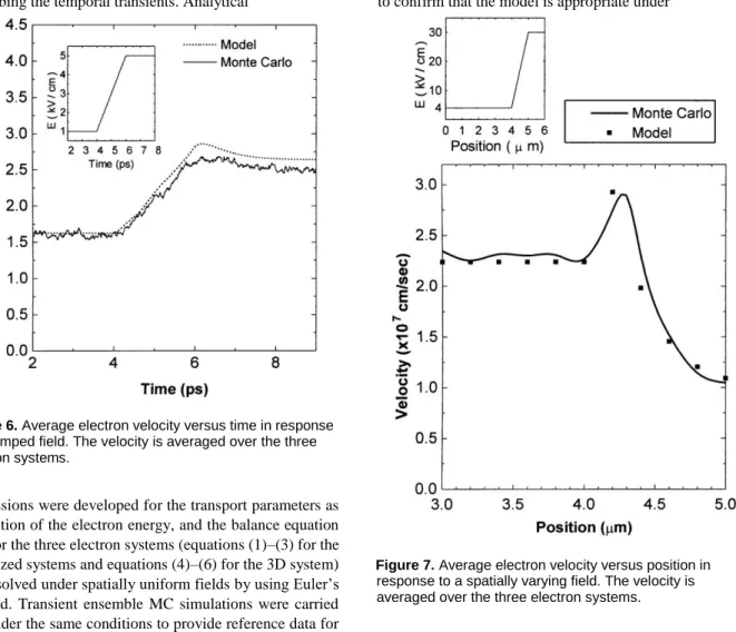
to investigate the reliability of the collision expressions in describing the temporal transients. Analytical
Figure 6. Average electron velocity versus time in response
to a ramped field. The velocity is averaged over the three electron systems.
expressions were developed for the transport parameters as a function of the electron energy, and the balance equation sets for the three electron systems (equations (1)–(3) for the quantized systems and equations (4)–(6) for the 3D system) were solved under spatially uniform fields by using Euler’s method. Transient ensemble MC simulations were carried out under the same conditions to provide reference data for comparison. Figure 4 shows the populations of subband 1, subband 2 and the 3D system (including 0, L and X valley electrons) versus time under a step field. Excellent agreement is achieved between the response of the model and that of MC simulations. Figure 4 also shows the overall electron energy (averaged over the three systems). We found good agreement for both steady-state and transient parts of the transport.
Figure 5 shows the system populations (a) and overall electron velocity and energy (b) (both averaged over the three systems) versus time when a ramped field is applied. The duration of velocity overshoot is very well estimated by the model. The peak velocity predicted by the model is slightly larger than that estimated by the MC method. Nevertheless, the maximum error is around 10%. Simulation results for transient velocity under a relatively low ramped field are shown in figure 6. Both the peak velocity and the duration of the velocity overshoot are estimated with less than 10% error by the model. The results presented above confirm the reliability of the model in describing intersubband and intervalley dynamics.
4.2. Simulations under spatially nonuniform fields In the simulations presented above the model was tested under time varying but spatially uniform conditions. Under
spatial nonuniformity, diffusion effects take place. In order to confirm that the model is appropriate under
Figure 7. Average electron velocity versus position in
response to a spatially varying field. The velocity is averaged over the three electron systems.
these conditions, the balance equation sets were solved under spatially nonuniform fields, and the results were compared with the ensemble MC response. Under spatial nonuniformity, the terms involving the space gradients must be retained in the balance equations. The solution method used in this study is an explicit finite difference scheme similar to that reported by Mains et al [39]. A practically stable solution was achieved with a space step of 0.2 µm and a time step of 5 fs. Figure 7 shows the overall velocity profile of the electrons subjected to a strong field gradient. Both the peak velocity and the width of the velocity overshoot region are well estimated by the model.
5. Conclusion
We have presented a study of electron transport in AlGaAs/GaAs quantum well structures, and a semiclassical model based on the balance equations to describe transport in such structures. We considered size quantization in the 0 valley and the two lowest subbands. Electrons with energies larger than the third subband energy were considered to have 3D properties, and we used an equivalent valley approach to represent 3D 0, L and X valleys. The response of the model to rapid variations of electric field in time and space was
Hydrodynamic model of e transport in QW devices¯
2219 compared with the predictions of ensemble MC simulations
and excellent agreement was achieved. The results show that the model, with the proposed collision terms, provides an efficient alternative to costly MC simulations for studying the physics of transport in submicron quantum well device structures and for device optimization. Furthermore, we found that the transport parameters determined by steady-state homogeneous MC simulations can model nonstationary transport in a quantum well with substantial accuracy. A discussion on the reliability of the relaxation times generated by this technique for 3D transport in the single electron gas approximation has been presented by Sandborn et al [40].
Unfortunately, it is not possible to verify the accuracy of the model and the transport parameters by a direct comparison with experimental observations. There have been several experimental studies on hot electron transport properties of modulation doped AlGaAs/GaAs heterojunctions [37,41]. However, these studies were mainly limited to the measurement of the steady-state velocity–field characteristics and the mobility of the 2D electron gas by I–V and pulsed Hall measurements. The difficulties encountered in the measurements due to the negative differential resistance property generally limit the maximum electric field to the critical field above which intervalley transfer starts.
For ultrasmall devices, quantum interference effects may be important. In order to take these effects into account, improvements to the model can be made by incorporating quantum corrections as proposed by several groups [42–44].
Acknowledgments
This work is supported by the Scientific and Technical Research Council of Turkey (TUBITAK) through contract¨ no EEEAG-168. BT is supported by TUBITAK under grant¨ no TBAG-AY/123.
References
[1] Ridley B K 1982 J. Phys. C: Solid State Phys. 15 5899 [2] Price P J 1981 Ann. Phys. 133 217
[3] Price P J 1982 Surf. Sci. 113 199 [4] Hess K 1979 Appl. Phys. Lett. 35 484
[5] Yokoyama K and Hess K 1986 Phys. Rev. B 33 5595 [6] Basu P K and Nag B R 1983 Appl. Phys. Lett. 43 689 [7] Tomizawa M, Yokoyama K and Yoshii A 1984 IEEE
Electron Device Lett. 5 464
[8] Yoon K S, Stringfellow G B and Huber R J 1987 J. Appl. Phys. 62 1931
[9] Yoon K S, Stringfellow G B and Huber R J 1988 J. Appl. Phys. 63 1126
[10] Drummond T J, Morkoc H, Lee K and Shur M 1982 IEEE Electron Device Lett. 3 338
[11] Park K and Kwack K D 1986 IEEE Trans. Electron Devices 33 673
[12] Wang G W and Ku W H 1986 IEEE Trans. Electron Devices 33 657
[13] Kim Y M and Roblin P 1986 IEEE Trans. Electron Devices
33 1644
[14] Widiger D, Kizilyalli I C, Hess K and Coleman J J 1985 IEEE Trans. Electron Devices 32 1092 [15] Tang J Y F 1985 IEEE Trans. Electron Devices 32 1817 [16] Yoshida J and Kurata M 1984 IEEE Electron Devices Lett.
5 508
[17] Loret D 1987 Solid-State Electron. 30 1197
[18] Tomizawa K and Hashizume N 1988 IEEE Trans. Electron Devices 35 849
[19] Ravaioli U and Ferry D K 1986 IEEE Trans. Electron Devices 33 677
[20] Park D H and Brennan K F 1989 IEEE Trans. Electron Devices 36 1254
[21] Salmer G, Zimmerman J and Fauquembergue R 1988 IEEE Trans. Microwave Theory Technol. 36 1124
[22] Blotekjær K 1970 IEEE Trans. Electron Devices 17 38 [23] Thornber K K 1982 IEEE Electron Device Lett. 3 69 [24] Artaki M 1988 Appl. Phys. Lett. 52 141
[25] Blakey P A, Burdick S A and Sandborn P A 1988 IEEE Trans. Electron Devices 35 1991
[26] Mains R K, Haddad G I and Blakey P A 1983 IEEE Trans. Electron Devices 30 1327
[27] Tomizawa K and Pavlidis D 1990 IEEE Trans. Electron Devices 37 519
[28] Feng Y and Hintz A 1988 IEEE Trans. Electron Devices 35 1419
[29] Azoff E M 1989 IEEE Trans. Electron Devices 36 609 [30] Besikci C and Razeghi M 1994 IEEE Trans. Electron
Devices 41 1471
[31] Wang T and Hsieh C H 1990 IEEE Trans. Electron Devices
37 1930
[32] Darling R B 1988 IEEE J. Quant. Electron. 24 1628 [33] Fawcett W, Boardman A D and Swain S 1970 J. Phys. C: Solid State Phys. 31 1963
[34] Sen O, Besikci C and Tanatar B 1998 Solid-State Electron.
42 987
[35] Sotirelis P, von Allmen P and Hess K 1993 Phys. Rev. B 47 12744
[36] Hirakawa K and Sakaki H 1986 Phys. Rev. B 33 8291 [37] Drummond T J, Kopp W, Morkoc H and Keever M 1982
Appl. Phys. Lett. 41 277
[38] Stewart R A, Ye L and Churchill J N 1989 Solid-State Electron. 32 497
[39] Mains R K, El-Gabaly M A and Haddad G I 1985 J. Comp. Phys. 59 456
[40] Sandborn P A, Rao A and Blakey P 1989 IEEE Trans. Electron Devices 36 1244
[41] Hirakawa K and Sakaki H 1988 J. Appl. Phys. 63 803 [42] Zhou J R and Ferry D K 1992 IEEE Trans. Electron Devices
39 473
[43] Grubin H L and Kreskovsky J P 1989 Solid-State Electron.
32 1071
[44] Woolard D L, Stroscio M A, Littlejohn M A, Trew R J and Grubin H L 1991 Computational Electronics ed K Hess,