DESIGN AND IMPLEMENTATION OF AN
AUTOMATED LOW NOISE CRYOGENIC
CHARACTERIZATION SYSTEM FOR
HIGH-Tc JOSEPHSON JUNCTIONS
A THESIS
SUBMITTED TO THE DEPARTMENT OF ELECTRICAL AND ELECTRONICS ENGINEERING
AND THE INSTITUTE OF ENGINEERING AND SCIENCES OF BILKENT UNIVERSITY
IN PARTIAL FULLFILMENT OF THE REQUIREMENTS FOR THE DEGREE OF
MASTER OF SCIENCE
By
Abdulvahit YILMAZ
September 2004
ii
I certify that I have read this thesis and that in my opinion it is fully adequate, in scope and in quality, as a thesis for the degree of Master of Science.
Assist. Prof. Dr. Mehdi Fardmanesh (Supervisor)
I certify that I have read this thesis and that in my opinion it is fully adequate, in scope and in quality, as a thesis for the degree of Master of Science.
Prof. Dr. Ömer Morgül
I certify that I have read this thesis and that in my opinion it is fully adequate, in scope and in quality, as a thesis for the degree of Master of Science.
Assoc. Prof. Dr. Ahmet Oral
Approved for the Institute of Engineering and Sciences:
Prof. Dr. Mehmet Baray
iii
ABSTRACT
DESIGN AND IMPLEMENTATION OF AN AUTOMATED
LOW NOISE CRYOGENIC CHARACTERIZATION
SYSTEM FOR HIGH Tc JOSEPHSON JUNCTIONS
Abdulvahit Yilmaz
M.S. in Electrical and Electronics Engineering Supervisor: Assist. Prof. Dr. Mehdi Fardmanesh
September 2004
Since the discovery of high temperature superconductors, superconductivity became one of the fast emerging technologies being used in numerous applications where in many of these applications Josephson junctions form the basis for superconducting electronic devices and circuits. In order to use the Josephson junctions effectively and fabricate them reproducibly with the same properties, their characterization should be done where their main characterization is the current vs. voltage measurement. This study concentrates on the design and implementation of two automated low noise cryogenic characterization systems that let current vs. voltage, dynamic resistance vs. current, and resistance vs. temperature characterizations be done at temperatures ranging from 63.15K to 120K for the Josephson junctions. In this study, also the fabrication and preparation steps of different types of high-Tc Josephson junctions, such as step edge and bicrystal junctions of junction arrays, gradiometers’, and dc-SQUIDs’ for characterization, are explained. By using the established characterization systems, the current vs. voltage behaviors for different types of junctions could be measured and classified.
Keywords: Superconductor, Josephson junction, I-V characterization, cryogenic
iv
ÖZET
YÜKSEK Tc’YE SAHIP JOSEPHSON EKLEMLERI IÇIN
DÜSÜK GÜRÜLTÜLÜ OTOMATIK KRIYOJENIK
KARAKTERIZASYON SISTEMLERININ TASARIMI VE
UYGULAMASI
Abdulvahit Yilmaz
Elektrik ve Elektronik Mühendisligi Bölümü Yüksek Lisans Tez Yöneticisi: Yrd. Doç. Dr. Mehdi Fardmanesh
Eylül 2004
Yüksek sicaklik üstüniletkenlerinin kesfinden beri, üstüniletkenlik, birçok alanda kullanilan önemli bir teknoloji haline gelmistir ve bu alanlarin birçogunda Josephson eklemleri üstüniletken elektronik aygitlarinin temelini olusturmustur. Josephson eklemlerini verimli bir sekilde kullanip ayni özellikte olanlarini tekrar tekrar üretebilmek için karakterizasyonlarinin yapilmasi gereklidir ve ana karakterizasyon akima bagli voltaj karakterizasyonudur. Bu çalisma Josephson eklemleri için akima bagli voltaj, dinamik dirence bagli akim ve sicakliga bagli direnç karakterizasyonlarinin 63.15K den 120K’e olan sicaklik araliginda yapilmasina imkan saglayacak iki otomatik düsük gürültülü karakterizasyon sisteminin tasarimi ve uygulamasidir. Bu çalismada, ayrica, basamak kenari, çift kristal, gradiometer eklemi dc-SQUID eklemi gibi farkli türde Josephson eklemlerinin fabrikasyon adimlari ve karakterizasyona hazirlik basamaklari açiklanmistir. Karakterizasyon sistemlerinin kurulumuyla farkli türde jonksiyonlarin akima bagli voltaj davranislari ölçülüp siniflandirilmistir.
Anahtar Kelimeler: Üstüniletken, Josephson eklemi, I-V karakterizasyonu,
v
Acknowledgements
I would like to express my sincere gratitude to Dr. Mehdi Fardmanesh for his supervision, guidance, suggestions, and encouragement throughout my undergraduate and graduate studies.
I would also like to thank Prof. Dr. Ömer Morgül and Prof. Dr. Ahmet Oral for reading and commenting on the thesis.
I would like to express my special thanks and gratitude to my graduate fellows Rizwan Akram and Ali Bozbey for sharing their experiences with me, for their non-stop helps and continuous supports during my studies.
Finally, I would like to give my special thanks to my parents, my sister Ebru, my brother Ismail, and Binnaz, whose relentless encouragement, moral support and understandings made this study possible.
vi
Contents
1 Introduction 1
1.1 Review and Brief History of Superconductivity ………3
1.2 Tunneling and Josephson Relations ...………6
2 Fabrication of Josephson Junctions and Sample Preparation 11
2.1 Fabrication ………11
2.1.1 Ditch Formation for SEJ ………12
2.1.2 Film Deposition ……….16
2.1.3 Patterning ………...17
2.1.4 Etching ………...20
2.2 Sample Preparation ...………21
2.2.1 Preparation of SEJ and Bicrystal Junctions Based Devices for Junction Characterization ………....………..22
2.2.2 Preparation of Gradiometers for Junction Characterization ….….23 2.2.3 Preparation of DC-SQUIDS for Junction Characterization ……..25
3 Characterization Systems 27
3.1 Characterization System 1 ………..………..27
vii
3.1.2 The Current Source ………...……….…31
3.1.3 The Adder ………...………...35
3.1.4 Integrating All The Parts Together ……….………...38
3.1.5 Programming ………...………..41
3.2 Characterization System 2 ………43
3.2.1 The Cryostat and Mechanical Design ………44
3.2.2 The Current Source ………50
3.2.3 System Integration and Programming ………...…………52
4 Experimental Results and Discussions 53
4.1 Introduction ………..53
4.2 RCSJ Model .……….……54
4.3 Results and Discussions ………56
4.3.1 I-V Characterization ………..56
4.3.1.1 Type 1 ………..56
4.3.1.2 Type 2 ………..57
4.3.1.3 Type 3 ………..58
4.3.1.4 Type 4 ………..59
4.3.2 The Temperature Effect ………..…….………..60
viii
List of Figures
1.1 The transition from normal state to superconductive state on resistance
versus temperature graph………...….….….………4
1.2 Transition from Normal state to zero resistance state of perfect conductor and superconductor………...……….…...4
1.3 Superconductivity state sphere………...…………...5
1.4 Superconductor-Insulator-Superconductor junction………...…….7
1.5 I-V Characteristic for Jos ephson junction at T = 0K.………..….…..10
2.1 Step Edge Josephson junction………..………..13
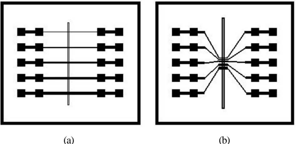
2.2 (a) Demonstration and (b) a SEM picture [20] of a sharp ditch………..…...13
2.3 (a) Demonstration and (b) a SEM picture [19] of a ramp ditch…...………..14
2.4 Steps of ditch formation [21]………....15
2.5 Bicrystal Josephson junction……….…..……..16
ix
2.7 (a) Long bridges and (b) short bridges………....18
2.8 Gradiometer……….18
2.9 dc-SQUID……….………...18
2.10 Patterning process……….………...19
2.11 Under etching (dimensions are exaggerated)………..….20
2.12 Ion Beam Etching first with 45o ….……….…..…21
2.13 The metalization holder with shield………..……..23
2.14 Diamond scribed gradiometer……….………24
2.15 Photo of a diamond scribed gradiometer……….……...24
3.1 The dewar and the modified holder……….……...28
3.2 Temperature (a) stability and (b) decrease with 1K/min [28]……….…...30
3.3 4-point probe measurement technique……….……...31
3.4 Voltage to current converter design………..……….33
3.5 The final current source design………..………35
x
3.7 The final adder design………..…..37
3.8 Complete system diagram for characterization system 1…………..…….40
3.9 Complete system diagram for characterization system 2…………..…….43
3.10 The designed dewar…….………..…….44
3.11 Thermal conductivities of common cryogenic building materials……...45
3.12 Cross-section of (a) perpendicular groove, (b) circular groove with O-Rings………...…45
3.13 Temperature vs. Time graph of the dewar while cooling………..….48
3.14 Stability. The maximum deviation from the target temperature is less than 80mK………..…49
3.15 The phase diagram [38]……….….……50
3.16 The current source design……….….….51
4.1 RCSJ (resistively capacitively shunted junction) model…………...…..54
4.2 Normalized I-V characteristics for JJ with C=0 and C=∞…...……..…..55
4.3 I-V of a dc-SQUID with steep ditch structure………....…..…57
xi
4.5 I-V of a dc-SQUID with steep ditch structure…………...…………...59
4.6 Unexpected I-V behavior of a dc-SQUID………..…….60
4.7 I-V of a dc-SQUID with steep ditch structure in Fig. 4.3 at different
temperatures……….…...61
4.8 I-V of a dc-SQUID with ramp ditch with big angle structure in Fig. 4.4 at different temperatures……….…....62
4.9 I-V of a dc-SQUID with steep ditch structure in Fig. 4.5 at different
temperatures………...…63
4.10 Unexpected I-V behavior of a dc-SQUID in Fig. 4.6 at different
CHAPTER 1. INTRODUCTION
Chapter 1
Introduction
Josephson effect and consequently Josephson junctions are the basis for superconducting electronic devices and they promise to revolutionize the electronics, as we know them today: making logic gates faster, smaller, and more efficient. This will lead to a leap in miniaturization of consumer electronics and integrated circuits. The only obstacle is the cost because they need to be cooled down to very low temperatures, thus they are only used in expensive high-speed microelectronics and quantum digital circuits. However Josephson junctions’ another property made them to be used widely, which is the sensitivity. They are the basis of SQUIDs, which are used for magnetic field detection and they have 10-14T sensitivity. They are also used as gradiometers, magnetometers, microwave detectors and very stable voltage sources.
The operation of a Josephson junction is based on its current versus voltage, I-V, characteristics. In order to have a progress in Josephson junction related world, one needs to understand the operation mechanism of Josephson junctions, and its I-V characteristics and also one needs to have some explanations for these characteristics. However, first, the I-V behavior must be observed. Thus, the focus of this thesis is to design systems that will let us observe the I-V characteristics. In addition, a simple classification of the samples that are used in this study has been done and also a number of references provided for the readers who seek more
CHAPTER 1. INTRODUCTION 2
information about the topics such as superconductivity properties and fabrication processes of samples.
In this chapter you will find some background information about superconductivity properties, brief history of them and Josephson relations that explain Josephson junction behaviors. In the second chapter, the fabrication of the Josephson junctions with ditch formation, film deposition, patterning and etching steps are explained. Then the sample preparation steps, after fabrication process until the measurement phase, for different kinds of samples such as dc-SQUIDs, gradiometers, SEJ and bicrystal junctions with bridges are explained. In the third chapter two characterization systems, which are designed and implemented, are explained step by step. In addition to cryostat and mechanical designs and considerations of both systems, also the current source, adder and the noise considerations while assembling all the parts together are explained and test results are given. Finally, our Josephson junctions’ I-V characterizations are shown, which are measured with these systems, and classified according the known models and the effects of the ditch formation on the junction characteristics are also noted. In addition, the temperature effects on I-V characteristics of the junctions are shown.
CHAPTER 1. INTRODUCTION 3
1.1 Review and Brief History of Superconductivity
At the beginning of 20th century it had been known for many years that the resistance of metals fall when cooled to lower temperatures. But it was not known what limiting value the resistance would approach, when the temperature is reduced to very close to 0 K. In 1911 Dutch physicist H. K. Onnes, 1913 Nobel Prize winner, discovered that the dc resistivity of mercury suddenly drops to zero whenever the sample is cooled below 4.2 K, the boiling point of the liquid helium, and he thought that mercury had passed into a new state and he named that state as superconductivity [1].
For a material to be a superconductor perfect conductivity is not enough, and it has to have two main properties. The first one is zero resistivity at all temperatures below a distinct temperature, which is called critical temperature, Tc. The transition from normal state to superconductor state is depicted in Fig. 1.1. In order to show the equality of dc electrical resistivity to zero many experiments have been performed. In one of these experiments, the decay of supercurrent in a solenoid was studied and the decay time of the supercurrent was found to be not less then 100,000 years [2]. The second property is perfect diamagnetism. In 1933 Meissner and Ochsenfeld noticed that the magnetic flux is expelled from the interior of the sample, which is cooled below its Tc in weak magnetic fields. The perfect diamagnetism in a superconductor is different than in a perfectly conducting material. In both cases magnetic field penetrates inside while they are in their normal states. However after transition to perfect conducting and superconducting states, the perfect conductor will still have the magnetic fields inside, trapping it, however the superconductor will expel them, as it is depicted in Fig. 1.2.
CHAPTER 1. INTRODUCTION 4 85 90 100 110 120 130 140 0.0 0.5 1.0 1.5 Normalized Resistance Temperature (Kelvin)
Figure 1.1: The transition from normal state to superconductive state on resistance versus temperature graph.
Figure1.2: Transition from Normal state to zero resistance state of perfect conductor and superconductor.
When a material goes into superconducting state, there are three constraints for staying in that state. The first one is the critical temperature, Tc, as it is mentioned above. The temperature of the material must be below Tc since the Cooper pairs are ordered below Tc and disordered above Tc, where the conduction is provided with Cooper pairs instead of normal electrons in the superconducting state.
CHAPTER 1. INTRODUCTION 5
Cooper pairs are formed by two electrons with exactly opposite spin and momentum. The Tc range of superconductors extends from 0.001 K for low -Tc materials such as Hg, Pb, Nb and NbN to 138 K for high-Tc materials such as YBCO and BiSrCaCuO. The second constraint is the critical magnetic field intensity, Hc(T), which depends on temperature. A strong magnetic field above Hc destroys the superconductivity. The third one is the critical current density, Jc. When a current is applied to a material in its superconducting state, the density of applied current must be below Jc, which depends on Hc and Tc. The superconductivity sphere in Fig. 1.3 depicts these relations clearly where superconductivity state is inside the sphere and the normal state is outside.
Figure 1.3: Superconductivity state sphere.
Many scientists tried to explain superconductivity theoretically over years and finally the first widely accepted one was BCS theory. This theory was proposed by J. Bardeen, Leon Cooper and R. Schrieffer in 1957 [3], [4]. In this theory, which was later awarded later by Nobel Prize, the superconducting electrons of the phenomenological description proved to be two electrons, Cooper pairs with opposite directions for both spin and momentum [5]. The coherence length was the size of the Cooper pair and the order parameter was proportional to the electron energy gap, which itself was proportional to the Tc. After the discovery of high-Tc superconductors, this theory was not sufficient to explain it and it is realized that this theory works only for low-Tc superconductors.
CHAPTER 1. INTRODUCTION 6
In 1962, Nobel Prize winner Brian Josephson introduced the Josephson effect, which is the basis of the promising superconducting electronics, such as SQUIDs, today. He predicted that superconducting current would tunnel through non-superconductor or insulator or weak link separating two superconducting electrodes. Thus a phase difference is produced between the superconducting electrons across the barrier, where this phase difference generates a voltage difference between the two electrodes [6], [7].
In 1986, Nobel Prize winners George Bednorz and Alex Müller, from IBM Research Laboratory in Zurich, Switzerland, produced a ceramic material by using Lanthanum, Barium, Copper and Oxygen and this material was showed to be superconducting at 30 K. This was a record for that time and opened the gates for high Tc superconductivity. The scientist had not considered ceramics as superconducting material candidates before that time and after this discovery thousands of scientists around the world started to test the different ceramic materials. Soon, in 1987, a research team from University of Alabama created a new ceramic, which showed superconductivity at 92 K. This discovery was significant because for the first time it became possible to use liquid nitrogen as a coolant. Since these materials were superconducting at significantly higher temperatures, they are referred as high temperature, high Tc, superconductors. The latest discovery, the world record, 138 K, is achieved with a ceramic that consists of the elements of mercury, thallium, barium, calcium, copper and oxygen [8]-[11].
1.2 Tunneling and Josephson Relations
Tunneling is a process that electrons can travel from one metal to another through an insulating barrier even if they don’t have enough energy to overcome or break down the insulating barrier. This process is a quantum mechanical phenomenon and quantum physics predicts that if the barrier is sufficiently thin there is a
CHAPTER 1. INTRODUCTION 7
significant probability that an electron, which impinges on the barrier, would pass from one metal to the other [8], [12].
Consider two same normal metals with an insulator in between (NIN). For tunneling of an electron in an occupied state of one side to the other, there must be an empty state available at the other side. If we also consider that electron, which tunnel, conserve energy, we can say that if there is no applied voltage across the junction, there are no empty states available under equilibrium at the other end so the electrons cannot tunnel. However if we increase the energy of one of the metals relative to the other by applying voltage, electrons can tunnel.
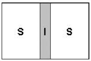
Figure 1.4: Superconductor-Insulator-Superconductor junction.
If the normal metals are replaced with superconducting ones like in Fig. 1.4, for the Cooper pair tunneling there is no need of a bias voltage. Thus no voltage would be developed for applied current to the junction, as long as it is less than some critical value, since the current is carried by Cooper pairs. In other words, there can be tunneling current (supercurrent) across the barrier at zero bias voltage. In order to show the Josephson relations let ?1 be the probability amplitude of Cooper pairs on one side and let ?2 be the amplitude on the other side [13], [14]. Actually they represent the wave functions. These wave functions start to penetrate the barrier sufficiently to couple as the thickness of the insulator in between is reduced and pairs can pass from one superconductor to the other without energy loss when the coupling energy exceeds the thermal fluctuation energy. Pair tunneling is also possible when the phases are not locked. In that case voltage needs to be applied and Cooper pairs slip relative to each other at a rate
CHAPTER 1. INTRODUCTION 8
related to the applied voltage. The time dependent wave functions can be described by 1 1 1 2 i U K t ψ ψ ψ ∂ = + ∂ h (1.1) 2 2 2 1 i U K t ψ ψ ψ ∂ = + ∂ h (1.2)
Where K represents the coupling constant and U represents the energy of a wave function for the assumption that a voltage source is applied to the superconductors or; 2 U= − eV (1.3) then, 2 1 2 ( 2 1) 2 U U U e V V eV ∆ = − = − − = − (1.4) We take the zero energy point as the midway. Then equations 1.1 and 1.2 become; 1 1 2 i eV K t ψ ψ ψ ∂ = + ∂ h (1.5) 2 2 1 i eV K t ψ ψ ψ ∂ = − + ∂ h (1.6)
We can express the wave functions as,
* 1/2 1 1 (ns1) eiθ ψ = (1.7) * 1/2 2 2 (ns2) eiθ ψ = (1.8)
CHAPTER 1. INTRODUCTION 9
Where ns stands for pair density. Then if we substitute equations 1.7 and 1.8 in to equations 1.5 and 1.6n then separating the imaginary and real parts and using
2 1
φ θ θ= − for phase difference, we get;
* 1 s n t ∂ ∂ * 1 * * 1/2 1 2 2 ( ) sin s s s n K n n t φ ∂ = ∂ h (1.9) * 2 * * 1 / 2 1 2 2 ( ) sin s s s n K n n t φ ∂ = − ∂ h (1.10) * 1 2 1/2 * 1 ( s ) cos s K n eV t n θ φ ∂ = − − ∂ h h (1.11) * 2 1 1 / 2 * 2 ( s ) cos s K n eV t n θ φ ∂ = − + ∂ h h (1.12)
The current flow from superconductor 1 to 2 is proportional to * 1 s n t ∂ ∂ , thus by using Eq.1.9 we can obtain the relation for the current density as;
sin
c
J =J φ (1.13)
Where Jc stands for the critical current density and the general expression of Jc. Jc has been derived from microscopic theory [15], and is;
( ) ( ) tanh 2 2 n ctu b G T T J A e k T π∆ ∆ = (1.14) Where A stands for the junction area and Gn stands for the tunneling conductance.
By using Eq.1.11 and Eq.1.12 the time evaluation of the difference of phase across the junction at any point is;
CHAPTER 1. INTRODUCTION 10 2 (0) e ∆ 2e V t φ ∂ = ∂ h (1.15)
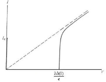
Eq.1.13 and eq.1.15 are the famous Josephson relations that express the behavior of the Cooper pairs and the I-V relation resulted from these equations depicted in Fig. 1.5 [16]-[18]. The measurements and analysis of these I-V curves is the aim of this study, which is pursued experimentally.
CHAPTER 2. FABRICATION OF JOSEPHSON JUNCTIONS AND SAMPLE PREPERATION
Chapter 2
Fabrication Of High-T
c
Josephson
Junctions And Sample Preparation
2.1 Fabrication
The samples used in this study were prepared in collaboration with ISG of Juelich Research Center, Germany. The step edge junction based samples were made using the crossing YBCO thin film across a created ditch onto the crystalline substrates creating four grain boundaries at the edges of the ditch, as explained in the following sections. The ditches on the substrates were made by ion beam etching process and super-conducting film was deposited by using pulsed laser deposition technique. They were made of typically 200nm to 300nm thick c-axis YBCO films on 1 mm thick MgO and LaAlO3 substrates. After deposition of YBCO, they were patterned by using photolithography technique. The patterns were symmetric step edge junctions, SEJ, asymmetric step edge junctions and bicrystal junctions with long and short bridges of widths from 1µm to 12µm; gradiometers with washer areas with 1.5mm diameter, loop areas of 75x75µm2 and a baseline of 1.5mm and dc-SQUIDs with 5 µm wide symmetric junctions. In order to characterize the samples we needed to follow different procedures for each of them. SEJ and bicrystal junctions were ready after cleaning with standard
CHAPTER 2. FABRICATION OF JOSEPHSON JUNCTIONS AND SAMPLE PREPERATION
12
cleaning process and contact metalization procedures. We deposited the contact pads of 500 nm thick gold layers by using shadow masks in an etch-sputter system. Then samples were connected to the system by wire contacts and silver epoxy. Gradiometers needed to be opened from the magnetic field concentrating washer areas by using diamond-scriber and lithography techniques. Then the same cleaning and metalization procedures that were used for the step-edge and the bicrystal junctions were followed. dc-SQUIDs, dc-Superconducting Quantum Interference Device, needed to be metalized gold with more precise method using lift-off technique, where the photolithography process was used, due to the very small distances between the contact pads. This is while there was also a danger during the gold deposition with sputtering technique, since the gold might diffuse under the shadow mask shorting the contacts. For attaching the sample to the cold-finger of the system we used high vacuum grease to increase the thermal conduction between the samples and the holder.
2.1.1 Ditch Formation for SEJ
One way of making a Josephson Junction, JJ, is to use a ditch on the substrate where the edge of the ditch serve as weak link for formation of JJ. These types of junctions are called step edge junctions, SEJ, as it is depicted in Fig. 2.1. Further details about the fabrication and properties of the Step Edges can be found in [19]. In order to have a Step Edge Junction, the first thing that we need on a substrate is a ditch. The used samples in this work have two kinds of ditches. One is ramped type ditch and the other one is sharp ditch as shown in Fig. 2.2 and 2.3 respectively. As explained in chapter 4, SEJs with sharp ditches has smaller critical current density, Jc, and SEJs with ramp ditches have higher critical current densities. In the following paragraph we will explain only the general ditch formation.
CHAPTER 2. FABRICATION OF JOSEPHSON JUNCTIONS AND SAMPLE PREPERATION
13
Figure 2.1: Step Edge Josephson junction.
(a)
(b)
CHAPTER 2. FABRICATION OF JOSEPHSON JUNCTIONS AND SAMPLE PREPERATION
14
(a)
(b)
Figure 2.3: (a) Demonstration and (b) a SEM picture [19] of a ramp ditch.
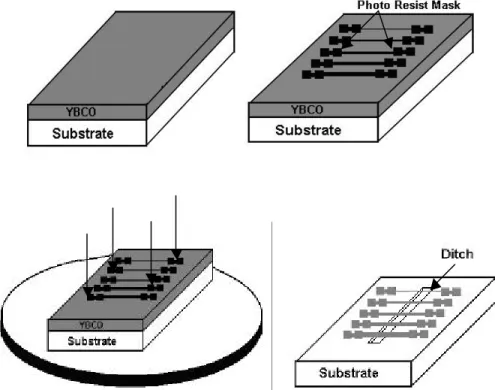
Ditch formation process is clearly depicted in Fig. 2.4, and they are created as follows. As the first step a 60nm thick e-gun evaporated gold layer is deposited on the substrate prior to the step etching process [20]. This serves as a etch resist in Ion Beam Etching (IBE) Process and it prevents roundness of edges, so clean edges are obtained at the steps. Then a layer of photo resist is coated on top of the gold layer and a photo mask (chrome mask) with a ditch structure is placed on top of the photo resist. By using standard lithography techniques the place that a ditch will be formed is exposed and all other places still remain under photo resist in the sake of protection in the etching process. Then by using Combinational Ion Beam Etching (CIBE) the ditch is formed [20]. By using different etching parameters sharp steps and ramp steps can be formed. Further details about the Lithography and the Ion Beam Etching processes can be found in sections 2.1.2 and 2.1.3,
CHAPTER 2. FABRICATION OF JOSEPHSON JUNCTIONS AND SAMPLE PREPERATION
15
respectively. Afterwards, photoresist is cleaned by using n-hexane, acetone, and propanol baths. As a last step, gold is cleaned by using iodine-potassium-iodide solution in an ultrasound bath. Finally the substrate with a ditch on it is ready to be processed further [21].
CHAPTER 2. FABRICATION OF JOSEPHSON JUNCTIONS AND SAMPLE PREPERATION
16
2.1.2 Film Deposition
The YBCO film deposition is one of the most crucial steps of the fabrication process for step edge junctions and especially for bicrystal junctions. This is because in bicrystal junctions we don’t have any ditch, and junctions are formed on the grain boundary of a specilly-manufactured substrate, where two pieces of substrate fused together with an in-plane misalignment, as shown in Fig. 2.5. Homogeneity and perfection of the film is very important. Hence, one of the best thin film deposition techniques, Pulse Laser Deposition – PLD, is used by the collaborating group in Juelich Research Center.
Figure 2.5: Bicrystal Josephson junction.
In a PLD system a pulsed laser beam of high energy is focused on the rotating target in a vacuum chamber, as shown in Fig. 2.6. The laser radiation is absorbed by a solid surface of the target, causing evaporation of the bulk YBCO materials in the chamber. Evaporants form a ‘plume’ consisting of a mixture of atoms, molecules, electrons, ions, clusters and micron-sized solid particulates. Since the collusional mean free path inside the dense plume is very short, immediately after the laser irradiation, the plume, similar to the rocket exhaust, expands away from the target with a strong forward-directed velocity distribution. The evaporated material condenses on the substrate placed opposite to the target and a thin film is formed [23]-[26]. For more information about PLD techniques you can see references [22] -[25].
CHAPTER 2. FABRICATION OF JOSEPHSON JUNCTIONS AND SAMPLE PREPERATION
17
Figure 2.6: Pulsed Laser Deposition Technique [27].
In Juelich Research Center KrF2-Excimer-Laser is used in the PLD system. Its wavelength is 248nm and pulse duration is 20nsec with 25Hz frequency. Its energy is 1 joule per pulse and creates 3-4 Joule/cm2 energy density on the target. During the deposition, the substrate is heated up to 750-800oC and oxygen is used in the vacuum chamber with pressure 0.5– 1 mbar in order to obtain a crystalline thin film. With these conditions 0.1nm YBCO per pulse can be deposited on the substrate [21]-[22].
2.1.3 Patterning
The studied samples carrying Josephson Junctions in this work have different patterns, such as symmetric step edge junctions, asymmetric step edge junctions, and bicrystal junctions with long and short bridges and various widths, as well as gradiometers and dc-SQUIDs, which are depicted in fig ures 2.7(a), 2.7(b), 2.8 and 2.9 respectively. Even though their designs are different, the technique used to pattern them is the same. They are patterned using standard photolithography procedures with either ion beam etching process, or wet (acid based) etching process.
CHAPTER 2. FABRICATION OF JOSEPHSON JUNCTIONS AND SAMPLE PREPERATION
18
(a) (b) Figure 2.7: (a) Long bridges and (b) short bridges.
Figure 2.8: Gradiometer
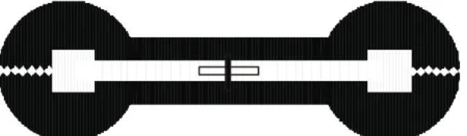
Figure 2.9: dc-SQUID
The first step in the photolithography procedure is to put a thin layer of photoresist on top of the sample. For this purpose sample is put onto spinner and after putting couple of drops of photoresist on it, it is spun with 4000rpm 40 seconds. After this procedure the thickness of the photoresist is around 1.4µm. Then it is soft baked, by drying for 5 minutes at 90oC. However the thickness of the photoresist at the edges and at the corners might be thicker than the normal
CHAPTER 2. FABRICATION OF JOSEPHSON JUNCTIONS AND SAMPLE PREPERATION
19
because of the surface stresses during spinning. Hence, the edge cleaning technique is used to remove these extra photoresist from corners and edges. Afterwards the sample is ready to be put under the mask aligner. A chrome mask with the desired pattern is put on top of the photoresist layer. Then a mercury vapor lamp whose UV radiating power is 7mW/cm2 with a wavelength of 365nm is turned on for 5 seconds. The places under chrome surface remain unexposed and clear; however the places under the transparent parts of the chrome mask get exposed to the UV-Light and at these places a photochemical destruction of carbon chains starts. Then the sample is dipped into the developer solution and the UV-Light exposed photoresist is cleared completely. Afterwards the sample is blow-dried until no more developer on top of the sample remains. At the end the structure on the chrome mask is developed on the substrate [21], [27]. The complete process is depicted in Fig. 2.10. The structure can be long or short bridges with contact places or a gradiometer structure or dc-SQUID structure.
CHAPTER 2. FABRICATION OF JOSEPHSON JUNCTIONS AND SAMPLE PREPERATION
20
2.1.4 Etching
As a last step of fabrication, thin film on the substrate is etched in such a way that the structure that we want will remain and YBCO coating at all other places is cleared or etched away.
Two ways of etching are used in our samples. One is wet etching process in which acid based chemical solutions are used to etch away the YBCO. This is the technique that is being used in our laboratory at Bilkent. The other one is the dry etching process; in which accelerated ions are used to etch away the YBCO thin film. This technique is called Ion Beam Etching, IBE, and it is used during the fabrication process of our samples in Juelich Research Center.
In wet etching process, we use 0.75% H3PO4 acid diluted with DI water [28]. We put our samples in this solution for 30 to 60 seconds. Then we wash it with DI water and blow-dried with nitrogen gas. As a last step photoresist on top of the YBCO film is cleared in an ultrasound Acetone bath. Then the sample is cleaned in an ultrasound Propanol bath and blow-dried again. The problem with this technique is, it does not work so well for feature sizes smaller than 3µm due to the under etching, as shown in Fig. 2.11.
1mm 200nm
1.5umI
Figure 2.11: Under etching (dimensions are exaggerated).
In Ion Beam Etching process, Argon cations that are accelerated with energies of 250-500eV toward the sample are used. The sample is fastened to a plate that is made of copper and in order to ensure optimal heat conductivity the surface of the plate is coated with titanium and even high vacuum grease is used between the
CHAPTER 2. FABRICATION OF JOSEPHSON JUNCTIONS AND SAMPLE PREPERATION
21
sample and the plate. The position of this plate, which is 45o, to get the optimum etching during ion bombardment, is shown in the following figure, Fig.2.12. Heat conductivity is crucial in IBE process. This is because when the sample is overheated it may cause out-diffusion of the oxygen from YBCO and polymerization of photoresist so it does not go away in an Acetone bath. Because of this, during the etching process the sample is cooled down to -10 to -15oC. Another method to make the cooling possible is, to work by 20 seconds intervals. System is on for 20 seconds and it is off for the next 20 seconds in order to let the sample cool. System checks the termination point of the etching process by the help of Secondary Ion Mass of Spectrometry (SIMS) [21].
Substrate
Holder
Argon Ions
Figure 2.12: Ion Beam Etching with 45o holder position.
2.2 Sample Preparation
After the completion of the fabrication processes, the devices are ready to be used. However in order to characterize them, further work on them was needed. Each type of the used samples in this work needed different types of procedures as explained in the following sections.
CHAPTER 2. FABRICATION OF JOSEPHSON JUNCTIONS AND SAMPLE PREPERATION
22
2.2.1 Preparation of SEJ and Bicrystal Junctions Based
Devices for Junction Characterization
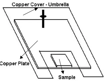
Symmetric and asymmetric step edge junctions and bicrystal junctions with long and short bridges were the ones that needed least preparation effort for the characterization. The only process needed was cleaning and the contact metalization for wire contacts. For cleaning we used first Acetone bath in a low power ultrasound for 2 minutes then Propanol bath in a low power ultrasound for 20 minutes and at the end blow-dried them. For the contact metalization we prepared a copper shadow mask by using standard PCB printing techniques. By using the prepared mask and Denton Vacuum Desk II etch-sputter unit, we first etched the contact pads of the samples for approximately 5nm and coated them with 500nm thick gold layer. The etching part was necessary to ensure the removal of all unwanted materials and a clean interface on the contact pads in order to make direct contacts to the YBCO film. During these processes, over heating was again a crucial point to be taken cared of, like in the Ion Beam Etching processes. In order to prevent over heating we put our samples on a copper plate and in order to ensure the optimal heat conduction the surface of the plate is gold coated and we put high vacuum silicon grease in between the sample and the plate. We also put a copper cover, which stands over the plate, like an umbrella and it has an empty place as big as the sample itself, so that it covers all other places and prevents the plasma from reaching and heating the unnecessary places as shown in Fig. 2.13. Another method we used to prevent the heating was to work with interrupts. We turned on the system for 15 seconds and turned it off for the next 15 seconds. This way we assured that the samples were kept cooled enough to prevent the degradation of the junctions. After this step, the samples were ready to be connected to the system. We used silver epoxy for the wire contacts and we chose our wires as thin as possible to decrease the thermal conduction via wires as much as possible. The above procedures resulted in desired contact resistances in the range of a few ohms.
CHAPTER 2. FABRICATION OF JOSEPHSON JUNCTIONS AND SAMPLE PREPERATION
23
Figure 2.13: The metalization holder with shield.
Also for some of the very sensitive samples we made direct contacts to the YBCO. This was done by using non-magnetic chip-carriers and making wire bounds from each YBCO contact pad to the chip carrier contact-pins. Then we connected chip carrier to our system by soldering, resulting again contact resistances in the range of a few ohms.
2.2.2 Preparation of Gradiometers for Junction
Characterization
Preparation of Gradiometers for the characterization of its junctions was difficult. The main problem was the closed magnetic field concentrating washer areas where the first step was to open them. We used two techniques for opening the SQUID washer areas. The first one was to use a diamond-scriber. By using backlight and magnifiers the YBCO film was scratched from the squares that are in the middle of the washer areas to the edges of the patterns, which is depicted in Fig. 2.14 and Fig. 2.15. The crucial point in this method was to prevent the
micro-CHAPTER 2. FABRICATION OF JOSEPHSON JUNCTIONS AND SAMPLE PREPERATION
24
cracks on the film and stresses on the junctions. Since YBCO has a ceramic structure, one little crack on it can spread all over the film, and it can also reach the junction area, where the cracks themselves can behave like junctions. Thus, the scratches were made with only one movement and with the least stress possible. After opening the washer area the above standard cleaning procedure was repeated to make them ready for the contact metalization. In the cleaning process first we cleaned the places that would be gold coated with n-Hexane by using Q-tip. Then we put our gradiometers into low powered ultrasound Acetone bath for 2 minutes and low powered ultrasound Propanol bath for 20 minutes and then taking them out followed by blow -drying. For metalization part we prepared a shadow mask for the gradiometers and used the same procedure that is explained in section 2.2.1. In order to connect the gradiometers to our system we used silver epoxy as explained in section 2.2.1.
Figure 2.14: Diamond scribed gradiometer.
Figure 2.15: Photo of a diamond scribed gradiometer.
The second method was to use the photolithography technique. The procedure that we have used in our lab is a little bit different than the procedure that is used
CHAPTER 2. FABRICATION OF JOSEPHSON JUNCTIONS AND SAMPLE PREPERATION
25
in Juelich Research Center. We needed to use a transparency mask instead of chrome one. Nevertheless the photolithography technique that we used was the same standard technique with different recipe, such as the photoresist dropped gradiometer was spun for 40 seconds with 6000 rpm, followed by the soft baking process for 3 minutes at 90oC. Then it was exposed with UV-Light, which has a 0.25mW/cm2 power, for 140 seconds and at the end it was put into developer solution for 45 seconds and blow-dried. Afterwards we used the same wet etching technique and same photoresist cleaning procedures that are explained in section 2.1.4. The metalization part was again the same as explained in section 2.2.1.
2.2.3 Preparation of DC-SQUIDS for Junction
Characterization
The only thing we needed to do with dc-SQUIDs, which is depicted in Fig. 2.9, was the contact metalization. For cleaning we followed the same procedures where for metalization we could not use the shadow mask and sputter system. This was because the contact areas were small and the distance between the contact pads were too small. In order to use our sputter system there should be at least 0.5mm distance between the contact pads. Otherwise gold will diffuse underneath the shadow mask during the deposition covering the isolating area, between the contacts, where it may short the pads. Because of this reason we used lift-off process. We used our lithography system for this purpose and followed the same procedures until the YBCO etching part. We did not need to repeat the etching part because we already had the appropriate YBCO structure. We covered all the places with photoresist and only left the contact areas open. Then we followed our same metalization procedure explained before without the involvement of any shadow mask. In this approach, we covered all over the sample with gold. Then we put it into low powered ultrasound Acetone bath for 60 seconds. Hence, the places that were covered with photoresist were washed away from gold and the
CHAPTER 2. FABRICATION OF JOSEPHSON JUNCTIONS AND SAMPLE PREPERATION
26
places that were not covered with photoresist remained with gold on top. The main advantage with this technique is that we can go down to micron accuracy.
CHAPTER 3. CHARACTERIZATION SYSTEMS
Chapter 3
Characterization Systems
3.1 Characterization System 1
The main goal of this study was to build an automated Josephson junction characterization system. Such a system would let to measure the current versus voltage, I-V, relation and also the dynamic resistance of the junctions, Rdynamic, dV/dI, while holding the temperature at the desired levels. The system would also allow the measurement of the resistance versus temperature relations when required. The first built characterization system consists of Janis VPF-475 liquid nitrogen based dewar, a computer controlled current source, a DSP lock-in amplifier for measuring the Rdynamic and as a signal source for modulating the current, an adder to add the dc voltage coming from data acquisition card, DAC (PCI-6024E) to the sin wave coming from the lock-in, DAC as a voltage source and for reading the measurements, a voltage preamplifier and a current preamplifier for amplifying the incoming signals, and a GPIB card (IEEE-488) for connecting all the units together and automating the operation of the system.
CHAPTER 3. CHARACTERIZATION SYSTEMS 28
3.1.1 The Cryostat and Mechanical Modifications
Figure 3.1: The dewar and the modified holder.
The first thing needed was to modify the dewar for the considered measurements, which is shown in Fig. 3.1. The outer part of the dewar was vacuumed which served as an isolation part between the outside, 300K, and the liquid nitrogen, 77.3K. The desired vacuum was reached down to 3-millitorr using a rotary vacuum pump, which can reach down to 0.45-millitorr. The vacuum level was measured with a Yellow Jacket M69075 thermocouple vacuum gauge. The dewar could take 250ml liquid nitrogen and with 3-millitorr outer vacuum level we could make measurements for up to 2 hours in the temperature stability levels that we wanted. However we couldn’t use this time effectively at the beginning because there were only 8 pins on the original holder, which allowed us to make contacts only for 2 devices on a sample at the same time. This is because we need 4 connections for a measurement since we were using four-point probe configuration technique, which is generally used to decrease the contact resistance effects on the measurements as it is depicted in Fig. 3.3. Then the system was heated, opened, and the contacts were done to other 2 devices. It took 3 measurements to complete the characterization of a sample that had 6 devices on it. Thus 2 more holes were drilled on the holder and by choosing one common
CHAPTER 3. CHARACTERIZATION SYSTEMS 29
ground pin 3 devices could be connected at the same time. This way it took only 2 measurements to complete the characterization of a sample. After changing the number of pins the wirings were also needed a change. We twisted each positive and negative couple of wires with each other and then we twisted the couples. These wires were taken to the outside by using feed-through and with shielded wires. We did not separate twists until they reached very close to the devices where they should be connected.
The temperature of the sample was measured by a Pt-500 temperature sensor, which has a linear temperature dependent resistance within the liquid nitrogen and room temperatures range. The sensor was calibrated by measuring its resistance at room temperature and at the liquid nitrogen temperature, followed by finding a linear relation between the temperature and the resistance. The resistance of the sensor was measured again with 4-point probe configuration by applying 100µA bias current from Agilent 3401A digital multimeter in order to prevent self-heating caused by the Joule self-heating. Since the aim was to read the temperature of the sample by using Pt-500, the sensor had to be as close as possible to the sample. In the first try the sensor was put side by side with the sample and then we tried to put it right under it. However the problems with these solutions were the temperature gradient between the sample and the sensor. This concern is because of the distance and in between materials between them. In order to solve this problem a groove was drilled in the holder and the thickness of the material was decreased in between. Then the sensor was mounted in that groove, right under the sample where there was also high vacuum silicon grease in between to increase the heat conduction. Other change we did on the holder was to put a heater on it. The dewar had its own heater at the beginning but it was far away from the sample, because of this we could not get the temperature stability that was desired. Thus we made a heater by using metal film surface mount resistances, which was powered by HP6628A DC power supply, and placed it 1cm away from the sample. The temperature could be controlled up to 150K with a maximum power of 5 W. The temperature control with a less than 20mK deviation was achieved by
CHAPTER 3. CHARACTERIZATION SYSTEMS 30
using these hardware configurations and PID controller software shown in Fig. 3.2(a). All these changes were the same with the ones that had been done for the bolometer measurements [28]. 0 2 4 6 8 10 12 90.56 90.57 90.58 90.59 90.60 90.61 90.62 90.63 90.64 Temperature (Kelvin) Time (Min) (a) 0 1 2 3 4 5 6 7 8 9 88 90 92 94 96 4.20 4.25 4.30 4.35 4.40 4.45 91.50 91.55 91.60 91.65 91.70 91.75 Actual Temperature Target Temperature Y =95.97032-0.99755 X Temperature (Kelvin) Time (Min) T (K) Time (min) (b)
CHAPTER 3. CHARACTERIZATION SYSTEMS 31
Figure 3.3: 4-point probe measurement technique
3.1.2 The Current Source
The major point in junction measurements is a reliable voltagecontrolled low -noise load-independent current source. These characteristics for the current source is very essential since any sudden jump in current value can burn a device and any load dependency may result in wrong measurements. We used DAC as a voltage source, the output voltage of which is changeable from –5V to 5V with 5mV steps. This resolution added another limitation to the current source. We tried many different designs; one was based on LM134 current sources and another one was based on three-transistor current source model by using LM3086. None of them satisfied stability criteria and load independency criteria. Then we moved on to the design that is depicted in Fig. 3.4, which was purely voltage-to-current converter. If we solve this circuit [29],
We can write, i1 = i2 (3.1) or 1 1 1 3 Vin V V Vo R R − = − (3.2) from above we obtain,
CHAPTER 3. CHARACTERIZATION SYSTEMS 32 1 1 3 1 1 3 1 Vin Vo R V R R R = + − (3.3) We can also write,
i3 = iL + i4 (3.4) or, 4 2 L L L Vo V V V R RL R − = + (3.5) from which we get;
4 4 1 2 L L R R Vo V R R = + + (3.6) By equating the equations 3.3 and 3.6 we get,
4 4 1 1 1 3 1 2 1 3 1 L L R R Vin V R V R R R R R + + = + − (3.7) We designed the circuit such that
4 3 2 1 R R R = R (3.8) Then 4 3 1 L L R R V Vin R R = − (3.9)
and finally we get
2 L Vin i R = − (3.10)
As we see from the equation 3.10, the circuitry behaved like a voltage-to-current converter; input voltage, Vin, is converted into the load current, iL, which is independent of RL.
CHAPTER 3. CHARACTERIZATION SYSTEMS 33
Figure 3.4: Voltage to current converter desig n.
In this configuration the stability and reliability of the current source was good where a low noise metallic 100O resistance between junction and the ground was used to monitor the current. A current source based on this design was constructed with specs that maximum current was 100µA and steps were 100nA while using low noise metal film resistances. The current source was mounted on a PCB, which was printed by using standard PCB printing techniques in order to reduce the noise, and we put it in a metal box and used two 12V batteries as voltage supplies and twisted wires and low noise connectors for connections. The circuit ground was independent of the chassis and the chassis was connected to the earth; this way chassis itself behaved like a shield. The circuitry and the batteries were also shielded with another earth grounded conductive layer. The main caution was to protect the junction; because of this, the junction was shorted by using a switch. Hence when turning the power on, the junction remained shorted and protected from spike currents. We checked the current value from monitor and then by turning on the second switch we gave the current to the junction. This
CHAPTER 3. CHARACTERIZATION SYSTEMS 34
configuration seemed working well, at the beginning, however after burning a device we realized that we needed to work on it further. When we tested the current source we saw that while turning the second switch, which was shorting the junction, on and off current jumps occurred at certain frequencies. In order to prevent these high frequency current jumps from reaching to the junction, we simply added a capacitor and a resistance to the current source, as it is seen in Fig. 3.5. This way any unexpected voltage or current jump coming from the op-amp or switches would be blocked by R2 and C1 low -pass filter configuration. There was already a resistance there and by simply adding a capacitor to that point we got a low pass filter faced to the junction. At the same point Rx and C1 and also R4 and C1 form low pass filters, which blocked any sudden voltage changes and prevented them to feed-back to the op-amp and create a big current jump. Also we chose Rx big, around 10kO, this way even if a spike reaches to Rx it would compensate the jump before reaching to the junction since junction’s resistance is around couple of 10s of ohms. Then we also changed the technique for the current monitoring. We removed that 100O monitor resistance and instead of that we connected SR550 low noise current preamplifier in between. Current preamplifier was connected to the system in series and converted the current that it sensed to the voltage at the output. Thanks to its filters and low noise mode, which allowing the readings clearly, where we read the output of it by DAC. The main advantage with this monitoring technique was we didn’t need to count on the stability of the current source, anymore, and we could read each data point’s current value separately.
After optimizing this current source, we used same principles to built 5 different current sources in the same box and we controlled them by a switch. The ranges were changing within ±100µA, ±500µA, ±1mA, ±3mA and ±7mA for various ranges with minimum steps of 100n, 500n, 1µA, 3µA and 7µA, respectively.
CHAPTER 3. CHARACTERIZATION SYSTEMS 35
Figure 3.5: The final current source design.
3.1.3 The Adder
In addition to I-V measurement we also aimed to measure the dynamic resistance of the junctions. For this purpose we needed to modulate the current and we did this by using 122Hz sine wave. We could apply the dc current and the modulated current separately. However we needed to apply them at the same time. Thus we needed an adder to sum up the dc voltage coming from DAC and sine wave coming from the lock-in amplifier to feed into current source and get a sine wave modulated dc current. As an adder we used simple adder configuration, which is shown in Fig.3.6, as a general idea.
CHAPTER 3. CHARACTERIZATION SYSTEMS 36
Figure 3.6: Simple adder design.
If we solve this circuit [29];
We can write, 3 3 2 1 1 2 R R Vo Vin Vin R R = − + (3.11) since we wanted to simply add 2 signals without any amplification, we chose
1 2 R = R =R (3.12) then,
(
)
3 1 2 R Vo Vin Vin R = − + (3.13)This design worked well but the main concern was to sum the signals as they were. Since we did not intended to amplify them or sum them wrongly, we chose R=R1=R2=R3. However there was still wrong summation danger, which comes
CHAPTER 3. CHARACTERIZATION SYSTEMS 37
from the voltage sources’ output impedances. We chose R as a 1kO and when we connect the voltage sources, since they were different, their output impedances were also different and they affected R1 and R2 differently which caused wrong summation. Thus we changed the design, as it is shown in Fig. 3.7. We used buffers at the input sides of the adder. We also wanted even the op-amps to be the same at both input sides thus we used TL082 in which op-amps are in the same package. This way whatever the resistance of the voltage sources, the summation was not affected. After we finished the circuitry construction we put the circuit in an earth grounded metal box, which behaved as a shield, as we did with the current source. We again used two 12V batteries as supplies and we made inside connections by using twisted and shielded wires. We also shielded the circuitry and batteries with another earth grounded metal layer where we also should note here that the circuit’s ground was independent of the chassis’ ground.
CHAPTER 3. CHARACTERIZATION SYSTEMS 38
3.1.4 Integrating All The Parts Together
The last thing that we needed to do in the characterization system 1 was to connect all the parts, which were tested separately, together as it is shown in Fig. 3.8. The most important point in combining the parts were to prevent any ground loops that may cause resistive coupling, which could give rise to the system noise and also to prevent any kinds of feed-back loops, which might cause unexpected voltage or current increases which might cause junction death.
The first thing was to connect the voltage inputs of the adder, where one of the inputs was coming from DAC, whose output was connected to the earth. We wanted to separate earth ground as much as possible from the circuitry ground because once it was connected from a point then it would be connected to the whole system’s circuitry since all the units’ circuitries’ grounds were combined together. Thus we used 100kO resista nce at the ground of the first input of the adder. The other input was coming from lock-in and the lock-in had two options. We could select whether we wanted to connect output of it to the earth ground or not. Despite this we put another 100kO resistance to the ground of the second input of the adder to remain in the safe side. The aim was to get rid of the noise that might come from the ground lines, where the batteries were used for this purpose. We used twisted and shielded wires to prevent any capacitiv e and inductive noise couplings as we used inside the units and we connected the shields to the earth ground only at one point. Even the units’ chassis were connected to the earth ground at one single point in order to prevent any ground loops. The adder’s output was connected to the current source’s input by using low noise connectors, which separated negative and positive lines of a connection from the shield. When we didn’t use these connectors, we used BNC connectors and we separated the shields from the lines ourselves. The current source was connected to the current pre-amplifier, which converts the current into voltage outputs and output of it was connected to the DAC that was used in a differential mode. We used the current pre-amplifier in a low noise mode in which the amplification is
CHAPTER 3. CHARACTERIZATION SYSTEMS 39
done after filtering in order to quickly ‘lift’ low-level signals above the instruments noise floor. The output of the current source went into one of the three connectors of the dewar, where each one was for a different device. Not only the shields of the wires but also the dewar itself was connected to the earth ground and it was behaving like a shield. Then the output voltage of the junction was taken again with three connectors to the out of the dewar, where each one was for a different device. One of the outputs, which belonged to the device under measurement, went to SR560 low noise voltage preamplifier. The voltage was carried again with twisted and shielded wires, this time it separated to 2 lines as a positive pole and negative pole and we used differential mode of the voltage pre-amplifier. This way we got rid of the noises that might come from the environment until the wires reach to the voltage preamplifier. We also used this device in a low noise mode with filters as we used the current preamplifier where the typical gain we used was changing from sample to sample, from 1000 to 50000. Its output was connected to DAC that is used in differential mode. The same output was also connected to lock-in, which measures the dynamic resistance and lock-in output was connected to DAC that is used again in a differential mode. We were also using lock-in as a signal source to give 122Hz 10mVpp sine wave into the system as explained above.
CHAPTER 3. CHARACTERIZATION SYSTEMS 40 Ad d e r I S o ur ce I P re -a m p V Pr e -a m p Lo ck -in M ul tim e te r G PI B B us
D
AC
Lo w R G ro un d in g Tw is te d & S hi e ld e d C ab leCHAPTER 3. CHARACTERIZATION SYSTEMS 41
3.1.5 Programming
We explained the hardware configurations of the system until now. The system was controlled by 2 programs that were written using the LabView software. The first one was the temperature control program, which mainly controlled HP6628A DC power source, Agilent 3401A and Fluke 8842A digital multimeter through a GPIB card. The program was first reading the resistance of the Pt-500 through Agilent 3410A in 4-point probe configuration and calculating the temperature by finding a linear relation between the resistance and the temperature by using the calibration points that were written by the user. The program was controlling the temperature by using a PID control unit. The cooling and the heating speeds of the system were chosen by user, and the usual speed that we used was 1K/minute as can be seen in Fig. 3.3(b). This program also provided us the R vs. T measurement. The aim was not making R vs. T measurement, however sometimes we needed to check the junctions’ superconductivity properties and because of this we used this program.
The second program was the main program that fed the current source, measured the dynamic resistance, the current, and the voltage drop on the junction. For I vs. V measurement we were doing current sweep, which was done by sweeping the input voltage of the current source. In this program user was defining start and stop values and steps of the current that will be applied and program was giving output voltages accordingly. In the input part sensitivity of DAC needed to be changed each time, because each sensitivity arrangement had its own errors and we needed to use the optimum ones each time. Thus the program checked each input value and changed the sensitivity accordingly; each taken data was written into a file and a relative graph was drawn. The program was doing these for current, voltage and the dynamic resistance readings separately, and also providing the I vs. V and the Rdynamic vs. I graphs. While all the inputs were voltages, the final data that writ ten into file was the real data, and the program was calculating the according current or resistance values by using the appropriate user
CHAPTER 3. CHARACTERIZATION SYSTEMS 42
defined constants. The time duration for each cycle was important in the measurements since the modulation frequency needed to be higher than the increment frequency of the steps. Thus at the final program, after optimizations, each cycle duration was only 0.15 seconds, which could be controlled as wanted.
CHAPTER 3. CHARACTERIZATION SYSTEMS 43
3.2 Characterization System 2
The characterization system 1 was working fine in the temperature range of 77.3K and above. However we could not observe the junctions’ typical characteristics, namely the critical current, at those temperatures. Thus we decided to reach lower temperatures where the first system was not working below 77.3K. Hence we started to build a complete new system, which can be seen in Fig 3.9.
I S ou rc e V Pr e-am p M ul tim et er G PI B B us
D
AC
Lo w R G ro un d in g Tw ist ed & S hi el d ed C ab leFigure 3.9: Complete system diagram for char
CHAPTER 3. CHARACTERIZATION SYSTEMS 44
3.2.1 The Cryostat and Mechanical Design
Figure 3.10: The designed dewar
The first thing that we needed to do was to build another dewar as shown in Fig. 3.10. While we were building the dewar we needed to take into account the thermal expansion, the thermal conductivity, and the specific heat properties of the materials that we would use. Details about thermal conductivity and expansion of the material can be found in references [30], [31]. The thermal expansion was important for us because we were building the dewar at room temperature where when the temperature is decreased down to liquid nitrogen temperature and even below, the temperature change would be more than 220K. This much temperature change could change the dimension of the materials considerably and it could cause a major stress on the parts that were bounded together by solder, by glue, or by any other means of binding techniques. The thermal conductivity of the materials was also important for us since we were trying to prevent any
CHAPTER 3. CHARACTERIZATION SYSTEMS 45
temperature escape from the dewar. Thermal conductivity plots for common cryogenic building materials are depicted in Fig. 3.11.
Figure 3.11: Thermal conductivities of common cryogenic building materials.
(a) (b)
Figure 3.12: Cross-section of (a) perpendicular groove, (b) circular groove with O-Rings.
CHAPTER 3. CHARACTERIZATION SYSTEMS 46
As shown in Fig. 3.11, Teflon has the minimum thermal conductivity, accessible, and electrically non-conductive. Thus we started to build the dewar based on a cylindrical Teflon mass, which would be the outer walls. The plan was to put liquid nitrogen in a container where this container would be surrounded by Teflon walls. The air between the teflon walls and the container would be pumped out and also the evaporated nitrogen would be pumped out in order to decrease the temperature of the liquid nitrogen. Based on this plan the first thing was to seal the cylindrical Teflon from the bottom side by using another Teflon layer. Grooves were made on both sides and o-rings that exactly fitted in the grooves were used. There were two kinds of grooves that could be used. One of them was rectangular shape groove in which the o-ring would block the air only at sides as shown in Fig. 3.12(a). The second one was round shape groove, which had the exact dimensions as the o-ring where the o-ring blocks the air at all sides as shown in Fig. 3.12(b). We chose the second one and made the groove as smooth as possible. Then we put high vacuum silicon grease around the o-ring and put it in between the surfaces and tightened it with screws. At the end also the liquid gasket was used around the sealing.
Since the area in between the liquid nitrogen container and the Teflon would behave as an insulating layer in between, we wanted this area to be as big as possible to decrease the heat transfer due to the scattering. Then we thinned the inner side of the cylinder as much as possible, but we needed to be careful because the walls should resist the vacuum level that we would apply later on. Then another Teflon layer was made with a big circler hole whose diameter was the same as the stainless steel container’s diameter. We chose stainless steel as a container because we wanted to slow down the heat transfer from the bottom to the top. The thermal conductivity property of the stainless steel is shown in Fig. 3.11. We put the container into the Teflon layer while putting Teflon bands and silicon grease in between to prevent any leakage. Also another laye r, which is aluminum, was placed between the Teflon and the steel. The inner side of the aluminum was painted black with a material that does not outgas and outer side of

![Figure 2.2: (a) Demonstration and (b) a SEM picture [20] of a sharp ditch.](https://thumb-eu.123doks.com/thumbv2/9libnet/5664378.113264/25.918.303.675.384.966/figure-demonstration-b-sem-picture-sharp-ditch.webp)
![Figure 2.3: (a) Demonstration and (b) a SEM picture [19] of a ramp ditch.](https://thumb-eu.123doks.com/thumbv2/9libnet/5664378.113264/26.918.254.723.160.627/figure-demonstration-b-sem-picture-ramp-ditch.webp)
![Figure 2.4: Steps of ditch formation [21].](https://thumb-eu.123doks.com/thumbv2/9libnet/5664378.113264/27.918.231.744.315.968/figure-steps-of-ditch-formation.webp)