DC Electrowetting of Nonaqueous Liquid Revisited by XPS
Pinar Aydogan Gokturk, Burak Ulgut, and Sefik Suzer
*
Department of Chemistry, Bilkent University, 06800 Ankara, Turkey
*
S Supporting InformationABSTRACT: Liquid poly(ethylene glycol) (molecular weight,∼600 Da) with a low vapor pressure is used as droplets in an ultrahigh-vacuum X-ray photoelectron spectrometer (XPS) chamber with traditional electrowetting on dielectric (EWOD) device geometry. We demonstrate that, using XPS data, independent of the sign of the applied voltage, the droplet expands on the substrate with the application of a nonzero voltage and contracts back when the voltage is brought back to zero. However, the main focus of the present investigation is about tracing the electrical potential developments on and around the droplet, using the shifts in the binding energy positions of the core levels representative of the liquid and/or the substrate in an noninvasive and chemically specific fashion, under imposed electrical fields, with an aim of shedding light on numerous models employed for simulating EWOD phenomenon, as well as on certain properties of liquid/solid interfaces. While the lateral resolution of XPS does not permit to interrogate the interface directly, we explicitly show that critical information can be extracted by probing both sides of the interface simultaneously under external bias in the form of potential steps or direct current. We
find that, even though no potential drop is observed at the metal-wire electrode/liquid interface, the entire potential drop develops across the liquid/solid-substrate interface, which is faster than our probe time window (∼100 ms) and is promptly complying with the applied bias until breakdown. No indication of band bending nor additional broadening can be observed in the C 1s peak of the liquid, even under electrical field strengths exceeding 107 V/m. Moreover and surprisingly, the liquid recovers within seconds after each catastrophic breakdown. All of thesefindings are new and expected to contribute significantly to a better understanding of certain physicochemical properties of liquid/solid interfaces.
■
INTRODUCTIONWettability is a key feature to describe certain properties of surfaces and is usually characterized by the contact angle between a liquid droplet and the surface. Over the decades, several chemical/physical methods have been developed to control the wettability of surfaces for various applications, such as coating, printing, etc.1,2In certain applications, active control of wettability is very crucial.2,3 Electrowetting (EW), which is usually inferred from the contact angle changes as a result of application of an external electrical potential, is one method to achieve wettability control.4,5 This process can be used to control small amounts of liquids and their movement electronically without any mechanical considerations, which has a great importance in microfluidic devices.6−8Some of the other areas benefiting from the EW phenomenon are optical lenses9,10and lab-on-a-chip systems.11−14 In the classical EW setup, where a drop of a solution is placed on top of a metal electrode and a thin wire of counter electrode is inserted into the drop from the top, the contact angle changes are small and limited because of electron transfer and eventual electrolysis of the solvent. This geometry was further improved by insertion of a dielectric layer between the liquid drop and the metal surface.15,16 This latter process is called electrowetting on dielectric (EWOD).4,17,18 In the most frequently used geometry, where the bottom conducting electrode is covered with an insulating layer with thickness t to prevent the faradic currents and other electrochemical reactions, the Young
equation combined with Lippmann’s eq 1is used to describe the contact angle in the EWOD process19
θ θ γ θ ε ε γ = + CV = + tV cos cos 1 1 2 cos 2 0 LG 2 0 0 LG 2 (1) where θ is the contact angle under the potential, θ0 is the contact angle at zero voltage, C is the capacitance, V is the external voltage,γ is the surface tension of the liquid, t is the thickness of the dielectric layer, ε and ε0 are the relative
permittivities of dielectric and vacuum, respectively. It is also common to further coat the dielectric layer with another thin hydrophobic layer (i.e., Teflon or other fluoropolymers) to increase the contact angle for better visualization of the effect.20−24Lately, instead of solid dielectric layer between the liquid droplet and underlying electrode, a new approach has
been introduced, which uses liquid-infused films as the
dielectric layer, where complete electrowetting and reprodu-cible reversibility are achieved to enable capturing transient responses optically.25 In majority of the EW experiments reported in the literature, water or aqueous salt solutions are used and the ambient medium is either air or another immiscible liquid or oil. Even though water is a useful solvent, it is not good for many applications in microfluidics due to its Received: April 22, 2018
Revised: May 31, 2018 Published: June 5, 2018
pubs.acs.org/Langmuir Cite This:Langmuir 2018, 34, 7301−7308
Downloaded via BILKENT UNIV on February 25, 2019 at 11:31:26 (UTC).
of the drop to evaporate. To overcome this shortcoming, liquids with nearly zero vapor pressure can be used. Previously, we used a similar sample configuration without the dielectric layer between the drop and metal substrate to monitor the generation of carbene species through electroreduction of imidazolium-based ionic liquids.30,31 We have also recently reported another XPS study to monitor the charge screening of an ionic liquid across the two co-planar gold electrodes on a porous polymer surface.32,33In the present study, we report on the use of poly(ethylene glycol) (PEG) with an average molecular weight of 600 Da. PEG with a small molecular weight is in its liquid form and has negligible volatility, which makes it suitable for UHV experiments. PEG is a well-studied liquid polymer that has been utilized in many applications ranging from personal care products to food industry.34 It is also biodegradable and has considerable potential in the use of droplet-based microfluidics for biological applications.35,36
XPS is a powerful tool not only for conventional chemical analysis but also for monitoring of the electrical potentials developed on surface structures, from the measured shifts in the binding energy of the representative core levels, which can deliver pivotal information related to electrical double layer (EDL) formation.37−39In our previous work mentioned above, we used such information to estimate the capacitance ratio of the top and bottom electrodes of the ionic liquid drop on the Si substrate30 or the effect of the EDL formation with both temporal and lateral resolutions across a co-planar capacitor having an ionic liquid electrolyte medium.32,33 Herein, we present an investigation, which will also focus on extraction of information related to the electrical potential developments on or around the solid/liquid interface, under imposed electrical fields for the direct current (DC) electrowetting on dielectric phenomenon. The use of PEG for XPS analysis brings an added advantage of having both carbon and oxygen atoms with a single chemical state and being devoid of ions, except for impurities. As a result, it is expected that the imposed electric field interacts predominantly with the dipoles of the liquid structure. To our knowledge, this is thefirst time that XPS is used for tapping into the EW phenomenon and we believe that ourfindings are crucial to understand and correctly model the EWOD process.
■
EXPERIMENTAL SECTIONPEG was purchased from Merck and used as received. The Si substrate used has a nominal 300 nm oxide layer, which is further coated with a hydrophobic CYTOP (Bellex International Corporation) layer of∼50 nm thickness. This hydrophobic surface now acts as the substrate on the planar electrode. PEG drop (3 μL) is placed on top of this fluoropolymer using a micropipette, and a copper wire is inserted into the drop as the counter electrode (seeFigure 1). A Thermo Fisher K-Alpha ray photoelectron spectrometer with monochromatized X-rays of 1486.6 eV is used to collect data for all measurements. Data manipulation is carried out using the Avantage software. A DataPhysics OCA is used for contact angle measurements and drop shape analysis. An external DC bias is applied using a Keithley 2400 SourceMeter to either the droplet or the Si substrate. For pulsed measurements, a Stanford Research System Model DS340 Function Generator is used.
Details of XPS data collection, charging, and/or bias-dependent shifts for both the liquid droplet and the hydrophobized substrate are given in Supporting Information (SI)Figure S1a−c.
■
RESULTSGeometrical Changes. Images of a PEG droplet under +50, +10, 0,−10, and −50 V in ambient air are shown inFigure 2. A“negative” applied potential corresponds to (−) voltage at the electrode underneath the substrate and 0 V at the inserted wire. The contact angle of the droplet on hydrophobic fluoropolymer is around 89° with no electric field. When the applied potential becomes more negative or positive, the droplet electrowets the surface and decreases its contact angle. However, the contact angle values for negative and positive biases are slightly different. This asymmetry in electrowetting response has been known and can be related to the semiconductor electrode used as one of the electrodes40 or fluoropolymers used as a dielectric for aqueous solutions. The latter was claimed to be the consequence of permanent trapping of charge carriers at thefluoropolymer surface, which increased with aging of substrates in water as well as in various nonaqueous polar liquids.41 Hence, the nonaqueous PEG on the CYTOP layer, used in this work, also exhibits an asymmetric EW response. Similar visual changes are also observable when the device is in the XPS chamber.
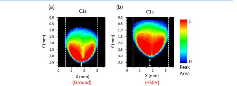
Since the substrate is coated with a hydrophobic layer, the high amplitude of the applied bias may lead to movement of the drop from its original position together with a change in its shape and contact angle. To reflect the changes that the drop undergoes, we display an aerial map of C 1s peak integrated intensity in Figure 3a, recorded in the snapshot mode of the instrument with 50 μm X-ray spot size and 50 μm step size, when both electrodes are grounded.
Due to the large number of data points acquired, the faster data gathering using the snapshot mode was preferred. However, this mode offers lower spectral resolution. It is also important to be highly cautious since carbon signal is observed on both the substrate and the droplet, together with the presence of the adventitious carbon everywhere. For that reason, we carefully select and fit the sharp PEG peak with deviations in the C 1s position smaller than 0.2 eV from its mean value of 286.4 eV all throughout (see SIfor details on data handling). This intensity map of C 1s represents almost a circular shape of the drop in the beginning with some distortion because of the inserted wire electrode to the droplet, convoluted with the angled X-rays illumination geometry. In any case, it is possible to estimate the base area of the drop as
∼5.8 mm2. Figure 3b shows the map under +50 V bias.
Contrary to the grounded case, there is only one single C 1s Figure 1.Schematic of EWOD device. The bottom plate has a silicon wafer with 300 nm thick oxide layer and CYTOP coating. The counter electrode is a copper wire. The PEG droplet is between the plate and wire.
Figure 2.DC voltage dependence of contact angle and shape of PEG droplet. The voltage increased from 0 to 50 V and then back to 0 V and decreased from 0 to−50 V gradually.
Figure 3.C 1s map of the PEG drop in vacuum when (a) grounded and (b) under + 50 V bias.
Figure 4.Intensity alterations in the O 1s and F 1s regions due to changes in the shape and contact angle of the drop, recorded at a point on the drop/substrate interface, under periodic applications of 0 and−50 V.
peak, which is again at 286.4 eV, because application of the bias causes the carbon peaks stemming from the substrate to move out of the range to∼50 eV higher binding energy values (see
Figure S1c). At the same time and under the bias, the drop expands, distorts further, and also moves about 0.5 mm without breaking its electrical connection. Basal area of the drop after +50 V is estimated as∼6.7 mm2, which corresponds to 17%
increase in the initial area. If we keep the volume of the drop unchanged and simply calculate the effect of this 17% increase in the base area to the contact angle, then it corresponds to ∼12° change from the initial contact angle value (computa-tional details are given in theSI). This change is smaller than the measurements outside the chamber, which might be related to the contact angle saturation phenomenon, since the drop had been exposed to several voltage cycles before these particular data were acquired.42
Dynamic expansion and contraction of the drop can also be monitored by sequential gathering of O 1s (representing the drop) and F 1s (representing the rigid substrate) regions in the snapshot mode on a point at the drop/substrate interface under successive −50 and 0 V DC excitations. Figure 4 shows the temporal changes of intensities of the O 1s and F 1s peaks. The cycle begins with application of a−50 V, at which the F 1s peak appears around 650 eV, the drop expands, and the intensity of
the O 1s peak (at ∼532 eV) increases. We note that the
measured position of the F 1s differs about 10 eV from the expected value of 640 eV (690−50), due to (positive) charging nature of the hydrophobic substrate, under X-ray exposure. When the voltage applied is 0 V, the F 1s goes back to its original binding energy position and disappears from the
observation window completely and the intensity of O 1s peak decreases but does not disappear completely, since it is well-established that liquids leave wedgelike residues on the substrate.1,4,43 These periodic alterations are surprisingly fast, in orders of tens of milliseconds, much faster than the slow (>10 s) ion movements and/or charging events, which will be demonstrated and discussed further in the proceeding sections. Potential Developments. To improve the spectral quality, we have also acquired data in the scanning mode, which is inherently slower and hence allows analysis of only few selected points on the sample or along a selected line (line scans). Accordingly, while an external DC bias (+50, 0, and−50 V) is applied to the Si electrode, we acquired C 1s XPS data on a selected line starting from the substrate surface, going toward the middle of the drop, as depicted in Figure 5. Similar information can also be obtained from the O 1s peak of the liquid (not shown).
When both electrodes are grounded, the C 1s region exhibits one narrow (full width at half-maximum = 1.2± 0.2 eV) peak at 286.4 eV representing the liquid and another broad feature
with multiple components (C−F, C−F2, C−O−F, etc.)
representing the substrate. When 50 V bias is applied, the binding energy position of thefirst peak (of the liquid) displays no shift and no broadening with neither the amplitude nor the polarity of the bias, whereas the second broad peak (of the substrate) shifts with the bias. Physical movement of the drop with the bias is also observed due to changes in the lateral position of the drop/substrate interface. Upon reversing the connection, mirroring potential developments are observed, where the C 1s peak shifts promptly with the bias and the F 1s Figure 5.(a−c) C 1s spectra recorded at different applied biases along the line shown in the inset. The lateral position of the liquid/substrate interface, determined by the region where both C 1s features overlap, also moves with the bias.
experiences no significant shifts, as given inFigure S5of the SI. Naturally, the source electrode and the substrate experience binding energy shifts equal to or less (due to charging) than the applied potential depending on its electrical conductivity, while no corresponding shifts are observed on the drop, since it is in contact with the grounded wire electrode.
The crucial information lies on the electrical properties of the medium between the two electrodes. In one of our previous publications on a pristine graphene medium, we reported on measurements of the C 1s peak position and showed that it exhibited a smooth and linear binding energy shift across the two electrodes behaving like a simple resistive strip. We also
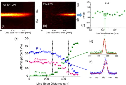
showed that after introducing defects and cracks in the graphene layer on purpose, these linear deviations were lost locally.44In a more recent work, we used ionic liquids as the medium between two electrodes and, in this case, the F 1s signal of the ionic liquid exhibited a constant and nonvarying shift across the electrodes. Moreover, the measured amplitude of the shift was dependent on the nature and geometry of electrodes. For instance, with a symmetrical co-planar geometry, where the device had two similar gold electrodes, the binding energy shift was only half of the imposed potential, since the applied potential drop was shared equally by the two equivalent electrode/electrolyte interfaces, which was attributed Figure 6.Line scan spectra of (a) F 1s and (b) C 1s regions, recorded under +100 V bias and with 30μm spot size and 20 μm step size, along a line into the drop. (c) Variations in the width of the C 1s peak. (d) Atomic percentages and the representative (e) C 1s and (f) F 1s spectra at the designated point.
Figure 7.Time-resolved C 1s spectra recorded (a) under 10 single-quantum well excitation (>12 spectra/s). (b, c) Same spectra recorded after breaking of the +10 and−10 V bias (open circuit), respectively (∼1 spectrum/s).
the liquid (PEG), only the substrate complies with the applied −50 and + 50 V biases and shifts and the peak of the drop maintains its binding energy position as in the grounded form. In the present geometry, one would have expected that EDL formation at the electrode/liquid interface plays crucial roles in dictating the electrical potential developments, but the surprising finding is that the entire potential drop (full bias) materializes only at the substrate/liquid interface. Thisfinding is further supported by the mirrored measurements when the +100 V bias is applied to the liquid drop through the wire electrode, as shown inFigure 6. More data are given inFigure S2of the SI.
As can be evidenced from the figure, the measured binding energy with +100 V bias is 386.3± 0.1 eV along the line. Using this simultaneous measurement of the potential developments on the substrate and the liquid of a 30μm spot on the liquid/ substrate interface, one can observe that electricalfields larger than 107V/m are sustained, without any sign of band bending
or spectral deterioration.
Another surprising finding is related to the unexpectedly large region, where the F 1s and C 1s signals of the substrate overlap for ∼200 μm, covering more than six spot sizes (30 μm) of the X-rays used, possibly indicating that a very thin layer of the liquid creeps from the drop toward the substrate, but still in electrical contact with the drop. This may be related to previously reported wedgelike extension of the liquids on the substrate,43,45 which by itself is very interesting, since we continue measuring the same potential difference in the region. However, this point lies outside the scope of the present study, but will be the subject of a future work.
Temporal variations using time-resolved measurements also show that development of this full potential drop is faster than 100 ms, as shown in Figure 7. In the same figure, spectra recorded under open-circuit potential (OCP) conditions are also given, where now, as opposed to the fast potential rise, the potential drop takes much longer time, in orders of several hundreds of seconds. This experiment indicates that the mechanism that develops the potential at the interface is resilient and does not quickly self-discharge. In conventional electrochemical investigations on batteries or solar cells, OCP measurements reveal pertinent information related to the local state of charge, surface photovoltage kinetics, etc.46,47However, the same information cannot be directly extracted from our measurements, since very different processes contribute to the decay of the accumulated charges on the liquid drop, such as the magnitude of the imposed potential, charge accumulation caused by X-rays, photoelectron emission, etc., and we will not discuss the issues any further here.
Measurements leading to extracting the potential develop-ments on and around the liquid drop can be carried out even under very severe conditions, as long as the integrity of the vacuum system is preserved, as demonstrated inFigure 8, for the case of dielectric breakdown. Here, the surprisingfinding is that even though the liquid distorts severely and various mechanical movements are visually observable, as shown in the video clip given in theSI, the developed voltage exhibits only
small deviations and recovers within seconds. The dielectric breakdown is an important phenomenon limiting the applicability of the EW process, and a huge scientific effort has been devoted to understand and circumvent it.48−52 Therefore, chemically specific information derivable using our approach can provide a completely fresh investigation perspective.
■
DISCUSSIONThe outcome of the measurements made in the previous section brings out several important facts all related to the electrical potential developments on the surface of the liquid drop, which is: (i) fast (<0.1 s rise time), (ii) uniform on the entire drop, (iii) robust (>102s decay time), and (iv) to some extent, resilient even after a hard breakdown, accompanied with a large increase in the current passing (see theSI). Moreover, under very significant electric fields approaching the dielectric breakdown strength, no sign of band bending is evidenced spectroscopically, although a significant current jump can be recorded, as shown inFigure S6bin the SI.
The fast nature of the potential developments points to an associated electronic process50,51although the liquid purposely chosen is predominantly a dipolar one and the uniformity is in stark contrast to the frequently used electrical circuit model for EWOD simulations, reproduced in Scheme 1. As depicted in the scheme, which is similar to that shown inFigure 1, when a Figure 8.C 1s spectra recorded at +20 V increments until the onset of the breakdown at +120 V and then at∼1 min intervals, but still under +120 V. We note that the drop recovers and returns to the fully applied bias within minutes.
Scheme 1. Equivalent-Circuit Model for the EWOD Process,
−100 V bias is applied through the Si electrode while the liquid is grounded, the applied potential should drop across the silicon oxide dielectric layer (∼300 nm) and the top hydrophobic CYTOP layer (∼50 nm, seeFigure S6a) differently and should be inversely proportional to their capacitances.
The capacitances can be estimated using the relationship C = ε0·ε/t, where t is the thickness and ε is the dielectric constant,
which are 2.1 and 3.9 for the hydrophobic and silicon oxide layers, respectively.48,49 This simple back-of-the-envelope calculation gives the capacitance ratio (Ch/Cd) as 3.7 and
dictates that a very significant voltage drop (>20 V) ought to be measured on the surface of the hydrophobic substrate. In fact, the hydrophobic substrate does display small noncomplying binding energy shifts due to its charging nature, as discussed earlier and also shown in Figure S2b, but these shifts are completely negligible compared to the values obtained using the equivalent circuit model, which calls for serious amendment in the current understanding of certain properties of the liquid/ dielectric interfaces. On the other hand, simple calculation using dielectric strengths correctly predicts the onset of the breakdown voltage to be about 120 V (details of the estimation are given in theSI).
■
CONCLUSIONSWe have investigated a dielectric liquid drop in vacuum for the first time, using two important resources of XPS, mainly its ability to yield: (i) quantitative chemical information and (ii) local information related to potential developments upon imposing electrical fields. Our investigation produced several newfindings pertaining to important chemical/physical proper-ties of the liquid. Accordingly, movement of the liquid drop under the influence of applied electrical fields, and accompany-ing geometrical changes associated, can be recorded and followed over its chemical constituents by XPS, which, in turn, can be related to the contact angle changes at the liquid/solid interface. The potential developments on both the liquid drop and the dielectric substrate can also be followed all the way up to the breakdown of the substrate and even beyond. The liquid complies very quickly (<0.1 s) and adopts the full voltage imposed uniformly on the entire surface of the drop. By simultaneous measurements of the potential developments on the substrate and the liquid on the liquid/substrate interface, one can observe that electrical fields larger than 107V/m are sustained, without any sign of band bending or spectral
deterioration. These findings can impact on many of the
physicochemical aspects of liquid, interface, and electro-chemical sciences. The main objective of the present study has been an introduction of the novel experimental method-ology, and it naturally calls for further experimental and theoretical studies to follow up the many issues only
superficially touched upon in the present study. Our
experimental strategy is simple and can be easily adopted by all XPS instruments, lab-based or otherwise.
■
ASSOCIATED CONTENT*
S Supporting InformationThe Supporting Information is available free of charge on the
ACS Publications website at DOI: 10.1021/acs.lang-muir.8b01314.
Details of data gathering modes used; additional data and estimation of the geometrical changes in the shape of the drop using the XPS data; and images of the liquid drop in
ambient air under bias up to the breakdown and beyond (PDF)
■
AUTHOR INFORMATION Corresponding Author*E-mail:[email protected].
ORCID
Pinar Aydogan Gokturk:0000-0001-8269-8884
Burak Ulgut:0000-0002-4402-0033
Sefik Suzer: 0000-0002-5866-2600
Author Contributions
The manuscript was written through contributions of all authors. All authors have given approval to thefinal version of the manuscript.
Notes
The authors declare no competingfinancial interest.
■
ACKNOWLEDGMENTSThis study was partially supported by the Scientific and Technological Research Council of Turkey (TUBITAK) Grant No. 215Z534.
■
REFERENCES(1) de Gennes, P. G. Wetting: statics and dynamics. Rev. Mod. Phys. 1985, 57, 827−863.
(2) Adamson, A. W.; Gast, A. P. Physical Chemistry of Surfaces; Wiley: New York, 1997.
(3) Xin, B.; Hao, H. Reversibly switchable wettability. Chem. Soc. Rev. 2010, 39, 769−782.
(4) Jones, T. B. On the Relationship of Dielectrophoresis and Electrowetting. Langmuir 2002, 18, 4437−4443.
(5) Mugele, F.; Baret, J.-C. Electrowetting: from basics to applications. J. Phys.: Condens. Matter 2005, 17, R705−R774.
(6) Chatterjee, D.; Hetayothin, B.; Wheeler, A. R.; King, D. J.; Garrell, R. L. Droplet-based microfluidics with nonaqueous solvents and solutions. Lab Chip 2006, 6, 199−206.
(7) Hong, J.; Kim, Y. K.; Won, D.-J.; Kim, J.; Lee, S. J. Three-dimensional digital microfluidic manipulation of droplets in oil medium. Sci. Rep. 2015, 5, No. 10685.
(8) Pollack, M. G.; Fair, R. B.; Shenderov, A. D. Electrowetting-based actuation of liquid droplets for microfluidic applications. Appl. Phys. Lett. 2000, 77, 1725−1726.
(9) Kuiper, S.; Hendriks, B. H. W. Variable-focus liquid lens for miniature cameras. Appl. Phys. Lett. 2004, 85, 1128−1130.
(10) Berge, B.; Peseux, J. Variable focal lens controlled by an external voltage: An application of electrowetting. Eur. Phys. J. E 2000, 3, 159− 163.
(11) Srinivasan, V.; Pamula, V. K.; Fair, R. B. An integrated digital microfluidic lab-on-a-chip for clinical diagnostics on human physio-logical fluids. Lab Chip 2004, 4, 310−315.
(12) Gong, J.; Kim, C.-J. C. All-electronic droplet generation on-chip with real-time feedback control for EWOD digitial microfluidics. Lab Chip 2008, 8, 898−906.
(13) Ren, H.; Fair, R. B.; Pollack, M. G. Automated on-chip droplet dispensing with volume control by electro-wetting actuation and capacitance metering. Sens. Actuators, B 2004, 98, 319−327.
(14) Sadeghi, S.; Ding, H.; Shah, G. J.; Chen, S.; Keng, P. Y.; Kim, C.-J. C.; van Dam, R. M. On Chip Droplet Characterization: A Practical, High-Sensitivity Measurement of Droplet Impedance in Digital Microfluidics. Anal. Chem. 2012, 84, 1915−1923.
(15) Moon, H.; Cho, S. K.; Garrell, R. L.; Kim, C.-J. C. Low voltage electrowetting-on-dielectric. J. Appl. Phys. 2002, 92, 4080−4087.
(16) Seyrat, E.; Hayes, R. A. Amorphous fluoropolymers as insulators for reversible low-voltage electrowetting. J. Appl. Phys. 2001, 90, 1383−1386.
Modulation of Ionic Liquids in Oil and under AC Electric Field. ChemPhysChem 2010, 11, 2327−2331.
(21) Paneru, M.; Priest, C.; Sedev, R.; Ralston, J. Static and Dynamic Electrowetting of an Ionic Liquid in a Solid/Liquid/Liquid System. J. Am. Chem. Soc. 2010, 132, 8301−8308.
(22) Schneemilch, M.; Welters, W. J. J.; Hayes, R. A.; Ralston, J. Electrically Induced Changes in Dynamic Wettability. Langmuir 2000, 16, 2924−2927.
(23) Welters, W. J. J.; Fokkink, L. G. J. Fast Electrically Switchable Capillary Effects. Langmuir 1998, 14, 1535−1538.
(24) Eaker, C. B.; Dickey, M. D. Liquid metal actuation by electrical control of interfacial tension. Appl. Phys. Rev. 2016, 3, No. 031103.
(25) Hao, C.; Liu, Y.; Chen, X.; He, Y.; Li, Q.; Li, K. Y.; Wang, Z. Electrowetting on liquid-infused film (EWOLF): Complete reversi-bility and controlled droplet oscillation suppression for fast optical imaging. Sci. Rep. 2014, 4, No. 6846.
(26) Nanayakkara, Y. S.; Perera, S.; Bindiganavale, S.; Wanigasekara, E.; Moon, H.; Armstrong, D. W. The Effect of AC Frequency on the Electrowetting Behavior of Ionic Liquids. Anal. Chem. 2010, 82, 3146− 3154.
(27) Paneru, M.; Priest, C.; Sedev, R.; Ralston, J. Electrowetting of Aqueous Solutions of Ionic Liquid in Solid−Liquid−Liquid Systems. J. Phys. Chem. C 2010, 114, 8383−8388.
(28) Millefiorini, S.; Tkaczyk, A. H.; Sedev, R.; Efthimiadis, J.; Ralston, J. Electrowetting of Ionic Liquids. J. Am. Chem. Soc. 2006, 128, 3098−3101.
(29) Chevalliot, S.; Heikenfeld, J.; Clapp, L.; Milarcik, A.; Vilner, S. Analysis of Nonaqueous Electrowetting Fluids for Displays. J. Disp. Technol. 2011, 7, 649−656.
(30) Gokturk, P. A.; Salzner, U.; Nyulászi, L.; Ulgut, B.; Kocabas, C.; Suzer, S. XPS-evidence for in-situ electrochemically-generated carbene formation. Electrochim. Acta 2017, 234, 37−42.
(31) Gokturk, P. A.; Donmez, S. E.; Ulgut, B.; Turkmen, Y. E.; Suzer, S. Optical and XPS evidence for the electrochemical generation of an N-heterocyclic carbene and its CS2 adduct from the ionic liquid [bmim][PF6]. New J. Chem. 2017, 41, 10299−10304.
(32) Camci, M. T.; Aydogan, P.; Ulgut, B.; Kocabas, C.; Suzer, S. XPS enables visualization of electrode potential screening in an ionic liquid medium with temporal- and lateral-resolution. Phys. Chem. Chem. Phys. 2016, 18, 28434−28440.
(33) Camci, M. T.; Ulgut, B.; Kocabas, C.; Suzer, S. In-Situ XPS Monitoring and Characterization of E3lectrochemically Prepared Au Nanoparticles in an Ionic Liquid. ACS Omega 2017, 2, 478−486.
(34) Chen, J.; Spear, S. K.; Huddleston, J. G.; Rogers, R. D. Polyethylene glycol and solutions of polyethylene glycol as green reaction media. Green Chem. 2005, 7, 64−82.
(35) Knop, K.; Hoogenboom, R.; Fischer, D.; Schubert, U. S. Poly(ethylene glycol) in Drug Delivery: Pros and Cons as Well as Potential Alternatives. Angew. Chem., Int. Ed, 2010, 49, 6288−6308.
(36) Aschenbrenner, O.; Supasitmongkol, S.; Taylor, M.; Styring, P. Measurement of vapour pressures of ionic liquids and other low vapour pressure solvents. Green Chem. 2009, 11, 1217−1221.
(37) Brown, M. A.; Redondo, A. B.; Sterrer, M.; Winter, B.; Pacchioni, G.; Abbas, Z.; van Bokhoven, J. A. Measure of Surface Potential at the Aqueous-Oxide Nanoparticle Interface by XPS from a Liquid Microjet. Nano Lett. 2013, 13, 5403−5407.
(38) Brown, M. A.; Abbas, Z.; Kleibert, A.; Green, R. G.; Goel, A.; May, S.; Squires, T. M. Determination of Surface Potential and Electrical Double-Layer Structure at the Aqueous Electrolyte-Nano-particle Interface. Phys. Rev. X 2016, 6, No. 011007.
of fluoropolymer-water interfaces probed by electrowetting. Faraday Discuss. 2017, 199, 29−47.
(42) Drygiannakis, A. I.; Papathanasiou, A. G.; Boudouvis, A. G. On the Connection between Dielectric Breakdown Strength, Trapping of Charge, and Contact Angle Saturation in Electrowetting. Langmuir 2009, 25, 147−152.
(43) Yeo, L. Y.; Chang, H.-C. Static And Spontaneous Electro-wetting. Mod. Phys. Lett. B 2005, 19, 549−569.
(44) Gokturk, P. A.; Kakenov, N.; Kocabas, C.; Suzer, S. Raman and X-Ray photoelectron spectroscopic studies of graphene devices for identification of doping. Appl. Surf. Sci. 2017, 425, 1130−1137.
(45) Shin, J. H.; Kim, G. H.; Kim, I.; Jeon, H.; An, T.; Lim, G. Ionic liquid flow along the carbon nanotube with DC electric field. Sci. Rep. 2015, 5, No. 11799.
(46) O’Regan, B. C.; Bakker, K.; Kroeze, J.; Smit, H.; Sommeling, P.; Durrant, J. R. Measuring Charge Transport from Transient Photo-voltage Rise Times. A New Tool To Investigate Electron Transport in Nanoparticle Films. J. Phys. Chem. B 2006, 110, 17155−17160.
(47) Piller, S.; Perrin, M.; Jossen, A. Methods for state-of-charge determination and their applications. J. Power Sources 2001, 96, 113− 120.
(48) Berry, S.; Kedzierski, J.; Abedian, B. Irreversible Electrowetting on Thin Fluoropolymer Films. Langmuir 2007, 23, 12429−12435.
(49) Liu, H.; Dharmatilleke, S.; Maurya, D. K.; Tay, A. A. O. Dielectric materials for electrowetting-on-dielectric actuation. Micro-syst. Technol. 2009, 16, 449−460.
(50) Mibus, M.; Hu, X.; Knospe, C.; Reed, M. L.; Zangari, G. Failure Modes during Low-Voltage Electrowetting. ACS Appl. Mater. Interfaces 2016, 8, 15767−15777.
(51) Mibus, M.; Zangari, G. Performance and Reliability of Electrowetting-on-Dielectric (EWOD) Systems Based on Tantalum Oxide. ACS Appl. Mater. Interfaces 2017, 9, 42278−42286.
(52) Kavousanakis, M. E.; Chamakos, N. T.; Ellinas, K.; Tserepi, A.; Gogolides, E.; Papathanasiou, A. G. How to Achieve Reversible Electrowetting on Superhydrophobic Surfaces. Langmuir 2018, 34, 4173−4179.