Charge Trapping Memory with 2.85-nm Si-Nanoparticles Embedded in HfO2
N. El-Ataba, B. B. Turgutb, A. K. Okyayb,c,d, A. Nayfeha
a
Institute Center for Microsystems – iMicro, EECS, Masdar Institute of Science and Technology Abu Dhabi, United Arab Emirates
b
UNAM-National Nanotechnology Research Center, Bilkent University, 06800 Ankara, Turkey
c
Institute of Materials Science and Nanotechnology, Bilkent University, 06800 Ankara, Turkey
d
Department of Electrical and Electronics Engineering, Bilkent University, 06800 Ankara, Turkey
In this work, the effect of embedding 2.85-nm Si-nanoparticles charge trapping layer in between double layers of high-қ Al2O3/HfO2 oxides is studied. Using high frequency (1 MHz)
C-Vgate measurements, the memory showed a large memory window
at low program/erase voltages due to the charging of the Si-nanoparticles. The analysis of the C-V characteristics shows that mixed charges are being stored in the Si-nanoparticles where electrons get stored during the program operation while holes dominate in the Si-nanoparticles during the erase operation. Moreover, the retention characteristic of the memory is studied by measuring the memory hysteresis in time. The obtained retention characteristic (35.5% charge loss in 10 years) is due to the large conduction and valence band offsets between the Si-nanoparticles and the Al2O3/HfO2 tunnel oxide. The results show that band
engineering is essential in future low-power non-volatile memory devices. In addition, the results show that Si-nanoparticles are promising in memory applications.
Silicon-nanoparticles have been extensively investigated and considered as good candidates for storage elements in next-generation low power and high density non-volatile charge trapping memory devices (1-7). However, the size of the nanoparticles greatly affects the memory performance. In fact, as the size of the nanoparticle is reduced, its bandgap, work-function, and charging energy increase, while its electron affinity and dielectric constant reduce (8-11). Earlier, we demonstrated memory devices with 2-nm Si-nanoparticles and holes storage was observed due to the small electron affinity of the nanoparticles and therefore a lack of conduction band offset between charge storage layer and tunnel oxide was obtained (12-14). In this work, 2.85-nm Si-nanoparticles are studied as the charge trapping layer of MOS memory devices with double layer Al2O3/HfO2
tunnel oxide. Mixed charging is observed due to the increased electron affinity. Electrical characterization and energy band diagram analysis of the fabricated memory devices are provided to understand the effect of the 2.85-nm Si-nanoparticles charge trapping layer on the memory performance.
The memory cells are fabricated on an n+-type (111) (Antimony doped, 15-20 mΩ-cm) Si wafer. 5-nm-thick tunnel oxide Al2O3 is deposited at 250°C in Cambridge Nanotech Savannah-100 atomic layer deposition (ALD) system. Then, 1-nm-thick HfO2
is deposited by Plasma Assisted ALD at 195°C in an Oxford FlexAL system. Next, 2.85-nm Si-nanoparticles are spin coated on the sample. Again, a 1-2.85-nm-thick HfO2 is deposited by plasma assisted ALD at 195°C. Finally, an 8-nm-thick Al2O3 blocking oxide
is deposited by ALD at 250°C. A 400-nm-thick Al layer for the gate contact is e-beam evaporated using a shadow mask with 10 µm feature size which eliminated the need for lithography steps. A cross-sectional illustration of the fabricated memory device is depicted in Figure 1.
Figure 1: Schematic cross-section of the fabricated charge trapping memory cell with 2.85-nm Si nanoparticles.
The fabricated memory devices are electrically characterized by measuring the high frequency (1 MHz) C-Vgate characteristics of the programmed and erased states. Using the Agilent B1505A Semiconductor Device Parameter Analyzer, the memory cells gate voltage was first swept from -6 V forward to 6 V then backwards. A 1.8 V threshold voltage (Vt) shift is observed. The C-V measurements are repeated at a gate sweeping
voltage of 8/-8 V and both erased and programmed states shifted outwards as shown in Figure 2 resulting in a 4.5 V memory window. This indicates that unlike smaller Si-nanoparticles (2-nm) which are found to store only holes due to the smaller electron affinity (6), 2.85-nm Si-nanoparticles in the charge trapping layer are storing mixed charges: electrons and holes, however, more charging is due to holes revealed by the greater shift of the erased state in the negative direction as shown in Figure 2.
Figure 2: Measured hysteresis behavior using the C-Vgate characteristic showing a 4.5 V Vt shift at 8/-8 V
Moreover, the Vt shift is measured at different gate sweeping voltages as sown in
Figure 3 and the charge trapping density in the Si-nanoparticles is calculated using the following equation (15-18) and found to be 2.32 ×1013 cm-3:
q V N t t ∆ × = Ct [1]
where Ct is the capacitance of the memory per unit area, ∆Vt is the Vt shift, and q is the
elementary charge.
Figure 3: Measured threshold voltage shift using the C-Vgate characteristic at different gate sweeping
voltage.
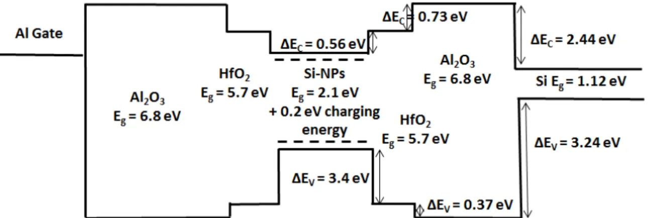
In addition, the energy band diagram of the memory with Si-nanoparticles is constructed as shown in Figure 4 using the reported electron affinities, band offsets, and band gaps of Al2O3, HfO2, and 2.85-nm Si-nanoparticles (19-32). The changes due to
quantization and coulomb charging energy of the 2.85-nm Si-nanoparticles are included. The conduction band offset between Si and tunnel oxide is smaller than the valence band offset (∆EC = 2.44 eV < ∆EV = 3.24 eV), thus the electrons tunneling probability is
expected to be higher. However, the conduction band offset between the 2.85-nm Si-nanoparticles and tunnel oxide is much smaller than the valence band offset (∆EC = 1.29
eV << ∆EV = 3.77 eV). This means that stored electrons can leak out and tunnel back to
the Si channel much easier than holes. This confirms the observed larger charging due to holes in Figure 2. Moreover, the addition of the high-dielectric constant (қ=20) HfO2
layer is expected to reduce the leakage of stored charges.
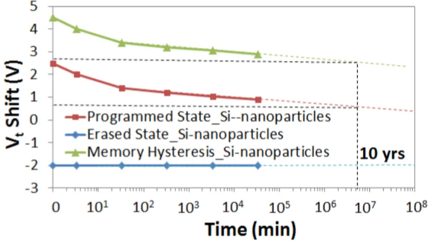
Moreover, the retention of the memory cells with Si-nanoparticles is characterized by first programming/erasing the memory at 8/-8 V and observing the change in Vt shift in time as shown in Figure 5. The memory with Si-nanoparticles showed a loss of 35.5% of the initial charge in 10 years. Also, Figure 5 shows that the measured Vt of the erased
state is almost constant in time which means that holes retention in the Si-nanoparticles after 10 years is excellent, however, the Vt of the programmed state is reducing in time
which means that electrons are leaking out at a faster rate. This can be explained from the energy band diagram plot in Figure 4 where the valence band offset between the charge trapping layer and the Al2O3 tunnel oxide is much larger than the corresponding valence
band offset (∆EC = 1.29 eV < ∆EV = 3.77 eV) which exponentially reduces the back
tunneling of holes.
Figure 5: Retention characteristic of the MOS memory with 2.85-nm Si-nanoparticles
In conclusion, 2.85-nm Si nanoparticles charge trapping layer is studied in MOS memory devices with double layer Al2O3/HfO2 tunnel oxide. The results show that a wide
memory hysteresis is obtained at low operating voltages due to charging in the Si-nanoparticles. The Si-nanoparticles are found to be storing mixed charges unlike smaller Si-nanoparticles (2-nm). Also, the good retention characteristic of such memory structure is due to the large conduction and valence band offsets between charge storage layer and tunnel oxide. The results show that such memory structures have potential in future low power non-volatile-memory devices.
Acknowledgments
This work was supported by Masdar Institute of Science and Technology, and TUBITAK Grants 111A015, 112M004, 112E052 and 113M815. A.K.O. acknowledges support from the Turkish Academy of Sciences Distinguished Young Scientist Award (TUBA GEBIP).
References
1. H. I. Hanafi, S. Tiwari, I. Khan, IEEE Trans. Electron Devices 43, 1553 - 1558 (1996)
2. O. M. Nayfeh, D. A. Antoniadis, K. Mantey, M. H. Nayfeh, Appl. Phys. Lett. 90, 153105 (2007)
3. N. El-Atab, A. Ozcan, S. Alkis, A. K. Okyay, and A. Nayfeh, Appl. Phys. Lett.
104, 013112 (2014)
4. G. Belomoin, J. Therrien, A. Smith, S. Rao, S. Chaieb, M. H. Nayfeh, Appl. Phys.
Lett. 80, 841 (2002)
5. J. J. Lee, D. K. Kwong, IEEE Elect. Dev. Lett. 52, 507 (2005)
6. O. M. Nayfeh, Ph.D dissertation, EECS, MIT, Cambridge, MA (2009)
7. N. El-Atab, A. Ozcan, S. Alkis, A. K. Okyay, and A. Nayfeh, Phys. Status Solidi
RRL 8, 629 (2014) DOI: 10.1002/pssr.201409157
8. Y. C. King, T. J. King, C. M. Hu, IEEE Trans. Electron Devices 48, 696-700 (2001)
9. J. P. Proot, C. Delerue, G. Allan, Appl. Phys. Lett. 61, 1948 (1992)
10. D. V. Melnikov, J. R. Chelikowsky J R, Physical Review B 69, 113305-113308 (2004)
11. Y. S. Park, S. W. Lee, J. S. Lee, Elec. Dev. Lett. 31, 1134-1136 (2010)
12. N. El-Atab, A. Rizk, B. Tekcan, S. Alkis, A. K. Okyay, and A. Nayfeh, Phys.
Status Solidi A 212 (2015) / DOI 10.1002/pssa.201431802
13. N. El-Atab, A. Ozcan, S. Alkis, A. K. Okyay, and A. Nayfeh, 14th IEEE
International Conference on Nanotechnology p. 505-509. DOI:
10.1109/NANO.2014.6968168 (2014)
14. A. Nayfeh, A. K. Okyay, N. El-Atab, A. Ozcan, S. Alkis,Invited, 226th ECS
Meeting Abstract no. 46, p. 2143-2143 (2014)
15. Sze SM., Ng KK. Physics of Semiconductor Devices, Third ed., JOHN WILEY & SONS, Hoboken, New Jersey (2007)
16. DJ. Griffiths Introduction to Quantum Mechanics, Second ed., Prentice Hall, Upper Saddle River, New Jersey (2004)
17. A. Nayfeh, A. K. Okyay, N. El-Atab, F. Cimen, S. Alkis, Invited, 226th ECS
Meeting Abstract no. 37, p. 1879-1879 (2014)
18. N. El-Atab et al. Appl. Phys. Lett. 104, 253106 (2014)
19. C. M. Tanner, Y. C. Perng, C. Frewin, S. E. Saddow, J. P. Chang, Appl. Phys. Lett.
91, 203510 (2007)
20. H. He, R. Orlando, M. A. Blanco, R. Pandey, E. Amzallag, I. Baraille, M. Rérat, Phys. Rev. B 79, 195123 (2006)
21. M. F. Li et al. 7th International Conference on Solid-State and Integrated Circuits
Technology, Proceedings. 1, 366 (2004)
22. L. Y. Lin, R. Puthenkovilakam, and J. P. Chang, Appl. Phys. Lett. 81, 2041 (2002) 23. R. Tsu, D. Babić, Jr. L. Ioriatti, J. Appl. Phys. 82, 1327 (1997)
24. N. Takiguchi, S. Koba, H. Tshuchiya, M. Ogawa, IEEE Trans. Electron Devices,
59, 206 (2012)
25. N. El-Atab, A. Rizk, A. K. Okyay, A. Nayfeh, AIP Advances 3, 112116 (2013) 26. N. El-Atab, F. Cimen, S. Alkis, A. K. Okyay, and A. Nayfeh, Appl. Phys. Lett.
105, 033102 (2014)
27. G. Mazzeo et al. Appl. Phys. Lett 96, 213501 (2010)
28. S. J. Choi, J. H. Han, S. Kim, D. I. Moon, M. Jang, and Y. K. Choi, 2010
Symposium on VLSI Technology Digest of Technical Papers, 111-112, (2010)
29. H. X. Wang, J. Liu, W. Bai, and D. L. Kwong, IEEE Trans. Electron Devices 51, 597–602 (2004)
30. N. El-Atab et al., AIP Advances 3, 102119 (2013) 31. S. D. Ganichev, Physical Review 61, 10361 (2000)