modification of compact TiO
2
layer by different boronic acid functionalized
self-assembled monolayers
Çisem Kırbıyık
a,b,⁎, Duygu Akın Kara
c, Koray Kara
d, Sümeyra Büyükçelebi
e, Mesude Zeliha Yiğit
f,
Mustafa Can
f, Mahmut Kuş
gaDepartment of Chemical Engineering, Konya Technical University, 42075, Turkey bDepartment of Chemical Engineering, Selcuk University, 42075, Turkey cDepartment of Physics, Mugla Sıtkı Kocman University, 48000, Turkey dDepartment of Physics, Selcuk University, 42075, Turkey
eAdvanced Technology and Application Center, Selcuk University, 42075, Turkey fDepartment of Engineering Sciences, Izmir Katip Celebi University, 35620, Turkey gInstıtute of Energy Technologies, Gebze Technical University, Turkey
A R T I C L E I N F O
Keywords:
Self-assembled monolayer Bulk heterojunction Polymer solar cells Compact TiO2
A B S T R A C T
In this study, we demonstrate the use of a series of boronic acid functionalized self-assembled monolayers (SAMs) to improve photovoltaic device performance P3HT and PCBM based solar cells. The SAMs treated compact TiO2(c-TiO2) layer was utilized as an electron transport layer for inverted polymer solar cells (PSCs)
with a configuration of FTO/c-TiO2/SAM/P3HT:PCBM/PEDOT:PSS/Ag. The modified with
3,4,5-methox-yphenylboronic acid (3-OMe) SAM shows the best improving due to the enhancement of Jscand Vocin device,
which leads to a 26% improvement (2.8%) over non-modified device (2.2%). The enhancement in the modified devices is achieved by SAM modification reducing recombination of charges and improving charge selectivity. These results prove that the surface and electrical properties of compact TiO2(c-TiO2) layer can be easily tuned
as well as the upper layer morphology can be controlled by SAM modification.
1. Introduction
Polymer solar cells (PSCs) have received significant attention as an alternative photovoltaic application due to their unique advantages, in-cluding light-weight materials, inexpensive fabrication, flexibility and ap-plicability to roll-to-roll processing techniques [1,2]. After the introduction of bulk heterojunction (BHJ) structure, PSCs have shown a remarkable improvement in photovoltaic performance [3]. Typically, BHJ structure is a photoactive blend of donor and acceptor materials sandwiched between two electrodes to compose a bicontinuous interpenetrating network for an efficient dissociation of the exciton [4,5]. The most extensively studied BHJ blend is the combination of poly(3-hexylthiophene) (P3HT) and (6,6)-phenyl-C61-butyric acid methyl ester (PCBM) [6]. Until today, the power conversion efficiencies (PCEs) of PSCs have been reported by over 13% in the comprehensive research in new organic semiconductors, device struc-ture and interface modification techniques [7–9].
BHJ structures have basically two groups: conventional and in-verted structure. The conventional structure is composed of a hole
transport layer (HTL) and photoactive blend sandwiched between an anode and a low work function (LWF) metal, whereas the inverted structure is composed of an electron transport layer (ETL) and photo-active blend sandwiched between a cathode and high work function (HWF) metal [10]. In comparison to conventional structure, inverted structure is relatively more stable in air due to the presence of HWF metals (such as Ag and Au) as top electrodes and this offers the possi-bility for using of simple fabrication techniques such as lamination or printing [11–13]. Although the inverted structure has higher photo-current and flexible design, the PCEs of most inverted PSCs reported to date are behind that of conventional structure [1,14,15]. In inverted structure, the surface of metal oxides utilizing as ETL with photoactive blend have hydroxyl groups, which cause to charge recombination and trapping at the interface [16]. Besides, PSCs performance is highly sensitive to morphology of BHJ layer and un-optimized morphology may also leads to various energy conversion losses [17]. In order to overcome these problems, interfacial contact and surface morphology of active layer needs to be improved [18]. One approach is to use a
self-https://doi.org/10.1016/j.apsusc.2019.01.268
Received 6 December 2018; Received in revised form 21 January 2019; Accepted 28 January 2019
⁎Corresponding author at: Department of Chemical Engineering, Konya Technical University, 42075, Turkey. E-mail address:[email protected](Ç. Kırbıyık).
Available online 29 January 2019
0169-4332/ © 2019 Elsevier B.V. All rights reserved.
assembled monolayer (SAM) to modify the interface between the or-ganic and inoror-ganic metal oxide layer [19]. SAMs can be used to reduce resistance across the inorganic metal oxide interface and to improve charge transfer properties and energy level alignment at interface [20]. Additionally, SAMs can be utilized as a template to control the upper layer morphology leading to produce high-performance organic elec-tronics [21]. Even though, the use of SAMs has been widely studied for the modification of interfaces of dye-sensitized solar cells and organic light-emitting diodes, there are limited studies for the BHJ solar cell interfaces [22–24].
TiO2 is one of the most studied material serving as ETL or hole blocking layer (HBL) in inverted PSCs structure due to its exceptional optoelectronic properties, stability and transparency [25]. Therefore, the compact TiO2(c-TiO2) was chosen as ETL. However, the controlling of sufficient and homogeneous formation of TiO2blocking layer is difficult
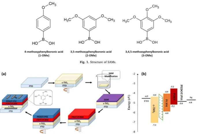
and the surface obtained has cracks or pinholes after thermal treating at high temperature [26]. This limits the electron extraction, which leads to poor photovoltaic performance. SAMs can also help to improve the quality of TiO2blocking layer. In this paper, we attempted to modify the interface of c-TiO2and photoactive layer by using three boronic acid functionalized SAMs and to enhance the photovoltaic characteristics of inverted solar cells. The molecular structures of 1-OMe (4-methoxyphenylboronic acid), 2-OMe (3,5-methoxyphenylboronic acid) and 3-OMe (3,4,5-methox-yphenylboronic acid) SAMs are shown inFig. 1. These molecules can help to cover in the cracks on surface of c-TiO2thin film owing to their small structure and to tune charge transfer properties of ETL [27]. In our work previously reported, these SAMs have been used for modification of c-TiO2 surface in methyl ammonium lead iodide perovskite solar cells and here, we attempted to understand the role of them in PSCs. Modification of c-TiO2using SAMs with permanent dipole moment can be used for tuning
Fig. 2. (a) Schematic diagram of modification procedure and (b) and the energy level diagram of the PSCs.
Fig. 3. Water contact angle measurements on c-TiO2non-modified and c-TiO2modified with 1-OMe, 2-OMe and 3-OMe SAMs surfaces (from left to right).
Table 1
The calculated values of water contact angle, work function change and average roughness differences between unmodified and modified c-TiO2surfaces
with different SAMs.
Surface Contact angle(0) Average roughness, R
a(nm) ΔΦ Values (eV)
c-TiO2/FTO 34.1 16.1 –
1-OMe/c-TiO2/FTO 64.3 16.0 0.173
2-OMe/c-TiO2/FTO 63.6 14.3 0.235
the work function. When the work function of c-TiO2matches well with the conduction band of PCBM, a good ohmic contact can be established for enhanced solar cell performance. Therefore, the effects of various para-substituents on the SAM were investigated on the photovoltaic perfor-mance of PSCs. The results showed that our solar cells with 1-OMe, 2-OMe and 3-OMe SAMs gave significant PCEs of 2.26%, 2.34 and 2.76%, re-spectively, which are superior to that of non-modified device. With this study, we report an easy and efficient method to improve photovoltaic characteristics for future application.
2. Experimental 2.1. Device preparation
The FTO (fluorine-doped tin oxide) substrates (1.5 cm × 1.5 cm) were cleaned in an ultrasonic bath with Hellmanex soap solution di-luted by deionized (DI) water, acetone, isopropanol and DI water for 15 min successively, and then dried with nitrogen gun, followed by oxygen plasma treating for 5 min. To form a thin c-TiO2 layer, the
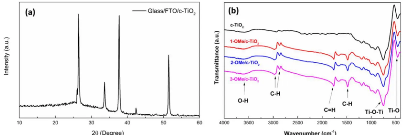
Fig. 4. Characterizations of c-TiO2surfaces by XRD and FTIR techniques. (a) XRD pattern and (b) FTIR spectra.
solution of acetyl acetone (Sigma-Aldrich, 99.5%) and titanium (IV) isopropoxide (Sigma-Aldrich, 99.9%) in absolute ethanol was spin coated at 1500 rpm for 20 s and 2000 rpm for 20 s, followed by sin-tering at 450 °C for 30 min.
The SAM modification method showed inFig. 2(a) is essentially the same as described previously [28]. To prepare the active layer solution, P3HT (Sigma-Aldrich) and PCBM (Lumtec) were dissolved in chlor-obenzene at the ratio of 1.0:0.6 wt% with a concentration of 40 mg/mL and mixed at 70 °C for 24 h. After filtering through a 0.22 μm poly-tetrafluoroethylene (PTFE) syringe filter, the blend solution was spin coated at 1000 rpm for 1 min, followed by annealing at 160 °C for 10 min. Subsequently, poly(3,4-ethylene dioxythiophene):poly(styrene sulfonate) solution (PEDOT:PSS, Clevios PVP AI 4083) was spin coated onto the blend layer at 2000 rpm for 1 min, followed by annealing at 110 °C for 10 min. Finally, 100 nm of Ag was deposited by thermal evaporation on top of the PEDOT:PSS layer.
2.2. Film and device characterization
The c-TiO2surfaces were characterized on the substrates modified with SAMs and non-modified by taking multiple contact angle mea-surements (Kruss Easy Drop). The morphological analyses of as-pre-pared films are completed by atomic force microscope (AFM, NT-MDT INTEGRA Solaris) in “tapping” mode. Kelvin Probe force microscopy (KFM) was used to analysis the surface potential variations of c-TiO2 surfaces after modification. The optical absorbance spectra of c-TiO2 surfaces were obtained over the wavelength range 300–800 nm using Biochrom Libra S22 ultraviolet-visible (UV–vis) absorption spectro-meter. A contact profilometer (NanoMap-500LS 3D Stylus) was used to determine prepared film thicknesses. The structure of c-TiO2layer was
examined by X-ray diffraction (XRD, Bruker D8 Advance). The surface chemistry properties of c-TiO2surfaces were examined by using FTIR spectrophotometer (Bruker Vertex 70) in wavenumber ranges of 400–4000 cm−1. X-ray photoelectron spectroscopy (XPS) was per-formed with SPECS EA 300 using an aluminium anode to identify the surface chemical composition of 3-OMe modified c-TiO2layer. Surface chemistry was determined using a standard peak deconvolution method. The current-voltage (J-V) characteristics of solar cells were measured under N2 in glovebox using a Keithley 2400 source mea-surement unit and glove-box integrated ATLAS solar simulator used as AM1, 5 light sources.
3. Results and discussion 3.1. Structure and morphology
The device configuration [FTO/c-TiO2 (90 nm)/P3HT:PCBM (200 nm)/PEDOT:PSS (50 nm)/Ag (100 nm)] is shown inFig. 2(a). In order to check the successful attachment of the SAMs and coverage on surfaces, the hydrophobicity of the modified surfaces was analyzed by measuring the contact angle (CA) values. Optical images of water drop and average contact angles calculated on the various SAM modified surfaces are given in Fig. 3 andTable 1, respectively. On the non-modified surface, the contact angle was 340 showing a hydrophilic surface. After modifying the surface with SAMs, the results show an increase to 650in contact angle indicating the more hydrophobic sur-face. The difference of contact angle data between non-modified and modified surfaces is related to the surface energy.Fig. 4(a) shows the corresponding XRD spectrum of spin-coated c-TiO2layer on FTO glass after sintering in air at 450 °C. A set of the strong peak at 26.40, 33.60,
37.70, 42.30and 51.40reveal that the c-TiO
2layer is a tetragonal rutile structure (JCPDS card no. 21–1276). The FTIR absorption spectra of c-TiO2films modified with SAMs are shown inFig. 4(b). The broad band around 3500 cm−1observed indicates the OeH stretching vibration of absorbed molecular water. The all spectra show two strong peaks around 450 cm−1 and 750 cm−1 corresponds to TieO and Ti-O-Ti bonding, respectively [29]. The peaks at 2985, 2869 and 1475 cm−1 corresponds to CeH bonding [30] and the peak around 1765 cm−1
corresponds to C]O bonding of SAMs [31]. The survey and high-re-solution XPS scan spectra of the 3-OMe/c-TiO2surface reveals char-acteristic peaks from the c-TiO2surface itself and from the C 1 s, B 1 s (a weak peak at 191.9 eV) [32] and O 1 s core levels of the attached or-ganic molecule (Fig. 5). InFig. 5(b), the C 1 s spectrum can be fitted to two characteristics peaks. The peaks at 286.1 and 284.2 eV can be as-signed to CeO bonds [33] and C]C bonds [34], respectively. InFig. 5 (c), the Ti 2p spectrum can be fitted to two peaks at 457.5 and 463.2 eV, which can be assigned to the Ti 2p3/2and Ti 2p1/2peaks [35]. The O 1 s spectrum of 3-OMe/c-TiO2surface is given inFig. 5(d), which is fitted to two peaks. The peaks at 529.1eV and 531.7eV are attributed to lattice oxygen, TiO2and –OH from the absorbed H2O on TiO2surface [36–38], respectively.
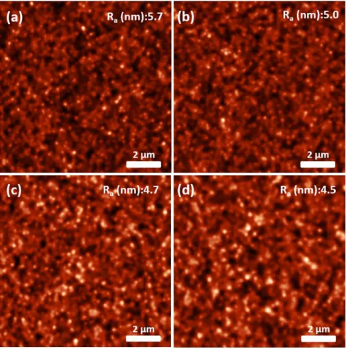
The morphology of c-TiO2films modified with SAMs was analyzed by AFM measurements. Average roughness (Ra) of c-TiO2surfaces are given inTable 1. Panels a, b, c and d ofFig. 6show the representative AFM surface morphology images of c-TiO2surfaces. As seen inTable 1, there is no significant difference between the measured Raof modified and non-modified c-TiO2surfaces. Additionally, the representative AFM surface morphology images of P3HT:PCBM layers onto (a) non-mod-ified and (b) 1-OMe, (c) 2-OMe, and (d) 3-OMe modnon-mod-ified c-TiO2layer is compared inFig. 7. As seen, the modification through any of the SAMs onto c-TiO2results reduced roughness of P3HT:PCBM surface. It can be said that the morphology of P3HT:PCBM layer seems to be influenced by SAMs. As well known, the morphology is a result of the grain size of P3HT and PCBM [39]. To quantify the statistical distribution of grain size of P3HT:PCBM thin films, the AFM images given in Fig. 7 (10 μm × 10 μm) was analyzed by using an image processing software equipped with AFM. The grain size values calculated of the films were
Fig. 7. AFM images of P3HT:PCBM layer on top of the c-TiO2surfaces. (a) Non-modified, (b) 1-OMe modified, (c) 2-OMe modified and (d) 3-OMe modified
(10 μm × 10 μm).
32.79 nm, 30.87 nm, 24.41 nm and 21.45 nm for non-modified, 1-OMe modified, 2-OMe modified and 3-OMe modified surfaces, respectively. The grain size of P3HT and PCBM onto 3-OMe/c-TiO2 layer is the smallest in comparison to those of other surfaces, which is consistent with the Ravalues. This shows that the presence of SAMs effects the upper layer growth and morphology. The reduced roughness of the photoactive layer is desirable for effective transportation of charge-carriers.
To our knowledge, the work function (Φ) of surfaces can be tuned by using dipoles of SAMs [40]. After SAM modification, the work function changing (ΔΦ) of c-TiO2were obtained by Eq.(1)as given in below;
= SAM c TiO2 (1)
As given inTable 1, the shift in the work function increases with the increasing the number of OCH3units due to different dipole moment of
SAMs [41]. The terminal functional group is the most important para-meter directing work function due to the dipole moment. Generally, the increase in ΔΦ leads to increase the Vocand Jscbecause of the increased electric field at short circuit [42]. The variation in Jscbetween PSCs modified with different SAMs could be attributed to the variation of charge-pair generation because of electric field dependent exciton dis-sociation probability [43]. To investigate the SAMs modifying effect on the optical properties of c-TiO2layer, UV–vis absorption spectra were recorded (Fig. 8). It can be said that SAM modification shows little influence on the light absorption of c-TiO2layer. There are many re-ports that TiO2in rutile structure has direct and indirect band gap [44]. In order to determine the band gap values of c-TiO2surfaces, UV–vis absorption data were fitted to equation of indirect and direct bandgap. Fig. 9(a) and (b) show the plot of (hνα)1/2vs. photon energy (hν) and the plot of (hνα)2vs. (hν) for indirect and direct band gap, respectively, where α is the optical absorption coefficient. The values of band gaps are determined by extrapolating to the X-axis intercept. As shown in Table 2, the indirect and direct band gaps value of non-modified c-TiO2 layer is ∼3.54 eV and 3.78 eV, respectively. The indirect band gap values can be tuned to ∼3.37, 3.40, and 3.44 eV for modified c-TiO2 with 3-OMe, 2-OMe and, 1-OMe respectively, whereas direct band gap can be tuned to ∼3.61, 3.64, and 3.65 eV for modified c-TiO2with 3-OMe, 2-OMe and 1-3-OMe, respectively. Lower indirect band gap can enhance the electron injection and transport of c-TiO2layer [45]. Ad-ditionally, the decrease of the direct band gap of modified c-TiO2than non-modified c-TiO2is beneficial in increasing the absorption, thus, the photocurrent of the solar cell [46]. These results are in agreement with the findings of the work function changing and resistance results. It is
Fig. 9. (a) Indirect band gap and (b) direct band gap estimation from UV–Vis absorption spectra. Table 2
Direct and indirect bandgap transitions for non-modified and modified c-TiO2
surfaces.
Surface Bandgap (eV)
Indirect Direct
c-TiO2/FTO 3.54 3.78
1-OMe/c-TiO2/FTO 3.44 3.65
2-OMe/c-TiO2/FTO 3.40 3.64
3-OMe/c-TiO2/FTO 3.37 3.62
clear that the both the indirect and direct band gap values decrease with the increasing number of bonded methoxy functional groups of SAM molecules.
3.2. Photovoltaic performance
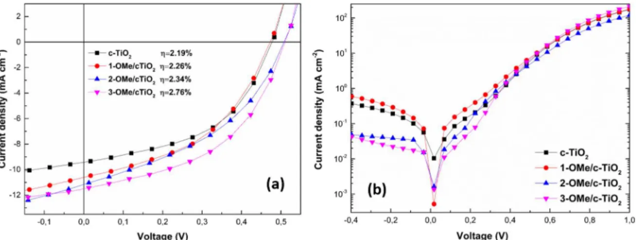
In order to improve the performance of the inverted PSC, we used the different boronic acid functionalized SAM molecules on the top of c-TiO2layer as a modification layer.Fig. 10(a) shows the corresponding current density vs. voltage (J-V) characteristics and the corresponding photovoltaic parameters of the best devices from both forward scan (FS) and reverse scan (RS) directions are listed inTable 3. Compared with the non-modified device, open circuit voltage (Voc) and short circuit current (Jsc) values were both enhanced, after the deposition of any of SAM. The control device (non-modified) shows a PCE value of ∼2.2% with a Voc of 0.478 V, a Jscof 9.4 mA cm−2 and a fill factor (FF) of 48.65%, which is a comparable result to the PCE reported in literature [47,48]. The best device (modified with 3-OMe) shows a PCE value of ∼2.8% with a Voc of 0.512 V, a Jsc of 11.5 mA cm−2 and a FF of 46.87%. The Jscvalues show an enhancement from 9.4 mA cm−2to 11.5 mA cm−2in the order of J
sc, 3-OMe> Jsc, 2-OMe> Jsc, 1-OMe> Jsc, non-modified. This enhancement can be attributed to the improving of interface electron transfer, as illustrated inFig. 2(b), by reducing the trap states on the c-TiO2layer [49]. The SAM modified devices show slightly improved Vocvalues, while the FF values remain nearly similar to that of non-modified device. The changing of Vocvalues could be explained by the change in the work function of c-TiO2layer [50]. This is in agreement with the changing of ΔΦ values.
The series and parallel resistances can be utilized to determine the solar cell performance. The series and parallel resistances were ob-tained from J-V curves and the values obob-tained are shown inTable 3. The modified devices with SAMs show advancements in series re-sistance (Rs) from 22 Ω to 12 Ω. It can be seen that the SAM molecules reduce the device series resistance by surface trap state passivation [27]. As seen in dark J-V curves inFig. 10(b), the diode performances of SAMs modified devices show similar advancement. In case of using SAMs, the devices show an increase in parallel resistance (Rp). Higher Rp originates from the reducing the loss of the back charge re-combination and the trapping of the carriers, leading to improve in device performance [51]. In addition, higher Rp leads to increased photocurrent density. This proves that the morphological and electrical properties of PSCs can be easily improved by modifying c-TiO2layer with SAMs. The J-V characteristics measured in the dark was identified
using Shockley-Read-Hall equation, Eq. (2), to understand the me-chanisms governing charge transport and recombination [52].
=
J J exp qV
n k T 1
o
B (2)
where J is the current density, V is the applied voltage, Jois the reverse saturation current density, n is the ideality factor, q is the electron charge, kBBoltzmann's constant, and T is temperature. The n and Jo values are extracted from the slope and intercept of the dark J-V characteristics on a logarithmic plot, respectively. The n and Jovalues extracted are listedTable 4. It can be clearly seen that the Jovalues decrease markedly owing to the decreasing back charge recombination after modification. Similarly, the devices modified with SAMs show a decrease in n values, which is in agreement with the findings of the resistance calculation. A series of boronic acid derivative SAMs with various dipoles can be used to reduction of the contact resistance be-tween c-TiO2layer and P3HT:PCBM layers.
4. Conclusions
In summary, we showed that the presence of SAM interface layer between the inorganic TiO2and P3HT:PCBM layer can enhance the PCE of PSCs. Depending on the nature of SAMs, the charge transport and contact properties at interlayer can simply be tuned as well as the upper layer growth and morphology can be effected. As seen, the best device with 3-OMe SAM modification (resulted a PCE of ~3%) shows a 26% improvement over non-modified device, thanks to improved values of Vocand Jsc. The improved device performance (the modified by any of SAM) is due to the reduction of back charge recombination at the in-terface, passivation of surface trap state on c-TiO2layer and mediation of better charge transfer. In this study, the results present a simple and useful method to improve the photovoltaic parameters of inverted PSCs fabricated. Additionally, the obtained results would be helpful for high-performance PSCs for future applications.
References
[1] A.M.S. Salem, S.M. El-Sheikh, F.A. Harraz, S. Ebrahim, M. Soliman, H.S. Hafez, I.A. Ibrahim, M.S.A. Abdel-Mottaleb, Inverted polymer solar cell based on MEH-PPV/PC61BM coupled with ZnO nanoparticles as electron transport layer, Appl. Surf. Sci. 425 (2017) 156–163.
[2] V.-H. Tran, R. Khan, I.-H. Lee, S.-H. Lee, Low-temperature solution-processed ionic liquid modified SnO2 as an excellent electron transport layer for inverted organic solar cells, Sol. Energy Mater. Sol. Cells 179 (2018) 260–269.
[3] C. Liang, Y. Wang, D. Li, X. Ji, F. Zhang, Z. He, Modeling and simulation of bulk heterojunction polymer solar cells, Sol. Energy Mater. Sol. Cells 127 (2014) 67–86. [4] L. Lu, T. Zheng, Q. Wu, A.M. Schneider, D. Zhao, L. Yu, Recent advances in bulk
heterojunction polymer solar cells, Chem. Rev. 115 (2015) 12666–12731. [5] Q. Guan, R. Peng, Z. Liu, W. Song, R. Yang, L. Hong, T. Lei, X. Fan, Q. Wei, Z. Ge,
Highly efficient polymer solar cells employing natural chlorophyllin as a cathode interfacial layer, J. Mater. Chem. A 6 (2018) 464–468.
[6] R. Bhatia, L. Kumar, Functionalized carbon nanotube doping of P3HT:PCBM pho-tovoltaic devices for enhancing short circuit current and efficiency, J. Saudi Chem. Soc. 21 (2017) 366–376.
[7] C. Sun, Z. Wu, Z. Hu, J. Xiao, W. Zhao, H.-W. Li, Q.-Y. Li, S.-W. Tsang, Y.-X. Xu, K. Zhang, H.-L. Yip, J. Hou, F. Huang, Y. Cao, Interface design for high-efficiency non-fullerene polymer solar cells, Energy Environ. Sci. 10 (2017) 1784–1791. [8] W. Zhao, S. Li, H. Yao, S. Zhang, Y. Zhang, B. Yang, J. Hou, Molecular optimization Table 4
Ideality factor (n) and dark saturation current density (Jo) extracted from dark
J-V curves presented inFig. 10(b).
Sample name n Jo(mA cm−2)
Nonmodified/Best (FS) 1.98 2.68 × 10⁻⁴
1-OMe/Best (FS) 1.97 9.31 × 10⁻⁴
2-OMe/Best (FS) 1.85 5.87 × 10⁻⁴
[15] W.-H. Baek, I. Seo, T.-S. Yoon, H.H. Lee, C.M. Yun, Y.-S. Kim, Hybrid inverted bulk heterojunction solar cells with nanoimprinted TiO2 nanopores, Sol. Energy Mater. Sol. Cells 93 (2009) 1587–1591.
[16] L.-L. Chua, J. Zaumseil, J.-F. Chang, E.C.W. Ou, P.K.H. Ho, H. Sirringhaus, R.H. Friend, General observation of n-type field-effect behaviour in organic semi-conductors, Nature 434 (2005) 194.
[17] O. Awartani, M.W. Kudenov, R.J. Kline, B.T. O'Connor, In-plane alignment in or-ganic solar cells to probe the morphological dependence of charge recombination, Adv. Funct. Mater. 25 (2015) 1296–1303.
[18] C.-K. Wu, K. Sivashnamugan, T.-F. Guo, Y.-J. Hsu, T.-C. Wen, Enhancement of the inverted polymer solar cells via ZnO doped with CTAB, SPIE OPTO, SPIE, 2018(pp. 6).
[19] H.L. Yip, S.K. Hau, N.S. Baek, H. Ma, A.K.Y. Jen, Polymer solar cells that use self-assembled-monolayer- modified ZnO/metals as cathodes, Adv. Mater. 20 (2008) 2376–2382.
[20] F. Rissner, G.M. Rangger, O.T. Hofmann, A.M. Track, G. Heimel, E. Zojer, Understanding the electronic structure of metal/SAM/organic−semiconductor heterojunctions, ACS Nano 3 (2009) 3513–3520.
[21] J. Yang, D. Yan, T.S. Jones, Molecular template growth and its applications in or-ganic electronics and optoelectronics, Chem. Rev. 115 (2015) 5570–5603. [22] N. Kudo, S. Honda, Y. Shimazaki, H. Ohkita, S. Ito, H. Benten, Improvement of
charge injection efficiency in organic-inorganic hybrid solar cells by chemical modification of metal oxides with organic molecules, Appl. Phys. Lett. 90 (2007) 183513.
[23] J.S. Kim, J.H. Park, J.H. Lee, J. Jo, D.-Y. Kim, K. Cho, Control of the electrode work function and active layer morphology via surface modification of indium tin oxide for high efficiency organic photovoltaics, Appl. Phys. Lett. 91 (2007) 112111. [24] L. Macaraig, T. Sagaw, S. Yoshikawa, Self-assembly monolayer molecules for the
improvement of the anodic interface in bulk heterojunction solar cells, Energy Procedia 9 (2011) 283–291.
[25] Y. Yan, F. Cai, L. Yang, J. Li, Y. Zhang, F. Qin, C. Xiong, Y. Zhou, D.G. Lidzey, T. Wang, Light-soaking-free inverted polymer solar cells with an efficiency of 10.5% by compositional and surface modifications to a low-temperature-processed TiO2 electron-transport layer, Adv. Mater. 29 (2017) 1604044.
[26] S. Kment, H. Krysova, Z. Hubicka, H. Kmentova, L. Kavan, R. Zboril, Very thin thermally stable TiO2 blocking layers with enhanced electron transfer for solar cells, Appl. Mater. Today 9 (2017) 122–129.
[27] S.K. Hau, H.-L. Yip, H. Ma, A.K.-Y. Jen, High performance ambient processed in-verted polymer solar cells through interfacial modification with a fullerene self-assembled monolayer, Appl. Phys. Lett. 93 (2008) 233304.
[28] Ç. Kırbıyık, K. Kara, D.A. Kara, M.Z. Yiğit, B. İstanbullu, M. Can, N.S. Sariciftci, M. Scharber, M. Kuş, Enhancing the c-TiO2 based perovskite solar cell performance via modification by a serial of boronic acid derivative self-assembled monolayers, Appl. Surf. Sci. 423 (2017) 521–527.
[29] M. Burgos, M. Langlet, The sol-gel transformation of TIPT coatings: a FTIR study, Thin Solid Films 349 (1999) 19–23.
[30] Y. Bouachiba, F. Hanini, A. Bouabellou, F. Kermiche, A. Taabouche, M. Bouafia, S. Amara, S. Sahli, K. Boukheddaden, TiO2 Thin Films Studied by FTIR, AFM and Spectroscopic Ellipsometry, (2013).
[38] C. Tozlu, A. Mutlu, M. Can, A.K. Havare, S. Demic, S. Icli, Effect of TiO2 mod-ification with amino-based self-assembled monolayer on inverted organic solar cell, Appl. Surf. Sci. 422 (2017) 1129–1138.
[39] Y.E. Ha, M.Y. Jo, J. Park, Y.-C. Kang, S.-J. Moon, J.H. Kim, Effect of self-assembled monolayer treated ZnO as an electron transporting layer on the photovoltaic properties of inverted type polymer solar cells, Synth. Met. 187 (2014) 113–117. [40] S. Kobayashi, T. Nishikawa, T. Takenobu, S. Mori, T. Shimoda, T. Mitani,
H. Shimotani, N. Yoshimoto, S. Ogawa, Y. Iwasa, Control of carrier density by self-assembled monolayers in organic field-effect transistors, Nat. Mater. 3 (2004) 317. [41] S. Osella, D. Cornil, J. Cornil, Work function modification of the (111) gold surface covered by long alkanethiol-based self-assembled monolayers, Phys. Chem. Chem. Phys. 16 (2014) 2866–2873.
[42] B. Delgertsetseg, N. Javkhlantugs, E. Enkhtur, Y. Yokokura, T. Ooba, K. Ueda, C. Ganzorig, M. Sakomura, Detailed investigation of dependencies of photovoltaic performances of P3HT:PC61BM based solar cells on anodic work function modified by surface treatment of indium-tin-oxide electrode with benzenesulfonyl chloride derivatives, Org. Electron. 23 (2015) 164–170.
[43] S. Khodabakhsh, B.M. Sanderson, J. Nelson, T.S. Jones, Using self-assembling dipole molecules to improve charge collection in molecular solar cells, Adv. Funct. Mater. 16 (2006) 95–100.
[44] S. Valencia, J. Marín, G. Restrepo, Study of the Bandgap of Synthesized Titanium Dioxide Nanoparticules Using the Sol-Gel Method and a Hydrothermal Treatment, (2010) (~!2009-10-14~!2009-10-30~!2010-01-27~!).
[45] A. Prasetio, A.M. Habieb, I. Alkian, Z. Arifin, H. Widiyandari, Dye-sensitized solar cell based on TiO 2/MnO 2 composite film as working electrode, J. Phys. Conf. Ser. 877 (2017) 012005.
[46] H.J. Xiang, B. Huang, E. Kan, S.-H. Wei, X.G. Gong, Towards direct-gap silicon phases by the inverse band structure design approach, Phys. Rev. Lett. 110 (2013) 118702.
[47] F. Li, C. Chen, F. Tan, C. Li, G. Yue, L. Shen, W. Zhang, Semitransparent inverted polymer solar cells employing a sol-gel-derived TiO2 electron-selective layer on FTO and MoO3/Ag/MoO3 transparent electrode, Nanoscale Res. Lett. 9 (2014) 579. [48] M. Xiaoxiao, X. Zhicheng, W. Wen, Z. Luming, W. Sujuan, L. Xubing, G. Xingsen,
S. Lingling, L. Jun-Ming, Inverted organic solar cells using a solution-processed TiO 2/CdSe electron transport layer to improve performance, J. Phys. D. Appl. Phys. 49 (2016) 155102.
[49] J. Moser, S. Punchihewa, P.P. Infelta, M. Graetzel, Surface complexation of colloidal semiconductors strongly enhances interfacial electron-transfer rates, Langmuir 7 (1991) 3012–3018.
[50] Y. Miao, H. Yu, Y. Zhang, X. Yan, J. Zhang, Y. Wang, Efficient polymer solar cells based on a cathode interlayer of dicyanomethylenated indacenodithiophene deri-vative with large π-conjugation and electron-deficient properties, J. Mater. Chem. C 6 (2018) 57–65.
[51] H.-L. Yip, S.K. Hau, N.S. Baek, H. Ma, A.K.-Y. Jen, Polymer solar cells that use self-assembled-monolayer-modified ZnO/metals as cathodes, Adv. Mater. 20 (2008) 2376–2382.
[52] G.-J.A.H. Wetzelaer, M. Kuik, P.W.M. Blom, Identifying the nature of charge re-combination in organic solar cells from charge-transfer state electroluminescence, Adv. Energy Mater. 2 (2012) 1232–1237.