TORR UNIVERSITY OF ECONOMICS AND TECHNOLOGY
OPTICAL RESONATORS: PHOTONIC NANO-JET AND WHISPERING GALLERY MODE
DOCTOR OF PHILOSOPHY Ibrahim MAHARIQ
Electrical and Electronics Engineering
Thesis Advisor: Prof. Dr. Hamza KURT
Approval of the Graduate School of Science and Technology
Prof. Dr. Osman EROGUL Director
I certify that this thesis satisfies all the requirements as a thesis for the degree of Doctor of Philosophy.
Assoc. Prof. Dr.ToIga GIRICI Head of Department
The thesis entitled "OPTICAL RESONATORS: PHOTONIC NANO-JET AND WHISPERING GALLERY MODE", by Ibrahim MAHARIQ, 131217007 the student of the degree of Doctoral of Philosophy, Graduate school of Natural and Applied Sciences, TOBB ETU, which has been prepared after fulfilling all the necessary conditions determined by the related regulations, has been accepted by the jury, whose signatures are as below, on 02nd August, 2017.
Thesis Advisor:
Jury Members:
Prof. Dr. Hamza KURT
TOBB Ekonomi ve Teknoloji Universitesi
Assoc. Prof. Dr. Ali BOZBEY (Chair) TOBB Ekonomi ve Teknoloji Universitesi Assist. Prof. Dr. ilyas Evrim ~OLAK Ankara Universitesi
Assist. Prof. Dr. Rohat MELiK
TOBB Ekonomi ve Teknoloji Universitesi
Assist. Prof. Dr. Fikriye Nuray YILMAZ ... . Gazi Universitesi
TEZ BiLDiRiMi
Tez ic;indeki bUtun bilgilerin etik davram~ ve akademik kurallar c;erc;evesinde elde edilerek sunuldugunu, aynca tez yazlm kurallanna uygun olarak hazlrlanan bu c;ah~mada orijinal olmayan her turlU kaynaga eksiksiz atlfyaplldlgml bildiririm.
I hereby declare that all the information provided in this thesis has been obtained with rules of ethical and academic conduct and has been written in accordance with thesis format regulations. I also declare that, as required by these rules and conduct, I have fully cited and referenced all material and results that are not original to this work.
Ibrahim MAHARIQ
ABSTRACT
Doctor of Philosophy
OPTICAL RESONATORS: PHOTONIC NANO-JET AND WHISPERING GALLERY MODE
Ibrahim MAHARIQ
TOBB University of Economics and Technology Institute of Natural and Applied Sciences
Electrical and Electronics Engineering Supervisor: Prof. Dr. Hamza KURT
Date: August 2017
When a dielectric micro-sphere or micro-cylinder is illuminated by an incident plane wave, a strongly focused beam at the shadow side is formed and such phenomenon is known as photonic nanojet. In this thesis, the spectral element method (SEM) is adopted to investigate the behaviour of photonic jets resulting from different structures and excitations. The general formulation of SEM is presented for the sake of numerical modelling of two-dimensional, frequency-domain electromagnetic scattering problems. For the purpose of accuracy demonstration, one- and two-dimensional examples were chosen to show that SEM dominates the finite difference method and finite element method in terms of accuracy. Then, in addition to the successful modelling of photonic jets by SEM, several resonance modes that result in planewave-excited dielectric cylinders are also captured by SEM. Three different scenarios are also considered in the current study in order to verify the strong field confinement; one is under Bessel beam illumination, the second is the introduction of non-homogeneity in the material forming the cylinder, and the third is that the cylinders are excited by a point source. Moreover, nanojets and resonance resulting from hemicylindrical and corrugated cylinders under normally incident plane-wave illumination are studied. Finally, homogenous and isotropic magneto-dielectric micro-cylinders embedded in air background when illuminated by a unit-intensity plane wave are also investigated.
Keywords: Electromagnetic waves, Hemi cylinders, Corrugated cylinders, Photonic nanojets, Resonance, Spectral element method, Whispering gallery modes.
6ZET
Doktora TeziOPTiK REZONATORLER: FOTONiK NANO-JET VE FISILDA YAN GALERi MODU
Ibrahim MAHARIQ
TOBB Ekonomi ve Teknoloji Univeritesi Fen Bilimleri Enstittisti
Elektrik ve Elektronik Mtihendisligi Dam~man: Prof. Dr. Hamza KURT
Tarih: Agustos 2017
Bir dielektrik mikro-ktire veya mikro-silindir gelen dtizlem dalga tarafmdan aydmlatIldlgmda gOlge tarafmda gtiylti bir ~ekilde odaklanml~ bir l~m olu~ur ve bu olgu nanojet olarak adlandmhr. Bu tezde, farkh yapllar ve farkh uyartlmlar iyin olu~an fotonik jetlerin davram~lanm incelemek iyin spektral eleman yontemi kullamlml~tlf. iki boyutlu, frekans domeni elektromanyetik sayllma problemlerinin saYlsal modellemesi iyin spektral eleman metodunun genel formtilasyonu sunulmu~tur. Spektral eleman yonteminin, sonlu elemanlar ve sonlu fark yontemlerinden kesinlik aylsmdan tisttinlUgtinti gostermek iyin bir ve iki boyutlu ornekler seyilmi~tir. Ardmdan, fotonik jetlerin SEM ile ba~anh ~ekilde modellenmesine ek olarak birkay rezonans modu tarafmdan olu~an dtizlem dalga uyartlmh dielektrik silindirler de SEM tarafmdan modellenmi~tir. Gtiylti alan kIsltlamasml dogrulamak iyin tiy farkh senaryo dikkate almml~tlf; birincisi Bessell~m aydmlatmasl altmda, ikincisi silindiri olu~turan materyalin heterojenliginin ortaya ylkmasl, tiytinctisti ise nokta kaynaktan uyartIlan silindirler. Dahasl, normal giren dtizlem dalga aydmlatmasl altmda yan-silindir ve oluklu silindirlerden ortaya ylkan nanojet ve rezonans incelenmi~tir. Son olarak, bir birim yogunluklu dtizlem dalga tarafmdan aydmlatlldlgmda hava arka plamna gomtilti homojen ve izotropik manyeto-dielektrik mikro silindirler de ara~tmlml~tIr.
Anahtar Kelimeler: Elektromanyetik dalgalar, Yan silindirler, Oluklu silindirler, Fotonik nanojetler, Rezonans, Spektral eieman yontemi, FlSlldayan galeri modu.
ACKNOWLEDGMENTS
First of all, I thank ALLAH who gave me the ability and led me to do this work. I am really indebted to my supervisor Prof. Dr. Hamza Kurt for his guidance, suggestions, criticism, encouragement during the time of research and writing of this thesis. He is really one of the few exceptional teachers whom I met in my life.
I would like to thank Assist. Prof. ilyas Evrim C;olak and Assist. Prof. Dr. Rohat Melik for their evaluations and time spent during the development of this thesis. I also would like to thank the other jury members for gathering and giving me the chance to present my thesis in front of them.
The first year of my study was partially supported by The Scientific and Technological Research Council of Turkey (TOBiTAK). Here I would like to thank Assoc. Prof. Dr. Ay~e Melda YUksel Turgut for helping me to be financially supported by TOBiT AK. I also acknowledge TOBB University of Economics and Technology for the research scholarship they gave to me in the last 3 years.
I really thank all my Turkish and Palestinian colleagues and friends who were very kind and helpful to me. Here, I would like to thank my best friends Ferhat Karagoz, Atakan Erciyas and Ibrahim Arpaci for the motivation, discussions and help I received from them.
Finally, I acknowledge the continuous motivation and the good willing I was receiving from my wife Azhar, sisters, brothers, nephews, cousins and all other relatives. This thesis is dedicated to my parents; Mohammed Mahariq and Naima Mahariq who kept motivating me since my childhood upto this moment. It is also dedicated to my wife who helped me and afforded being in a foreigner country. In addition, the same appreciation and dedication is given to my children: Ahmed, Labib, and Esil. This work is also dedicated to my brothers, sisters, and all my friends and colleagues who wish all the best to me.
CONTENTS
.
..
.
TEZ BILDIRIMI ... iii
ABSTRACT ... iv 6ZET ... vi ACKNOWLEDGMENTS ... viii CONTENTS ... ix LIST OF FIGURES ... xi LIST OF T ABLES ... xv ABBREVIATIONS ... xvi
LIST OF SYMBOLS ... xvii
1. INTRODUCTION ... 1
1.1 Brief History About Transparent Spheres ... 1
1.2 What Is A Photonic Nanojet? ... 2
1.3 Solving Maxwell's Equations ... 3
1.4 Contribution Of The Thesis ... 5
1.5 Outline Of The Thesis ... 6
2. SPECTRAL ELEMENT FORMULATION OF ELECTROMAGNETIC SCATTERING ... 7
2.1 Introduction ... 7
2.2 The Governing PDEs ... 8
2.3 SEM Formulation ... 10
2.4 The Accuracy Of SEM, FDM And FEM ... 14
2.5 Conclusion ... 18
3. PHOTONIC NANOJET ... 19
3.1 Numerical Analysis OfPhotonic Nanojets ... 19
3.2 Photonic Nanojet Resulting From Dielectric Micro-cylinders ... 21
3.3 Long Photonic Nanojets ... 26
3.4 Whispering Gallery Modes In Dielectric Cylinders ... 27
3.5 Verification Of Whispering Gallery Modes ... 30
3.5 Conclusions ... 32
4. RESONANCE DYNAMICS OF DIELECTRIC CYLINDERS ... 35
4.1 Tuning Optical Resonances Of Dielectric Cylinders ... 35
4.2 Results OfMie Theory ... 40
4.2.1 Discussions ... 43
4.3 Resonance Under Different Mechanism ... 44
4.4 Resonance Mode Tracking ... 47
4.4.1 Discussions ... 51
4.5 Point Source Illumination ... 52
4.6 Conclusions ... 55
5. CYLINDERS OF DIFFERENT SHAPES AND PROPERTIES ... 57
5.1 Hemi Cylinders ... 57
5.1.1 Introduction ... 57
x
5.1.2 SEM Results ... 59
5.2 Photonic Nanojet Under The Deformation Of Circular Boundary ... 64
5.2.1 Results of SEM ... 66
5.2.2 Resonance ... 69
5.3 Magnetic Cylinders ... 72
5.3.1 Results of scattered field ... 72
5.4 Conclusion ... 77
6. CONCLUSION ... 79
REFERENCES ... 81
APPENDIX ... 91
LIST OF FIGURES
Figure 2. 1: A typical electromagnetic scattering problem composed of a dielectric (or magnetic) scatterer embedded in a free-space region, and domain
truncation is performed by the perfectly matched layer ... 9
Figure 2. 2: Mapping an element ne to the standard element n st •••••••••••••••••••••••••••• 12 Figure 2.3: GLL grid nodes on the reference element for a ninth-order polynomial space (nodes are represented by the intersections of horizontal and vertical lines) ... 14
Figure 2.4: Plot of first six Legendre polynomials ... 14
Figure 2.5: Exact and SEM solutions of the problem defined in Eq. 2.32 ... 17
Figure 2.6: FEM solution of the 2D point source problem defined in Eq: 2.33 ... 1717
Figure 3. 1: Experimental observation of a photonic nanojet viewed along the optical axis of a 5 f1 m -diameter dielectric sphere made of glass, [45] ... 20
Figure 3. 2: Visualization of a photonic nanojet of a plane-wave-illuminated circular dielectric cylinder of 5 fl ill diameter and has a refractive index of 1.7. [49] ... 21
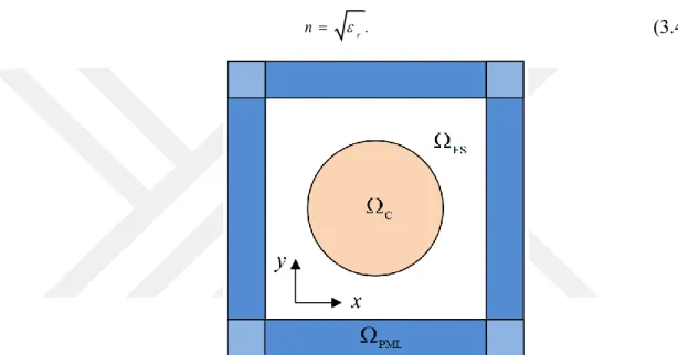
Figure 3. 3: Definition of the computational domain composed of a dielectric cylinder (Qc ) embedded in the free space (Q FS ) and truncated by PML. ... 22
Figure 3.4: A possible discretization of the computational domain at R
=
1.5A, and N xN=9x9 for each element (here, only elements corresponding to QFS and Qc are sho\VJl) ... 23Figure 3.5: Visualization ofphotonic nanojet atR
=
3.5A andn=
1.6 ... 24Figure 3.6: 3D visualization ofphotonic nanojet atR = 3.5A andn
=
1.6 ... 24Figure 3. 7: Visualization ofphotonic nanojet at R = 5A andn
=
1.6 ... 25Figure 3.8: Visualization ofphotonic nanojet atR
=
6.5A andn=
1.4 ... 25Figure 3. 9: Color mapping of field intensity as obtained by FDTD method for various shapes of dielectric micro-cylinders ... 27
Figure 3. 10: Visualization of the evolution ofa photonic nanojet for R
=
3.50A and n=
1.7 . WGM representation gives m=28 and I=
2 ... 28Figure 3. 11: Visualization of the evolution of a photonic nanojet for R = 4.50A .... 29
Figure 3. 12: FDTD visualization of the evolution of a photonic nanojet for. ... 29
Figure 3. 13: Magnitude of magnetic scattered-incident field inside the cylinder for R = 4A and n = 1.4 .as obtained by Mie theory ... 31
Figure 3. 14: The magnitude ofthe total magnetic field inside the cylinder ... 32
Figure 3. 15: The magnitude of the total magnetic field inside the cylinder at ... 32 Figure 4. 1: Total field absolute value inside and outside of the dielectric cylinder of
radius R
=
3.5A due to an illuminating plane wave as computed by SEM inthe neighborhood of resonance at (a) n=I.6995, (b) n=I.7000
(maximum), (c) n=1.7005, and (d) n=1.7010 ... 37
Figure 4. 2: (a) Total field absolute value inside and outside of the dielectric cylinder of radius R
=
3.5/L due to an illuminating plane wave as computed bySEM in the neighborhood of resonance at (a) n=1.6, (b) n= 1.8 ... 38
Figure 4.3: Total field magnitude inside and outside of the dielectric cylinder of refractive index n
=
1.7 due to an illuminating plane wave as computed by SEM in the neighbourhood of resonance at (a) R = 3.5005, (b)R=3.5010, respectively ... 38
Figure 4. 4: Magnitude of the electric field profile along the x-axis pa~sing through the micro-cylinder's center. Data presented in figure 4.1 is used to plot the transverse field variations for four cases: (a): n = 1.6995, (b)
n = 1. 7000 (on-resonance), (c) n = 1.7005, and (d) n = 1.7010 ... 38
Figure 4. 5: Magnitude of the total field inside and outside of the dielectric cylinder of radius R
=
4.5/L due to an illuminating plane wave as computed bySEM in the neighbourhood of resonance at (a) n = 1.9995 , (b)
n =2.0000 (maximum), (c) n=2.0005, and (d) n=2.0010 ... 39
Figure 4.6: Field magnitude inside the dielectric cylinder of radius R
=
3.5/L due toan illuminating plane wave as calculated by Mie theory in the
neighbourhood of resonance at (aI) n = 1.6795, (bI) n = 1.6800, (c1)
n
= 1.6805 (maximum). The contributions of the modem=
27 to the overall intensity are shown in (a2), (b2) and (c2) atn
=
1.6795, 1.6800, and 1.6805 , respectively ... 40 Figure 4. 7: Total field magnitude inside the dielectric cylinder of radius R=
4.5..1,and at n = 1.97259 due to an illuminating plane wave as calculated by Mie theory: (a) For m := 0 -+ 120 , (b) The contribution of the mode number m = 3 6 ... 41 Figure 4. 8: Illumination by Bessel's beam at
r
=
0.6 (a) magnitude of the excitingincident field produced by Bessel's beam, and (b) magnitude of the total scattered-incident field (3D view) inside and outside the dielectric
cylinder whose parameters are R, n
=
3 .5A, 1. 7 ... .46 Figure 4. 9: Magnitude of the total field inside and outside a dielectric cylinder ofradiusR
=
2.8..1, for (a) 111=
1.5, and (b) 111=
1.5,112=
1.33 ... 46 Figure 4. 10: Magnitude of the total field inside and outside a dielectric cylinder ofradiusR
=
3.5..1, at 111=
1.7, and has a square region of 112=
1.33 and2.4AX2.4A atitscenter. ... 47
Figure 4. 11: Magnitude of the total field along x-axis for the case in figure 4.8 ... 47 Figure 4. 12: Magnitude of the total scattered-incident field due to plane wave
illumination inside and outside the dielectric cylinders of radius and refractive index (a) (R,n)
=
(3.5198A, 1.69) , (b) (R,n):= (3.2245J.,1.85) , (c)(R,n) = (2.84749U,2.1) and (d) (R,n)
=
(2.7198007 A, 2.2) ... 49 Figure 4. 13: Magnitude of the total field along the x-axis for the case in figure 4.8 50 Figure 4. 14: Radius versus refractive index variation for the same type of resonancemode with dielectric micro-cylinder. Data points captured with SEM are
plotted with markers. Cubic spline extrapolation of the relation between the physical parameters defining the micro-cylinder where two-ring resonance takes place ... 50 Figure 4. 15: Magnitude ofthe total field resulting from a plane-wave illuminated
dielectric cylinder of (a) R = 5.OA ,n = 1.4, and (b) R = 4.5A, n = 1.905 .
... 52 Figure 4. 16: Schematic representation of the photonic structure illuminated by a
point source ... 53 Figure 4. 17: Real part of the electric field generated by a point source ... 53 Figure 4. 18: Illumination by a point source placed at different positions for
R,n = 3A, 1.5 (a) d
=
ISA, (b) d=
lOA, (c) d = SA, (d) d = 3A . ... 54 Figure 4. 19: Illumination by a point source placed at different positions forR = 3.06267A, n
=
1.95 (a) d=
lOA, (b) d = SA, the associated field magnitudes along x-axis are shown in (c) and (d), respectively ... 55 Figure 5.1: The schematic of the hemicylindrical particle and definition of forwardand backward excitation ... '" .... 60 Figure 5. 2: The magnitude ofthe total scattered field due to plane wave illumination (backward excitation) inside and outside the hemicylinder with the radius and the refractive index values (a) (R,n)=(3.5A,1.7), (b)
(R,n)=(2.93,.1,,2.0) ... 61 Figure 5.3: The magnitude of the total scattered-incident field due to plane wave
illumination (back excitation) along the line of symmetry for R=2.93,.1,
and different refractive indices ... 62 Figure 5. 4: The magnitude ofthe total scattered field for forward plane wave
illumination of the hemicylinder with the radius and refractive index of (a) (R,n)=(1.5,.1,,1.65), (b) (R,n)=(1.5,.1,,1.55), (c) (R,n)=(2.93,.1,,2.0), and (d) (R,n)=(2.96,.1,,2.0) ... 62 Figure 5.5: The magnitude of the total scattered field in the case of forward
excitation along the line of symmetry while setting n=2.0 and
R={2.93,.1,,2.96,.1,} ... 63
Figure 5. 6: The magnitude of the total scattered field for forward plane wave illumination of the hemicylinder with the radius and refractive index of (R,n)=(2.96,.1,,1.46) ... 64 Figure 5. 7: The GLL grids ( N x N = 9 x 9) in the 12 el ements for a regular cylinder
(a) ofradiusRo =4,.1" and (b) for a corrugated cylinder of
Ro
=
4,.1" ~ = 6, n~=
4, and j3=
0.3 ... 65 Figure 5. 8: The dielectric corrugated cylinder of average radiusRo
= 4.SA plotted at(a) ml=10,m2=2, and,B=0.2,(b) m1=10,m2=2, and,B=O.4,(c)
m1 = 10, m2
=
4, and,B = 0.2, and (d) m) = 10, m2=
4, and,B = 0.4. Perfectcylinders with
Ro
= 4.SA are superimposed in each case for easyinspection of the irregular boundaries with respect to ideal case ... 67 Figure 5. 9: Field magnitude inside and outside the dielectric cOlTUgated cylinder of
refractive index n= 1.5 and average radius ~ = 4.SA due to a normally
incident plane-wave as computed by SEM for the four cases shown in Figure 5.8 ... 68 Figure 5. 10: Field magnitude inside and outside the dielectric corrugated cylinder of
refractive index n = 1.7 and average radius Ro = 2.SA due to a normally incident plane-wave as computed by SEM for (a) a circular cylinder, (b)
mj =10,m2 =2, and,8=0.111, (c) mj =10,m2 =2, and ,8=0.222, (d) mj = 10, n12 = 4, and ,8=0.111, and (e) mj = 10, m2 = 4, and
P
= 0.222 ... 69Figure 5. 11: The dielectric corrugated cylinder of average radius Ro = 2.5/1, (a) plotted atm1 = 16, m2 = 4, and
f3
= 0.18, and (b) the SEM solutionCI
EzI)
at n = 1.452 due to a normally incident plane-wave propagating in
positive x direction ... 71 Figure 5. 12: Field magnitude inside and outside the dielectric corrugated cylinder of
average radius Ro
=
2.5/1" m1=
16, m2=
4 due to a normally incident plane-wave as computed by SEM for (a) n = 1.452,P
=
0.12, (b)n = 1.452, P
=
0.18, (c) n = 1.452, P=
0.22, and (d) n=
1.455, P = 0.18 . ... 71 Figure 5.13: SEM solution to the incident-scattered field (E:nc +E:) inside andoutside of a magneto dielectric cylinder of radius R
=
3/1, and wither =l1r =1.5 ... 73 Figure 5. 14: SEM solution to the real of incident-scattered field (E~nc
+
E:) insideand outside of a magneto dielectric cylinder of radius R = 3/1, and with
I1r =3ander = (4-l1r)/(2I1r +1) ... 74 Figure 5. 15: 1 E;nc + E: I inside and outside of a magneto-dielectric cylinder of radius
R =3/1, and with flr
=
3 and&r=
(4-flr)/ (2flr+
1) ... 74 Figure 5. 16: Magnitudes of total fields(I
E~nc+
E:I)
for a micro-cylinder of radiusR=3/1" (a) Gr =2,,ur=1 ,(b) &r=2,,ur=0.5,(c) Gr =0.5,,ur=2(c)
field magnitudes along propagation direction, i.e., along y
=
0 , for the cases in part (a) and (b). Dimensions are nom1alized with /1, ... 75 Figure 5. 17: 1 E:nc+
E: 1 inside and outside of a magnetodielectric square cylinderwith 3/1, x 3/1, and whose I1r
=
1.4 and Gr = 111.4 ... 76LIST OF TABLES
Table 2. 1: Maximum relative errors of FDM and SEM for the problem defined in
Eq. 2.30 ... 15
Table 2. 2: Maximum errors of SEM and FEM for the problem defined in Eq. 2.32 . ... 17
Table 2. 3: Maximum relative errors of FEM and SEM for the problem defined in Eq. 2.33 ... 18
Table 4. 1: CR, n) pairs at which 2-ring resonance appears ... 49
Table 5.1: Variations of radius in terms of incident wavelength ... 66
Table 5. 2: Variations of radius in terms of incident wavelength ... 67
ABBREVIATIONS
ID : One Dimension
2D : Two Dimension
ABC : Absorbing Boundary Condition
BC : Boundary Condition
CPU : Central Processing Unit
FEM : Finite Element Method
FDM : Finite Difference Method FDTD : Finite Difference Time Domain FWHM : Full Width at Half Maximum
GLL : Gauss-Legendre-Lobatto
PDE : Partial Differential Equation PML : Perfectly Matched Layer
PNJ : Photonic Nano Jet
SEM : Spectral Element Method
TE : Transverse Electric
TM : Transverse Magnetic
WGM : Whispering Gallery Mode
LIST OF SYMBOLS
k : One Dimension
A, : Wavelength
e
: Angle of incidenceE : Electric field
Einc : Incident electric field ESC : Scattered electric field
n
e : Deformed elementn
st : Standard element a : Attenuation factor JI : Magnetic permeability f.1r : Relative permeability 5 : Permittivity 5r : Relative permittivity R : Radius n : Refractive indexa
: Partial derivative xvii1 1. INTRODUCTION
“Read in the name of your Lord. Who created. Created man from a clot of congealed blood. Read, and your Lord is Most Generous. Who taught knowledge by the pen, taught man what he did not know”
__Al Alaq, The QURAN
Human beings should acknowledge and not forget the Scottish physicist and mathematician James Clerk Maxwell (1831-1879), who combined these laws into a set of partial differential equations, known as Maxwell’s equations. Maxwell didn’t only simplify and reformulate these laws, but also he added another term to the differential equation corresponding to Ampere’s circuital law. This addition was the historical step that brought humanity to the technology that we enjoy nowadays. It was the prediction of existence of electromagnetic waves.
Well, progress and improvements in science occur successively, exactly as climbing a building by a ladder. Maxwell’s work wouldn’t appear at all if for instance, but not limited to, Charles Austin de Coulomb (1736-1806), Luigi Galvani (1737-1790), Hans Christian Oersted (1777-1851), Andre Marie Ampere (1775-1836), and Michael Faraday (1791-1867) didn’t form the previous steps in that ladder. In fact, the same level of acknowledgment should be given to these scientists and all others who lived before and after. As a student, and here I confirm that I don’t interpret being a student the one who seeks a certificate but rather who seeks the knowledge, I acknowledge all people who contributed to science starting from the first man who thought about optics and ending with my advisor.
1.1 Brief History About Transparent Spheres
Over the last 400 years, scientists have been attracted by transparent spherical particles. In fact, since ancient times, it has been known that a garden shouldn’t be watered during the afternoon because water droplets may cause sunburn to the leaves. Pliny Elder (AD 23-79) reported on the incendiary action of spheres made of glass and
5
Another classification of electromagnetic problems is based on the domain in which the solution is sought; that is, frequency domain and time domain. For each domain, modelling differential equations or integral equations can be utilized. Throughout this thesis, differential equations in frequency domain are used.
Spectral element method (SEM) has been recently applied to electromagnetic problems [53-58] and attracted the attention of computational electromagnetic community. The attraction of this method is mainly due to the accuracy achieved for much less degrees of freedom.
1.4 Contribution Of The Thesis
This thesis is based on the following publications that cover most of the contributions: 1. I. Mahariq, H. Kurt, H. I. Tarman, and M. Kuzuoğlu, “Photonic Nanojet Analysis by Spectral Element Method”, IEEE Photonics Journal, 6(5), pp. 1-14, 2014.
2. I. Mahariq, and H. Kurt, “On- and off-optical-resonance dynamics of dielectric microcylinders under plane wave illumination”, Journal of the Optical Society of America B, Vol. 32.6, pp. 1022-1030, 2015.
3. I. Mahariq, V. Astratov, and H. Kurt, “Persistence of photonic nanojet formation under the deformation of circular boundary”, Journal of the Optical Society of America B, 33.4: 535-542, 2016.
4. I. Mahariq, and H. Kurt, “Strong field enhancement of resonance modes in dielectric micro-cylinders”, Journal of the Optical Society of America B, 33.4: 656-662, 2016.
5. I. Mahariq, H. Kurt, and M. Kuzuoğlu, “Questioning Degree of Accuracy Offered by the Spectral Element Method in Computational Electromagnetics”, Applied Computational Electromagnetics Society Journal, vol. 22.7, 2015. 6. I. Mahariq, N. Eti, and H. Kurt, “Engineering Photonic Nano-jet Generation”,
Computational Electromagnetics International Workshop, July 4-6, 2015. Izmir, Turkey.
7. N. Eti, I. Mahariq, and H. Kurt, “Mode Analysis and Light Confinement of Optical Rib Waveguides in Various Air Slot Configurations”, 17th International Conference on Transparent Optical Networks, July 5-9, 2015, Budapest, Hungary.
6
The following manuscripts are currently under review:
1. I. Mahariq and H. Kurt, “Investigation of Strong Field Enhancement Resulting from Magnetodielectric Cylinders”, IEEE Photonics Technology Letters. 2. I. Mahariq, I. H. Giden, I. V. Minin, O. V. Minin, and H. Kurt “Strong
electromagnetic field localization near the surface of hemicylindrical particles”, Optical and Quantum Electronics.
1.5 Outline Of The Thesis
In chapter 1, an introduction is presented including some history about transparent spheres. Also, a brief summary of the numerical methods applied for solving Maxwell’s equations.
Then, the formulation of the spectral element method required to solve Maxwell’s equations governing the photonic structures is presented in chapter 2. In addition, the deterioration of spectral element method resulting from the elemental deformation is discussed. The chapter ends by a quick comparison between spectral element method, finite element method and finite difference method in terms of accuracy in both one and two dimensional problems.
Chapter 3 discusses the properties and analysis of photonic nanojets and whispering gallery modes resulting from a plane-wave excited micro-cylinders. In chapter 4, a detailed discussion about the dependency whispering gallery modes on the physical parameters of cylinders is included. The corresponding spectral element solutions is then compared with Mie theory solutions. Numerical tracking to the physical parameters combinations is also presented. The chapter also investigates the behaviour of photonic jets and whispering gallery modes under different excitation schemes. Chapter 5 presents the analysis about the deformation of cylinders and how it affects the photonic nanojet characteristics and whispering gallery modes. The same chapter discusses the field analysis when magnetic cylinders are considered. Chapter 6 finished the thesis presentation by some conclusions.
9
governs the field attenuated in y-direction in PML region,
2 2 2 2 2 1 u 1 u a k u 0 , a x a y (2.4)
governs the field attenuated in both x- and y- directions in PML region, and
2 1 . u 2 u 1 i n c, r r z r k k E (2.5)
is satisfied wherever there is a dielectric object, where; k 2 / is the wave
number, with being the wavelength, a 1 / jk , is the attenuation factor (a real number that defines amount of attenuation), r is the relative permittivity of the
scatterer, r is the relative permeability of the scatterer, and
in c z
E is the incident wave.
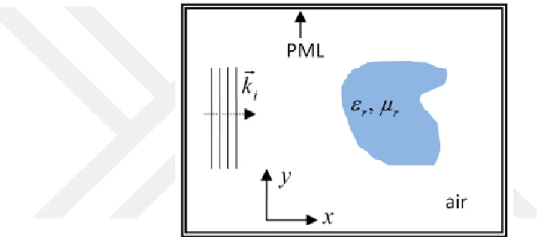
Figure 2. 1: A typical electromagnetic scattering problem composed of a dielectric (or magnetic) scatterer embedded in a free-space region, and domain truncation is performed by the perfectly matched layer.
Figure 2.1 shows a typical electromagnetic scattering domain which is composed of a scatterer of an arbitrary shape. The scatterer is embedded in a free-space region, and the domain truncation is performed by the perfectly matched layer. At this point, a tensor is introduced so that all of the previous equations can be represented in one
equation. The tensor is defined as:
1 1 2 2 0 , 0 (2.6) where; 1 1 2 2 1 a a
for x-decay in the PML region,
1 1 2 2 1 a a
10 1 1 2 2 1 1 a a
for a corner (xy-decay) in the PML region with a 1
in free-space region, and rbeing greater than 1 in the scatterer only, and 1 elsewhere.
Thus, the set of all partial differential equations governing an electromagnetic scattering problem can be written as follows:
2 2 . u+ a u 1 in c. rk k r Ez (2.7)It is worth to mention that for transparent dielectric material and for free-space is
1 r
. In addition, r 1 in the dielectric material only, and r 1 elsewhere. In fact,
when r 1, the right-hand side of equation (2.7) vanishes to zero. In the next section,
we provide the spectral element formulation for the Helmholtz equation as expressed in equation (2.7) which must be satisfied in a typical electromagnetic scattering and/or radiation problem.
2.3 SEM Formulation
As discussed in the previous section, a typical electromagnetic scattering and/or radiation problem in the frequency-domain can be defined as:
2 2 . u+ a u 1 in c rk k r Ez (2.8a) for 2 ( x , y ) x subject to the boundary conditions:
D n N
u f , u g ,
(2.8b)
on the boundary D N .
SEM formulation involves two function spaces, namely, test and trial spaces. An approximate solution to equation (2.8) is sought in the trial space
D n N
U u H | u f , u g .
(2.9)
The residual resulting from the substitution of the approximate solution from the trial space into equation (3.8) vanishes in the process of projection onto the test space
V { v H v 0} .
D
(2.10)
The projection is performed by using the weighted inner product operation: v , u v u d
11
in the Hilbert space H where overbar denotes complex conjugation. The projection procedure 2 2 a (v, . u u 1 in c) 0 rk k r Ez (2.12)
leads to the variational (weak) form
2 2 ( v) u d x a v u d x v g d x 1 v d x N in c r z k k E
(2.13)after integration by parts that introduces the boundary integrals. The trial function is then decomposed as follows
h b u u u , where D h u 0 and D b u f , (2.14) resulting in h h b ( v) u d a 2 v u d x ( ) u d x k v
x
2 b a v u d x v d x 1 v d x N 2 in c r z k g k E (2.15)after substitution into equation (2.13). The boundary conditions are now in place in the variational form with the introduction of the particular solution ub satisfying the nonhomogeneous Dirichlet boundary condition.
Adapting the formulation to an arbitrary domain geometry is achieved in two steps. The first step involves partitioning of the domain into mutually disjoint elements:
M
1 e M e
e = 1
... ... .
(2.16)
A typical integral in the variational form then becomes
e M h h e 1 v u d v u d ,
x
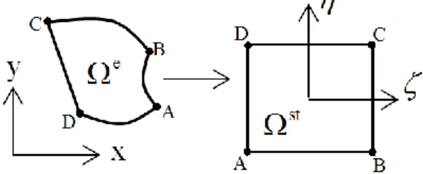
x (2.17)due to the linearity of integration operation. The second step is the introduction of the standard square element
st 2
( , ) | 1 1, 1 1
(2.18)
that will standardize and facilitate the integral operations over a general quadrilateral element e with curved sides through mapping:
e e
1 2
12
In another word, in order to perform the operations of integration and differentiation in an element e that may have an arbitrary shape and orientation as shown in Figure 2.2, the introduction of the one-to-one elemental mapping defined in equation (2.19) is necessary. In fact, this mapping is also onto, which in turn becomes isomorphic transformation. The isomorphism here tells us that inverse transformation exists.
Figure 2. 2: Mapping an element e to the standard elements t. The differential operations can then be converted using the rules:
e e 1 1 e e 2 2 d x d d y d J , e e 2 1 e e 2 1 x 1 y -, - J (2.20)
where J is the determinant of the Jacobian J.
Numerical implementation of the procedure requires introduction of a spatial discretization that will facilitate the numerical evaluation of the derivatives and the integrals. This is equivalent to taking the trial and test spaces as finite dimensional spaces for which space of polynomials is the convenient choice. Jacobi polynomials as eigenfunctions of singular Sturm-Liouville differential operator provide a good basis for this space [70]. Numerically stable interpolation and highly accurate quadrature integration approximation techniques are provided by nodes and weights associated with Jacobi polynomials. In particular, Legendre polynomials are the convenient choice in that they are orthogonal under the weighted inner product with unity weight 1. The associated roots m as nodes provide the stable form of interpolation N m m m 0 u ( ) u ( ) L ( )
(2.21)where L denotes respective Lagrange interpolants with the typical form
k N ( ) k ( ) 0 k L ( ) (2.22)
13
satisfying the cardinality propertyL ( )k k . This in turn provides the means for
evaluating the derivatives, say,
k k m N N d m m k m m k d m 0 m 0 D u ( ) u ( ) L ( ) u ( ) L ( ) (2.23)
where Dk m is referred to as the differentiation matrix. It also provides
Gauss-Legendre-Lobatto (GLL) quadrature 1 N k k k 0 1 u ( ) d u ( )
(2.24)which is exact for the integrand of a polynomial of degree2 N 1 . These can easily
be extended to two dimensions over the tensor grid ( , k ) with the mapping
functions i( , ) constructed using the linear blending function approach [71-72].
As mentioned above, the nodal basis for the reference element is usually built by Lagrangian basis polynomials associated with a tensor product grid of GLL nodes. Figure 2.3 shows such a grid for a ninth-order polynomial space. In one direction, the GLL grid nodes [ 1,1], 0 N are the roots of the polynomial:
2 d N( ) (1 - ) d P x x x (2.25)
where P (x )N is the Legendre polynomial of degree N in [ 1,1] : 0 1 n 1 n n 1 ( ) 1, ( ) , 2 n 1 n ( ) ( ) ( ), n 1 . n 1 n 1 P x P x x P x x P x P x (2.26)
14
Figure 2. 3: GLL grid nodes on the reference element for a ninth-order polynomial space (nodes are represented by the intersections of horizontal and vertical lines).
Figure 2. 4: Plot of first six Legendre polynomials.
It is important here to demonstrate the accuracy of the spectral element in one element of square shape and deformed shape. In the following section, the effect of element deformation on the accuracy of spectral element method is investigated.
2.4 The Accuracy Of SEM, FDM And FEM
To get an insight about the accuracy gained from SEM, when compared to other numerical methods, demonstrations are performed using numerical examples. For this purpose, a comparison is first carried out between SEM and FDM with a stencil
15
composed of 3 nodes in one dimension. We considered the following one-dimensional boundary-value problem: 2 2 2 1 .1 0 , in th e in te rv a l [0 ,1 .1] w ith (0 ) 1, (1 .1) e j k d u k u d x u u (2.30)
where k 2 . We define an error measure as follows:
, , , m a x i i e x ac t i n u m e ri c al i e x ac t u u E rr u (2.31)
where; ui e x a c t, is the exact solution (for this problem, it is e j k x
), and
, i n u m e r i c a l
u is the
numerical solution obtained by the specified numerical method at the ith node in the
computational domain.
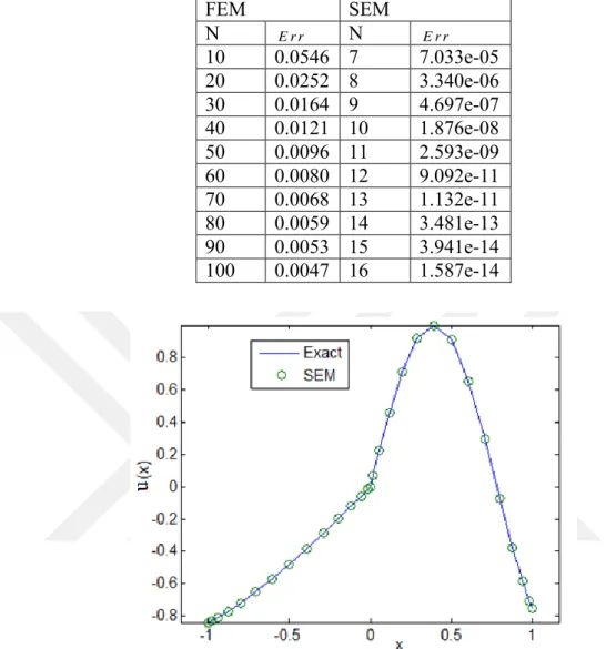
In Table 2.1, the maximum relative errors for both FDM and SEM are presented as the number of nodes (N) increases in both methods. Obviously, it can be observed that the errors of FDM are slowly decaying although the number of nodes is chosen in the order of 10. On the other hand, SEM shows high accuracy with much fewer number of nodes. That is, the accuracy obtained by FDM at 100 nodes can be achieved by 8 nodes with SEM.
Table 2. 1: Maximum relative errors of FDM and SEM for the problem defined in Eq. 2.30. FDM SEM N E r r N E r r 10 0.1840 7 0.0103 20 0.0524 8 0.0012 30 0.0238 9 1.455e-04 40 0.0135 10 1.608e-05 50 0.0087 11 2.074e-06 60 0.0060 12 2.308e-07 70 0.0044 13 2.570e-08 80 0.0034 14 2.624e-09 90 0.0027 15 2.613e-10 100 0.0022 16 2.420e-11 110 0.0020 17 2.318e-12
16 2 2 2 2 2 0 , in [ 1, 0 ], a n d 4 0 , in [0 ,1]
w ith ( 1) sin ( 1), (1) sin ( 4 ). d u u d x d u u d x u u (2.32)
In fact the solution of (2.32) is u x( )sin (c ),x with c 1 in [ 1, 0 ], and c 4 in [0 ,1].
However, for error calculations, to avoid division by zero, we compute the error (only for this problem) as the maximum difference between the exact solution and the numerical solution. The comparison is shown in Table 2.2 in which N represents the number nodes in each sub-domain. Again, it can be seen that SEM accuracy is much higher than that of FEM. Figure 2.5 shows the plot of the solution obtained by SEM for 15 nodes in each subdomain.
It is worth also to compare FEM and SEM in a two dimensional boundary value problem. For this purpose, the point source problem (2D Green’s function) is considered. This problem is governed by the Helmholtz equation:
2 2 ( ),
u k u r
(2.33)
wherek 2 / , and is the wavelength. To avoid the singularity at the origin, the homogenous Helmholtz equation is solved inside a square element (Ω) of dimensions
and 1, and Ω is defined in the xy-plane so that the point (0,0) does not belong to this element. On the boundary ∂Ω, the exact solution to (2.33), which is expressed in terms of Hankel function of the second kind zero order as follows: (
( 2 ) 0
( ) ( / 4) ( | r |)
u r j H k , is applied as boundary conditions, where | r | is the euclidean distance from the origin to a point | r | on the boundary ∂Ω. Right-triangle elements are utilized in meshing the problem. Figure 2.6 shows the solution obtained by FEM at a grid of 2 02 0nodes. As observed from Table 2.3, the error profile in 2D does not differ from that of 1D case.
17
Table 2. 2: Maximum errors of SEM and FEM for the problem defined in Eq. 2.32. FEM SEM N E r r N E r r 10 0.0546 7 7.033e-05 20 0.0252 8 3.340e-06 30 0.0164 9 4.697e-07 40 0.0121 10 1.876e-08 50 0.0096 11 2.593e-09 60 0.0080 12 9.092e-11 70 0.0068 13 1.132e-11 80 0.0059 14 3.481e-13 90 0.0053 15 3.941e-14 100 0.0047 16 1.587e-14
Figure 2. 5: Exact and SEM solutions of the problem defined in Eq. 2.32.
Figure 2. 6: FEM solution of the 2D point source problem defined in Eq. 2.33.
18
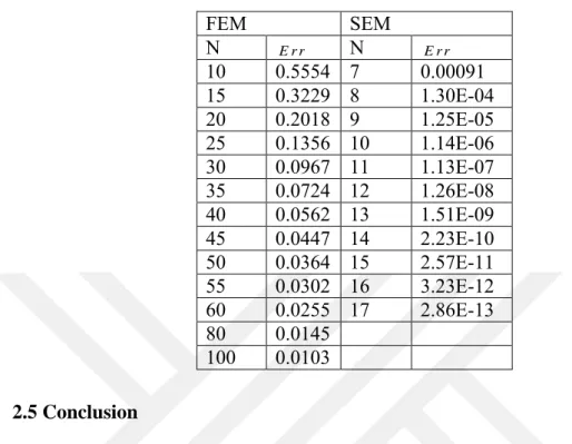
Table 2. 3: Maximum relative errors of FEM and SEM for the problem defined in Eq. 2.33. FEM SEM N E r r N E r r 10 0.5554 7 0.00091 15 0.3229 8 1.30E-04 20 0.2018 9 1.25E-05 25 0.1356 10 1.14E-06 30 0.0967 11 1.13E-07 35 0.0724 12 1.26E-08 40 0.0562 13 1.51E-09 45 0.0447 14 2.23E-10 50 0.0364 15 2.57E-11 55 0.0302 16 3.23E-12 60 0.0255 17 2.86E-13 80 0.0145 100 0.0103 2.5 Conclusion
In this chapter, the formulation of electromagnetic scattering and radiation problems based on the spectral element method is provided. This formulation considers also domain truncation by the perfectly matched layer. For this purpose, all the partial differential equations that govern over the perfectly matched layer, free-space regions, magnetic and/or dielectric objects, are put in a single representative form that defines a typical electromagnetic scattering in frequency domain. Numerical implementation by spectral element method is then applied.
Next, the effect of element deformation on the accuracy of spectral element method is investigated. As observed from the results, in quadrilateral elements having straight or curved sides the error was less than that of rectangular elements. Thus, in general, the accuracy can deteriorate if the aspect ratio of some elements is chosen to be large. One can notice from the presented errors that there is no safe range of the aspect ratio in which high accuracy is guaranteed.
Finally, a comparison is made in terms of accuracy among SEM, FDM and FEM. As it can be clearly seen from the results, SEM dominates the other numerical methods with extremely much less resolution at the same level of accuracy.
19 3. PHOTONIC NANOJET
In this chapter, we numerically investigate scattering of light by a dielectric, non-magnetic cylinder by SEM. By the aid of spectral element method and the perfectly matched layer formulations presented in this work, we accurately solve scattering by dielectric microcylinders. Interesting cases, which finite difference time-domain method couldn’t capture with a moderate resolution, are presented and discussed in this thesis. Verification of the obtained results is then presented using the analytical solution of Mie theory.
3.1 Numerical Analysis Of Photonic Nanojets
Light as an electromagnetic field interacts with different metallic or dielectric objects of any size and shape and provides novel features via scattering, reflection, refraction, and diffraction mechanisms [49-50]. To be more specific about light interaction with an object we can assume lossless (absorption free) dielectric micro-cylinders and excitation with a normally incident plane wave. The result of the interaction produces scattered light and strongly focused beam intensity at the back side of the medium (shadow side).
Optical engineering of micron sized dielectric cylinders and spheres produce nano-scale light manipulation. Divergence behaviour of the beam whether low or high, location of the focus (inside, at the boundary or outside of the cylinder), field enhancement, and transverse dimension of the spot size compared to the illuminating wavelength (how small with respect to the wavelength) are important parameters for the photonic jet. A substantial literature has been devoted to the verification of light focusing of photonic jet into sub-diffraction-limited sizes. Squeezing light at the shadow side as well as altering the location of focal point by means of different material and structural parameters (refractive index, radius, deformation, wavelength etc.) are unique properties to create interaction between enhanced intensity and matter interaction.
20
Experimental observation of photonic nanojets generated by latex microspheres of varying diameters was reported in Ref. 45 (See Figure 3.1). Low loss optical guiding of light can be accomplished by touching microspheres [48]. Propagation losses as low as 0.08 dB per microsphere was measured in the same study.
Photonic nanojets have been mainly explored by numerical methods based on FDTD analysis [30], [49], [58]. For instance, Figure 3.2 shows a visualization of a photonic nanojet as obtained by FDTD for a plane-wave-illuminated circular dielectric cylinder of 5 m diameter at a wavelength of 5 nm. The cylinder is embedded in vacuum and has a refractive index of 1.7. Very fine meshes are required in order to get accurate and reliable results with FDTD method. Besides, the excitation mechanism such as plane wave in free space may restrict the observation of special resonance modes. Later, analytical and semi-analytical attempts were introduced in the literature [50]. The majority of analytical studies are based on Mie theory. Rigorous Mie theory was used to analyse the fundamental properties of the photonic nanojet in [50]. Recasting eigenfunction solution of the Helmholtz equation into a Debye series. Ref. 30 provided detailed optics of photonic nanojets on dielectric cylinders.
Figure 3. 1: Experimental observation of a photonic nanojet viewed along the optical axis of a 5 m -diameter dielectric sphere made of glass, [48].
21
Figure 3. 2: Visualization of a photonic nanojet of a plane-wave-illuminated circular dielectric cylinder of 5 m diameter and has a refractive index of 1.7. [30].
As mentioned previously to have accurate results with FDTD method it is necessary to use finely discretized mesh which is a huge burden on the computational resources. Therefore, it is important to check/verify results with an alternative numerical method. In the present work, we implement the spectral element method to solve for the scattered electric field inside and outside the dielectric cylinder.
3.2 Photonic Nanojet Resulting From Dielectric Micro-cylinders
In the case of photonic nanojet where the scatterer is assumed to be an infinitely-long dielectric cylinder, the problem can be considered as a two-dimensional one when an incident plane wave propagating in a direction perpendicular to the cylinder axis is assumed. We consider an incident plane wave propagating in x-direction and the electric field is polarized in z-direction (i.e., in a transverse magnetic mode (TMz)):
e x p ( ) i n c
z z
E a j k x (3.1)
To solve the problem numerically, we should truncate the unbounded domain. Again, the formulation of the perfectly matched layer presented in chapter 2 is utilized for the domain truncation. Figure 3.3 shows, in the xy-plane, a dielectric cylinder represented by C , free space region represented by F S , and the PML region denoted by P M L
, which represents the region surrounding F S . On the outer boundary of P M L ,
zero-dirichlet boundary condition is simply imposed. In F S , the homogenous Helmholtz
equation is satisfied: 2 2 0 , s s z z E k E (3.2)
22
in which s z
E stands for the scattered electric field and polarized in the z-direction (TMz
polarization is considered), andk is the wave number. While in C , the following
Helmholtz equation can be derived:
2 2 1 , s 2 s in c z r z r z E k E k E (3.3)
where; r is the relative permittivity, and i n c z
E represents the incident plane wave.
Throughout this work, we assume that the medium in non-magnetic (r 1). In P M L
, the set of partial differential equations derived in chapter 2 must be satisfied. Under these assumptions, the refractive index is related to the relative permittivity as follows:
.
r
n (3.4)
Figure 3. 3: Definition of the computational domain composed of a
dielectric cylinder (C) embedded in the free space (F S ) and truncated by
PML.
Before we proceed further, it is worth to mention that the scattering dielectric cylinder is embedded in the free space that has a unity refractive index. From practical viewpoint, the cylinder can be embedded in another dielectric material that has a refractive index different than one, but it should be less than that of the scattering cylinder in order to obtain a photonic nanojet. What is important here is that the effective refractive index (ne f f ) which is expressed by:
, C e f f m n n n (3.5)
where; nC and nm are the refractive indices of the cylinder and the surrounding
material, respectively. In this work, we assume that the surrounding material is free space and we denote the effective index by n which, in turn, is the refractive index of
23
the scattering cylinder. The radius of the cylinder, denoted byR , is normalized with
the wavelength .
A possible discretization of the computational domain by spectral element method when the dielectric cylinder radius isR 3.5 , is shown in Figure 3.4. In this figure, the GLL nodes are chosen as NN=99 in each element for demonstration purpose.
However in this work, finer resolutions are considered depending onR , for instance,
whenR 3.5 , the grid size of 3030 in each element is considered when the domain
elements are chosen as shown in Figure 3.4 in order to achieve approximately 14 points per wavelength). It is important to mention that the number of elements should be increased as the radius of the cylinder increases due to the grid distribution of GLL nodes and since the radius is normalized with the wavelength.
Figure 3. 4: A possible discretization of the computational domain at 1.5
R , and N N=9 9 for each element (here, only elements
corresponding to F S and C are shown).
Typical field solutions of photonic nanojets obtained by spectral element method are shown in Figure 3.5 for the cylinder radiusR 3.5 , and for a refractive indexn 1 .6
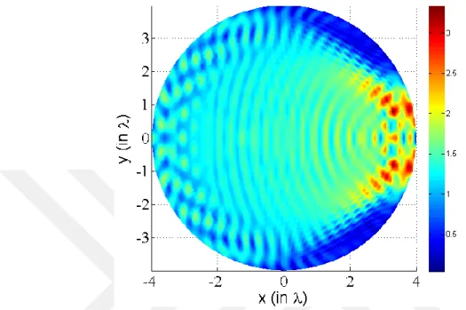
. The plots in this chapter are illustrated using color map. In Figure 3.6, the photonic nanojet in Figure 3.5 is shown 3D. Figures 3.7 and 3.8 illustrate different photonic nanojets at (R 5 , n1 .6) and at (R 6.5 , n 1 .4), respectively.
24
It is worth to mention that, after obtaining the solution by spectral element method, which represents the scattered field, the incident plane wave is added to the scattered field in the subdomains C and F S only. One can produce the same spatial light
distribution for the case where FDTD method is used. We have performed FDTD study and verified the exact photonic nanojet creations. With the application of SEM in frequency domain, it is easy to decompose the total field into incident and scattered field components.
Figure 3. 5: Visualization of photonic nanojet atR 3.5 andn 1 .6.
25
Figure 3. 7: Visualization of photonic nanojet at R 5 andn 1 .6 .
The results presented in the previous figures demonstrate the capability of spectral element in the analysis of photonic nanojet generation. The input source interacts with the cylindrical object and gets focused at different locations as we change the radius and refractive index of the dielectric material. The focal point appears close to the surface in Figure 3.5 and it moves away from the back side along the optical axis (y=0 line) in Figures 3.7 and 3.8.
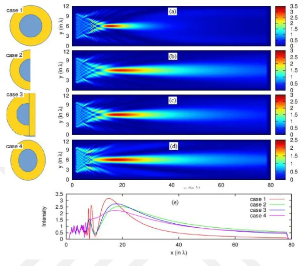
26 3.3 Long Photonic Nanojets
In addition, photonic nanojets results with different structures. For instance, a loss-free dielectric micro-cylinder composed of two different materials is considered also in this section. The inner material has a refractive index and radius of n3 1 .4 0 and R3,
respectively. Whereas the outer material is defined by n2 1 .5 0 and R2. The cylinder
is placed along z-axis and embedded in a medium whose refractive index is n11 .3 3.
This structure is illuminated by an incident plane wave propagating in x-direction and perpendicular to the cylinder axis. Four different cases are analysed by FDTD method and the results are presented in Figure 3.9. In case 1, the geometry is circular with
3 2 .2
R and R2 2 .5 , where stands for the wavelength. Whereas in case 2, half
of the cylinder is considered under same radii, and a rectangular slab is added for case 3. In case 4, we shrank the geometry to have an elliptic structure with R3x 2 .0 0 ,
3y 2 .3 2
R , R2x 2 .5 0 , R2y 2 .9 0 . In all cases, it can be clearly observed that the
generated photonic nano-jets are really ultra-long especially for case 4 (about 2 0 in x-direction). In addition, as seen from the intensity plot in Figure 3.9 (e), increasing the length of the nano-jet is accompanied with the decrease in the maximum field intensity.
27
Figure 3. 9: Color mapping of field intensity as obtained by FDTD method for various shapes of dielectric micro-cylinders.
3.4 Whispering Gallery Modes In Dielectric Cylinders
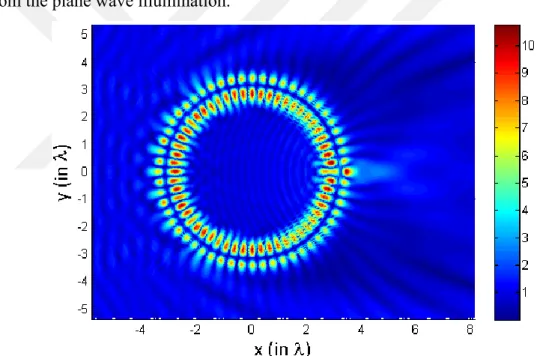
Plane wave illumination of dielectric micro cylinders with FDTD method always produces an expected lensing/focusing effect so that the planar wave front of light gets tilted and focused at the optical axis. In the next example, we try to emphasize the advantage of SEM analysis over FDTD method. For example, when we change the refractive index of the cylinder and keeping the radius constant at 3 .5 0 a resonance mode appears.
Figure 3.10 shows one of the captured resonance mode supported by a dielectric micro cylinder withR 3.50 andn 1 .7. The light focusing action with weak amplitude
can be seen at the interior part of the cylinder. On the other hand, strong field localization at around the small cylinder appears with a highly symmetric light distribution in the form of two rings. Light is trapped by total internal reflection. Similarly, when we change the radius of the cylinder to R 4.50 , the resonance
28
mode again occurs if the refractive index value becomes 2.0. The result is presented in Figure 3.11. Light distribution with five rings is highly symmetric and strong field localization takes place at the exterior part of the micro cylinder. The evanescent field that leaks out of the dielectric cylinder radially is apparent in the plot. Figures 3.10 and 3.11 can be attributed to whispering gallery mode (WGM). The representation WGMm,l indicates a WGM with the azimuthal mode number m and the radial mode number l. The resonance mode with different mode number is confined at the circumference of the cylinder by means of the total internal reflection mechanism. Using that notation we can express Figures 3.10 and 3.11 in terms of WGM resonances. By means of spectral element method we captured resonance modes as well as photonic nano jets cases. Commonly used FDTD method requires a different excitation scheme in order to gather the resonance modes of the micro-cylinder apart from the plane wave illumination.
Figure 3. 10: Visualization of the evolution of a photonic nanojet for 3.50
29
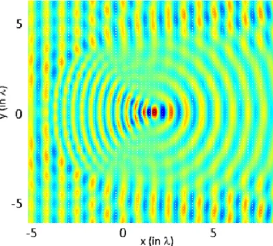
Figure 3. 11: Visualization of the evolution of a photonic nanojet for 4 .5 0
R and n 2 . WGM parameters are m=34 andI 4 .
We should point out that FDTD method gives us regular light focusing behavior but it does not indicate the creation of resonance mode. For instance, we have solved the problem at R 3.50 andn 1 .7 by FDTD method using MEEP (a FDTD-based
software developed by Massachusetts Institute of Technology-MIT). The corresponding real part of solution is shown on Figure 3.12. The plot is obtained by meshing the domain uniformly such that 40 nodes are used per one wavelength.
Figure 3. 12: FDTD visualization of the evolution of a photonic nanojet for 3.50
30
Phase matching condition has to be satisfied for FDTD method in order to excite the resonance mode. That condition requires special coupling techniques such as waveguide coupling or tapered optical fiber to excite the mode. The downside of the coupling approach is that the micro-resonator gets disturbed and the true resonance mode is modified due to the presence of the external waveguides.
3.5 Verification Of Whispering Gallery Modes
Photonic nanojet analysis can be performed analytically. Mie theory was intensively utilized in electromagnetic scattering problems. However, when the characteristic dimensions of the scattering object becomes much larger than the wavelength, improper algorithms may lead to considerable numerical errors [30]. In the examples presented in the previous section, where resonance takes places, the diameter of the micro-cylinder is larger than the wavelength but not too much. It is very important to check whether the analysis that Mie theory provides produces such resonance cases or not.
Itagi and Challener [30] provided the solution of the scattered light by a dielectric cylinder using Mie theory. Although their derivation is based on transverse magnetic mode (TE), we will use this analytical solution to verify our results. By Mie theory, the total-incident scattered magnetic field inside the cylinder can be expressed as:
0 ( , ) m c o s( ) m( ) m h a m J n k
(3.6)where; is the Euclidean distance from the z-axis to a point lying inside the cylinder,
is the azimuth angle, Jm denote Bessel function of the first kind of mth order, and k is the wavenumber. The coefficients am are defined as:
(1 ) ' (1 ) ' (1 ) ' (1 ) ' ( ) ( ) ( ) ( ) , ( ) (n ) ( ) (n ) m m m m m m m m m m H k R J k R H k R J k R a c n n H k R J k R H k R J k R (3.7)
in which R denotes the radius of the cylinder, H m(1 )is Hankel function of the first kind
of mth order, ' denotes the derivative with respect to the argument of the function, and the coefficients cm are given as:
1, 0 2 , 0 . m m m c j m (3.8)
31
This analytical solution is derived under the assumption that the cylinder is centered at the origin of the xy-plane. With the aid of this analytical solution, the magnitude of the magnetic scattered-incident field inside the cylinder is plotted for R 4 and
1 .4
n in Figure 3.13. Here, we note that the truncation of the series at m 1 5 0has
negligible effect on the solution.
Figure 3. 13: Magnitude of magnetic scattered-incident field inside the cylinder forR 4 and n 1 .4.as obtained by Mie theory.
Considering that the accuracy of spectral element method is very high, and one of the resonance cases is captured at a refractive index of n1 .7 , we have solved the problem at the neighborhood of n1 .7, for instance at n 1 .7 0 1 and at n 1 .6 9 9,
and the expected photonic nanojets were captured. So the index n 1 .7 is very critical. It should be noted that since the cylinder radius is larger than the wavelength, Mie theory provides an approximate solution instead of the exact solution.
In other words, the solution obtained by Mie theory shows that there is no resonance at 1.7. We have performed a search loop in the neighborhood of 1.7 and captured the same resonance cases obtained by spectral element method. Figures 3.14 and 3.15 show the magnitude of the total magnetic field inside the cylinder at (R 3.5 and
1 .6 9 0 5
32
Figure 3. 14: The magnitude of the total magnetic field inside the cylinder at 3 .5
R and n 1.6905.
Figure 3. 15: The magnitude of the total magnetic field inside the cylinder at 4.5
R and n 1 .8 9 1 1.
3.5 Conclusions
The formulation of perfectly matched layer is utilized together with SEM formulation. In addition, accuracy of SEM is demonstrated by solving for the scattered field from perfectly conducting cylinders. With the use of SEM, we could accurately perform
33
field analysis of photonic nanojets in dielectric lossless micro cylinders. Strong light focusing at the shadow side of the micro-cylinder is reported. Advantageous features of SEM allow the observation of commonly reported nanojet scenarios as well as the least pointed out transition region where resonance mode appears under certain conditions. The creation of whispering gallery mode types is plainly observed. One may be unaware of these special modes under the case of plane wave illumination with FDTD method that needs a coupling technique to excite the resonance the mode. Previously reported results are exactly reproduced in the current study that validates the accuracy of the formulation and implementation of the numerical analysis based on SEM. The most important is the observation of the unique light distribution property that is associated with a resonance mode behavior. Depending on the parameters of the micro-cylinder, radius (R) and refractive index (n) strong field enhancement occurs and different number of rings appears within the cylinder. These features can be attributed to whispering gallery modes supported in micro-discs. The captured whispering gallery modes by spectral element method have also been verified using solution by Mie theory.
![Figure 3. 1: Experimental observation of a photonic nanojet viewed along the optical axis of a 5 m -diameter dielectric sphere made of glass, [48]](https://thumb-eu.123doks.com/thumbv2/9libnet/3751403.28082/44.892.287.692.602.784/figure-experimental-observation-photonic-nanojet-optical-diameter-dielectric.webp)