https://doi.org/10.1007/s10854-019-01553-0
The C–V characteristics of the Cu
2WSe
4/p‑Si heterojunction depending
on wide range temperature
Adem Koçyiğit1 · Hayreddin Küçükçelebi2 · Adem Sarılmaz3 · Faruk Ozel3,4 · Murat Yıldırım5
Received: 4 March 2019 / Accepted: 21 May 2019 / Published online: 25 May 2019 © Springer Science+Business Media, LLC, part of Springer Nature 2019
Abstract
Cu2WSe4 nanosheets were synthesized by hot-injection method and employed as interfacial layers between the p-Si and Au metal via spin coating technique. The capacitance–voltage (C–V) and conductance-voltage (G–V) measurements were performed on the Cu2WSe4/p-Si heterojunction device depending on wide range temperatures from 80 to 400 K by 40 K
steps. The device exhibited decreasing capacitance behavior with increasing temperature at the inversion region because of the interface states and series resistance. The conductance values increased with increasing temperature owing to increasing free charge carriers. The series resistance (Rs) and interface states density (Nss) were extracted from C–V and G–V
measure-ments and discussed in the details. The results highlighted that the electrical parameters are a strong function of the voltage and temperature. The Au/Cu2WSe4/p-Si device can be employed for controllable capacitor applications.
1 Introduction
Chalcogenides are semiconductor materials and have a good optical property which is an adjustable band gap energy between 1 eV and 3 eV depending on their compositions, good thermal and electrical properties [1, 2]. They can be synthesized in amorphous or crystalline form [3]. Those properties made them very interesting materials for various applications such as data storage, switching, and biomedi-cal applications [4]. Ternary transition metal chalcogenides which are symbolized as AB2X4 (A, B are transition metals,
X = S, Se, Te) have a great interest among the other chal-cogenides in the last decades because of their potential application in the solar energy, electrochemical hydrogen reactions and photocatalysis [5–8]. Ternary transition metal chalcogenides can be prepared by various techniques such as chemical vapor deposition or vapor transport, solvother-mal, hydrothermal or hot-injection method [9–13]. Of the ternary transition metal chalcogenides, Cu2WSe4 can absorb
the light in the visible range and can be use for electronic applications [13, 14].
The Cu2WSe4 can be employed as the interfacial layer between the metal and semiconductor and can provide the electrical properties of the metal–semiconductor devices for control [14, 15]. The capacitance behaviors of the Cu2WSe4 can be determined between the metal and semiconductor as the interfacial layer [16–18]. Especially temperature depend-ent C–V and G–V characteristics of the metal–semiconduc-tor devices give good information about the conduction mechanism, barrier inhomogeneity and the interface states of the metal semiconductor devices. According to our best knowledge, there is no studies about temperature depend-ent electrical characterization of the Cu2WSe4 between the metal and the semiconductor as the heterojunction device.
In here, we fabricated Cu2WSe4 nanosheets with the
hot-injection method and performed the nanosheets as the inter-facial layer between the Au metal and p-Si to obtain Au/ Cu2WSe4/p-Si heterojunction with spin coating technique. The heterojunction device was characterized by temperature
* Faruk Ozel
[email protected] * Murat Yıldırım
1 Department of Electrical Electronic Engineering, Engineering Faculty, Igdir University, 76000 Igdir, Turkey 2 Department of Physics, Faculty of Science, Selcuk
University, 42130 Konya, Turkey
3 Department of Metallurgical Science and Materials Engineering, Faculty of Engineering, Karamanoğlu Mehmetbey University, 70200 Karaman, Turkey 4 Karamanoglu Mehmetbey University, Scientific
and Technological Research and Application Center, 70200 Karaman, Turkey
5 Department of Biotechnology, Faculty of Science, Selcuk University, 42130 Konya, Turkey
dependent C–V measurements by 40 K steps from 80 to 400 K temperature range.
2 Materials and methods
Cu2WSe4 nanosheets were obtained by the hot-injection
method in argon medium. 163 mg WCl4 and 170 mg
CuCl2.2H2O were mixed in 12 ml oleylamine (OLA) in
three-neck flask. The obtained solution was heated up to 180 °C. The solution color changed from black to blue with increasing temperature. Then, 198 mg Se powder dissolved in OLA and temperature of the Se solution increased to 300 °C. The obtained Se solution was injected to the first solution and then stirred 30 min and cooled down to 120 °C. 2 ml oleic acid was included to combined solution. The solu-tion was centrifuged for 10 min in toluene and ethanol. Thus, the Cu2WSe4 nanosheets were obtained and dried at 70 °C.
To obtain Au/Cu2WSe4/p-Si device, the (100) preferred
orientation p-type Si wafer was cut into 2 cm2 small pieces
and cleaned in acetone, deionized water and propanol in an ultrasonic bath. The cleaned Si wafer pieces were dried and dumped into HF:H2O (1:1) solution to remove the
oxide layer and impurities from the surfaces for 30 s. Then, to obtain ohmic contact on the back surface of the wafer pieces, a 100 nm Al layer was evaporated towards the sur-face. The pieces were annealed for 5 min in N2 atmosphere
at 500 °C. A spin coater was employed to obtain a Cu2WSe4
nanosheets film on the front surfaces of the Si wafer pieces at 2000 rpm and for 30 s. An Au layer was vaporized to the Cu2WSe4 nanosheets film towards the surfaces to
com-plete Au/Cu2WSe4/p-Si devices as the rectifying contact.
The schematic diagram of the obtained devices has been indicated in Fig. 1.
Detailed description of XRD and EDS [14], TEM, HR-TEM, SAED pattern of the Cu2WSe4 nanosheets film can be
found in our previous study [15]. The C–V and G–V meas-urements data were obtained by Keithley 4200 SCS for vari-ous temperatures in a cryostat.
3 Result and discussion
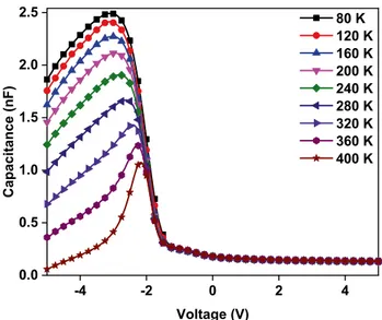
The C–V characteristics of the Au/Cu2WSe4/p-Si devices have been shown in Fig. 2 for various temperatures increas-ing from 80 to 400 K via 40 K steps at 500 kHz frequency. The capacitance values of the device decreased with increas-ing temperature at inversion region and indicated peaks towards depletion region. The peak behavior and shift at the peak positions can be attributed to reordering of the interface states and changes in series resistance [19–22]. However, the capacitance values remained constant at depletion and accumulation regions due to the changes of the temperature and voltage. While the capacitance values decreased with increasing temperature, the peak sharpness increased owing to interface states at the inversion region [23, 24]. Such behavior is hard to find in the literature because generally the capacitance values decrease with decreasing temperature depending on freeze-out effect of the carriers towards low temperatures [25, 26]. This behavior can be attributed to the interfacial layer Cu2WSe4 nanosheets. In addition, the
device has MOS type C–V curves for various temperatures at 500 kHz frequency [23, 27, 28].
The conductance voltage (G–V) plots of the Au/ Cu2WSe4/p-Si heterojunction have been indicated in Fig. 3 in
various temperatures. The G values increased with increas-ing temperature at the inversion region and stayed constant at the depletion and accumulation regions. The increase at the conductance values with increasing temperature can be attributed to increasing mobility of the charge carriers in the interface of the heterojunction device [29]. The increasing temperature also caused peaks for higher temperatures than room temperature. The peaks can be attributed to interface
Fig. 1 The schematic diagram of the Au/Cu2WSe4/p-Si devices
-4 -2 0 2 4 0.0 0.5 1.0 1.5 2.0 2.5 Capacitance (nF) Voltage (V) 80 K 120 K 160 K 200 K 240 K 280 K 320 K 360 K 400 K
Fig. 2 The C–V plots of the Au/Cu2WSe4/p-Si heterojunction for var-ious temperatures
states effect [30]. The peak position changed towards deple-tion region with increasing temperature.
The resistance (Ri) value of the heterojunctions is
inves-tigated to understand the device characteristics better. The resistance of the heterojunction can be calculated from below formula depending on measured capacitance ( Cm )
and conductance ( Cm):
where 𝜔(= 2𝜋f ) is angular frequency. The Ri versus voltage
plots of the Au/Cu2WSe4/p-Si heterojunction have been
indi-cated in Fig. 4 depending on the measurement temperature in the range of 80 and 400 K. According to Fig. 4, the Ri
values are sensitive to the temperature and voltage changes. In other words, the Ri values exhibited peaks at the
inver-sion region and the peak intensity and position increased with increasing temperature and shifted slightly towards the inversion region. The peak behavior of the Ri can be
attributed to that of the trapping charges which have enough energy to escape from the localized traps between the semi-conductor and metal [31–33]. In the accumulation region, the Ri values slightly increased with the increasing
tempera-ture but stayed almost constant via changing the voltage for each temperature.
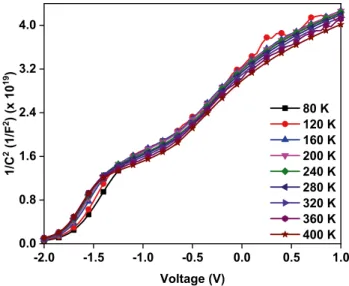
Figure 5 displays the C−2-V graphs of the Au/Cu
2WSe4/p-Si
heterojunction in various temperatures at 500 kHz frequency. The C−2-V plots exhibited almost linearity and parallel to each
other in various temperatures, but there are some deviations from linearity which can be attributed to interfacial Cu2WSe4
nanosheets film layer and non-ideal metal semiconductor structures [34–36]. In addition the non-linear plots of the (1) Ri= Gm G2 m+ ( 𝜔C m )2
C−2-V can be attributed to that of interface states can follow
ac signal at 500 kHz frequency easily [37].
The below formula gives the relation between the capaci-tance and the potential [38]:
where Vd , 𝜀0 , 𝜀s , A , and Na represent diffusion potential,
the permittivity of space, the permittivity of semiconduc-tor, metal contact area and concentration of acceptor atoms, respectively. The Vd is determined in the x-axis
extrapola-tion of the C−2-V plot and the slope of this plot with V
d (2) C−2= 2(Vd+ V ) q𝜀0𝜀sA2Na -4 -2 0 2 4 0 2 4 6 8 10 12 14 16 Conductance (mF/s ) Voltage (V) 80 K 120 K 160 K 200 K 240 K 280 K 320 K 360 K 400 K
Fig. 3 The G–V characteristics of the Au/Cu2WSe4/p-Si heterojunc-tion for various temperatures
-4 -2 0 2 4 0 100 200 300 400 500 Ri (Ω ) Voltage (V) 80 K 120 K 160 K 200 K 240 K 280 K 320 K 360 K 400 K -2.5 -2.0 -1.5 -1.0 100 200 300 400 500 Ri (Ω ) Voltage (V)
Fig. 4 The R–V plots of the Au/Cu2WSe4/p-Si heterojunction for var-ious temperatures -2.0 -1.5 -1.0 -0.5 0.0 0.5 1.0 0.0 0.8 1.6 2.4 3.2 4.0 1/ C 2(1/F 2)( x 10 19) Voltage (V) 80 K 120 K 160 K 200 K 240 K 280 K 320 K 360 K 400 K
Fig. 5 The C−2-V graphs of the Au/Cu
2WSe4/p-Si heterojunction device for various temperatures
helps to determine other parameters such as barrier height (Φb), Fermi energy level (EF), maximum electric field (Em)
and width of the depletion region (Wd). These parameters
were calculated and listed in Table 1 in various tempera-tures. According to Table 1, while the Na , EF, Φb and Em
values increased with increasing temperatures, Wd values
decreased. The increasing at EF values can be attributed to
increasing donor concentrations and charge carriers with the increasing temperature [39]. While the increase at Φb values
can depended on directly increasing diffusion potential, the decrease at the Wd values can be attributed to the increasing
donor concentrations with increasing temperature.
Hill-Coleman technique enables us to determine the inter-face states density (Nss) of the metal–semiconductor
hetero-junctions via the next equation [40]:
(3) Nss= 2 qA (Gm∕𝜔)max ((Gm∕𝜔)maxC0x)2+(1 − Cm∕C0x )2
where C0x is the capacitance of the interfacial layer and
cal-culated with below equation:
In this equation, the Cma and Gma symbolize the
meas-ured capacitance and conductance at accumulation region, respectively. The calculated Nss and Rs values were tabulated
in Table 1 in various temperatures.
Figure 6a, b shows the temperature dependent profile of the Nss, Φb and Na , Rs. According to Fig. 6, while the Nss,
Φb and Na values increased with increasing temperature, the
Rs values increased up to 240 K and then slightly decreased
towards 400 K. This can be attributed to the semiconductor properties of the Cu2WSe4 nanosheets interfacial layer.
To remove the series resistance effects of the device, the interface states, the capacitance and conductance values (4) C0x= Cma [ G2 ma ( 𝜔Cma )2 ]
Table 1 The temperature dependent electrical parameters of the Au/Cu2WSe4/p-Si heterojunction device calculated form the C−2-V graphs f (kHz) Na (1016 cm−3) Vi (V) EF (meV) Φb (eV) Em (104 V/m) Wd (10−5 cm) Nss (eV−1 cm−2) Rs (Ω)
80 1.18 1.96 0.036 1.97 8.38 4.68 2.94 × 10⁹ 55.5 120 1.19 1.99 0.053 2.02 8.46 4.70 6.17 × 10⁹ 62.2 160 1.25 2.06 0.071 2.11 8.85 4.68 6.33 × 10⁹ 69.7 200 1.27 2.09 0.088 2.16 9.00 4.67 8.04 × 10⁹ 74.2 240 1.30 2.11 0.105 2.20 9.12 4.64 1.07 × 10¹⁰ 75.4 280 1.33 2.12 0.122 2.23 9.24 4.61 1.31 × 10¹⁰ 73.5 320 1.36 2.13 0.139 2.26 9.36 4.58 1.58 × 10¹⁰ 68.8 360 1.37 2.12 0.156 2.27 9.41 4.54 1.99 × 10¹⁰ 63.5 400 1.40 2.13 0.172 2.31 9.54 4.51 2.28 × 10¹⁰ 60.0 100 150 200 250 300 350 400 2.00 2.08 2.16 2.24 2.32 Temperature (K)
Barrier Height (eV)
(a)
0.0 0.5 1.0 1.5 2.0 2.5 Nss (e V -1.c m -2) x 10 10 100 150 200 250 300 350 400 1.15 1.20 1.25 1.30 1.35 1.40(b)
Temperature (K) Na (c m -3) x 10 16 50 55 60 65 70 75 Rs (Ω )should be corrected [41]. The adjusted capacitance and con-ductance values are calculated in below equations:
where 𝛼 is given by the following equation:
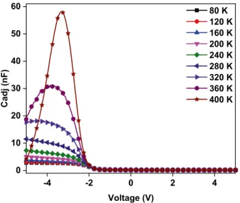
Figure 7 indicates Cadj versus voltage plots of the Au/
Cu2WSe4/p-Si heterojunction device in various
tempera-tures. The corrected capacitance values increased with increasing temperature and exhibited peaks at the inversion region. The peak property of the capacitance values can be attributed to interface states [42]. There are no changes at the capacitance values in the depletion and accumulation region with the temperature and voltage changes.
The Gadj versus voltage plots of the Au/Cu2WSe4/p-Si
heterojunction have been shown in Fig. 8 in various tem-peratures. The corrected conductance values increased with increasing temperature and exhibited peaks towards the higher temperature and inversion region. The peak behav-ior at the conductance values can be attributed to interface states effect via changing temperature [43]. The Gadj did not change at the depletion and accumulation region via the changing temperature and voltage.
(5) Cadj= [ G2m+( 𝜔Cm)2 ( 𝜔Cm )2 + 𝛼2 ] Cm (6) Gadj= [ G2m+( 𝜔Cm)2 ( 𝜔Cm )2 + 𝛼2 ] 𝛼 (7) 𝛼= Gm− [ G2m+( 𝜔Cm)2 ] Rs
4 Conclusion
The Cu2WSe4 nanosheets were fabricated by hot-injection
method and deposited between the metal and p-Si by spin coating technique to obtain Au/Cu2WSe4/p-Si heterojunc-tion device. The obtained device was characterized by C–V and G–V measurements in various temperatures from 80 to 400 K by 40 K steps at 500 kHz frequency. The C–V and
G–V characteristic of the Au/Cu2WSe4/p-Si heterojunc-tion device exhibited peaks at the inversion region and did not change at the depletion and accumulation region. The peak behavior of the device in various temperatures was attributed to interface states and series resistance. The Au/ Cu2WSe4/p-Si heterojunction device has MOS type C–V
curves. The resistance values of the device are sensitive to temperature and voltage changes. The electrical param-eters such as EF, Φb, Em and Wd were calculated by the
C−2-V plots and discussed in details depending on the
tem-perature changes. The corrected capacitance and conduct-ance values were calculated to see interface states effect on the device. The Cu2WSe4 nanosheets can be used in capacitor application as an interfacial layer in the industry.
Acknowledgements The authors would like to thank to Selçuk University BAP office (Project Number 17401159) and Karamano-glu Mehmetbey University (Grand Number: 32-M-16) for Scientific Research Foundation. -4 -2 0 2 4 0 10 20 30 40 50 60 Cadj (nF) Voltage (V) 80 K 120 K 160 K 200 K 240 K 280 K 320 K 360 K 400 K
Fig. 7 Cadj-V plots of the Au/Cu2WSe4/p-Si heterojunction device in various temperatures -4 -2 0 2 4 0 20 40 60 80 100 120 140 160 180 Gadj (mF/s) Voltage (V) 80 K 120 K 160 K 200 K 240 K 280 K 320 K 360 K 400 K -5 -4 -3 -2 -1 0.000 0.005 0.010 0.015 Gadj (mF/s) Voltage (V)
Fig. 8 Gadj-V plots of the Au/Cu2WSe4/p-Si heterojunction device in various temperatures
References
1. V. Sousa, Chalcogenide materials and their application to non-volatile memories. Microelectron. Eng. 88, 807–813 (2011). https ://doi.org/10.1016/j.mee.2010.06.042
2. P. Lucas, B. Bureau, Selenide glass fibers for biochemical infrared sensing, in Applications of chalcogenides S, Se, Te, ed. by G.K. Ahluwalia (Springer International Publishing, Cham, 2017), pp. 285–319
3. J. Troles, L. Brilland, Chalcogenide microstructured optical fibers for infrared applications, in Chalcogenide glasses, 1st edn., ed. by J.-L. Adam, X. Zhang (Woodhead Publishing, Cam-bridge, 2013), pp. 411–437
4. G. Kaur Ahluwalia (ed.), Applications of chalcogenides: S, Se, and Te, 1st edn. (Springer International Publishing, Cham, 2017)
5. Y. Kim, A.P. Tiwari, O. Prakash, H. Lee, Activation of ternary transition metal chalcogenide basal planes through chemical strain for the hydrogen evolution reaction. ChemPlusChem 82, 1166 (2017). https ://doi.org/10.1002/cplu.20170 0247
6. A.P. Tiwari, D. Kim, Y. Kim, O. Prakash, H. Lee, Highly active and stable layered ternary transition metal chalcogenide for hydrogen evolution reaction. Nano Energy 28, 366–372 (2016). https ://doi.org/10.1016/j.nanoe n.2016.08.065
7. J. Liu, H. Wang, C. Fang, L. Fu, X. Qian, Van der waals stack-ing-induced topological phase transition in layered ternary transition metal chalcogenides. Nano Lett. 17, 467–475 (2017). https ://doi.org/10.1021/acs.nanol ett.6b044 87
8. A. Wold, K. Dwight, Ternary transition metal chalcogenides AB2X4, Solid state chemistry (Springer, Dordrecht, 1993), pp. 222–235
9. W. Chen, H. Chen, H. Zhu, Q. Gao, J. Luo, Y. Wang, S. Zhang, K. Zhang, C. Wang, Y. Xiong, Y. Wu, X. Zheng, W. Chu, L. Song, Z. Wu, Solvothermal synthesis of ternary Cu2MoS4 nanosheets: structural characterization at the atomic level. Small
10, 4637–4644 (2014). https ://doi.org/10.1002/smll.20140 0752 10. A. Kagkoura, T. Skaltsas, N. Tagmatarchis, Transition-metal
chalcogenide/graphene ensembles for light-induced energy applications. Chem. A 23, 12967–12979 (2017). https ://doi. org/10.1002/chem.20170 0242
11. S. Zheng, L. Sun, T. Yin, A.M. Dubrovkin, F. Liu, Z. Liu, Z.X. Shen, H.J. Fan, Monolayers of WxMo1-xS2alloy heterostructure with in-plane composition variations. Appl. Phys. Lett. 106, 063113 (2015). https ://doi.org/10.1063/1.49082 56
12. S.D. Karande, N. Kaushik, D.S. Narang, D. Late, S. Lodha, Thickness tunable transport in alloyed WSSe field effect tran-sistors. Appl. Phys. Lett. 109, 142101 (2016). https ://doi. org/10.1063/1.49642 89
13. A. Sarilmaz, M. Can, F. Ozel, Ternary copper tungsten sele-nide nanosheets synthesized by a facile hot-injection method. J. Alloys Compd. 699, 479–483 (2017). https ://doi.org/10.1016/j. jallc om.2016.12.401
14. A. Kocyigit, M. Yıldırım, A. Sarılmaz, F. Ozel, The Au/ Cu2WSe4/p-Si photodiode: electrical and morphological char-acterization. J. Alloys Compd. 780, 186–192 (2019). https ://doi. org/10.1016/j.jallc om.2018.11.372
15. M. Yıldırım, A. Sarılmaz, F. Özel, Investigation of optical and device parameters of colloidal copper tungsten selenide ter-nary nanosheets. J. Mater. Sci. 29, 762–770 (2018). https ://doi. org/10.1007/s1085 4-017-7970-7
16. İ. Yücedağ, A. Kaya, H. Tecimer, Ş. Altındal, Temperature and voltage dependences of dielectric properties and ac electrical conductivity in Au/PVC + TCNQ/p-Si structures. Mater. Sci. Semicond. Process. 28, 37–42 (2014). https ://doi.org/10.1016/j. mssp.2014.03.051
17. Ş. Aydoğan, M.L. Grilli, M. Yilmaz, Z. Çaldiran, H. Kaçuş, A facile growth of spray based ZnO films and device performance investigation for Schottky diodes: determination of interface state density distribution. J. Alloys Compd. 708, 55–66 (2017). https ://doi.org/10.1016/j.jallc om.2017.02.198
18. H. Matsushita, Y. Tojo, T. Takizawa, Schottky properties of CuInSe2 single crystals grown by the horizontal Bridgman method with controlling Se vapor pressure. J. Phys. Chem. Solids 64, 1825–1829 (2003). https ://doi.org/10.1016/S0022 -3697(03)00247 -6
19. D. Korucu, Ş. Altindal, T.S. Mammadov, S. Özçelik, On the temperature dependent anomalous peak and negative capaci-tance in Au/n-InP schottky barrier diodes. Optoelectron. Adv. Mater. Rapid Commun. 3, 56–59 (2009)
20. S. Stemmer, V. Chobpattana, S. Rajan, Frequency dispersion in III-V metal-oxide-semiconductor capacitors. Appl. Phys. Lett.
100, 233510 (2012). https ://doi.org/10.1063/1.47243 30 21. İ. Orak, The performances photodiode and diode of ZnO thin
film by atomic layer deposition technique. Solid State Commun.
247, 17–22 (2016). https ://doi.org/10.1016/j.ssc.2016.08.004 22. Ö. Vural, Y. Şafak, A. Türüt, Ş. Altındal, Temperature
depend-ent negative capacitance behavior of Al/rhodamine-101/n-GaAs Schottky barrier diodes and Rs effects on the C–V and G/ω–V characteristics. J. Alloys Compd. 513, 107–111 (2012). https :// doi.org/10.1016/j.jallc om.2011.09.101
23. S. Demirezen, Ş. Altindal, On the temperature dependent pro-file of interface states and series resistance characteristics in (Ni/Au)/Al0.22Ga0.78N/AlN/GaN heterostructures. Phys. B 405, 1130–1138 (2010). https ://doi.org/10.1016/j.physb .2009.11.015 24. E. Arslan, Y. Şafak, Ş. Altındal, Ö. Kelekçi, E. Özbay, Ş. Altin-dal, Ö. Kelekçi, E. Özbay, Temperature dependent negative capacitance behavior in (Ni/Au)/AlGaN/AlN/GaN heterostruc-tures. J. Non-Cryst. Solids 356, 1006–1011 (2010). https ://doi. org/10.1016/j.jnonc rysol .2010.01.024
25. S. Duman, E. Gür, S. Doğan, S. Tüzemen, Temperature depend-ent capacitance and DLTS studies of Ni/n-type 6H-SiC Schottky diode. Curr. Appl. Phys. 9, 1181–1185 (2009). https ://doi. org/10.1016/j.cap.2009.01.009
26. D.E. Yildiz, Ş. Altindal, H. Kanbur, Gaussian distribution of inhomogeneous barrier height in Al/SiO2/p-Si Schottky diodes. J. Appl. Phys. 103, 124502 (2008). https ://doi. org/10.1063/1.29369 63
27. X. Zou, G. Fang, J. Wan, X. He, H. Wang, N. Liu, H. Long, X. Zhao, Improved subthreshold swing and gate-bias stressing stability of p-type Cu2O thin-film transistors using a Hfo2high-k gate dielectric grown on a SiO2/Si substrate by pulsed laser ablation. IEEE Trans. Electron Devices 58, 2003–2007 (2011). https ://doi.org/10.1109/TED.2011.21423 13
28. G. Conibeer, I. Perez-Wurfl, X. Hao, D. Di, D. Lin, Si solid-state quantum dot-based materials for tandem solar cells. Nanoscale Res. Lett. 7, 193 (2012). https ://doi. org/10.1186/1556-276X-7-193
29. A. Gümüş, G. Ersöz, İ. Yücedağ, S. Bayrakdar, Ş. Altindal, Comparative study of the temperature-dependent dielectric prop-erties of Au/PPy/n-Si (MPS)-type Schottky barrier diodes. J. Korean Phys. Soc. 67, 889–895 (2015). https ://doi.org/10.3938/ jkps.67.889
30. M. Yildirim, P. Durmuş, Ş. Altindal, Analyses of temperature-dependent interface states, series resistances, and AC electrical conductivities of Al/p—Si and Al/Bi4Ti 3O12/p—Si structures by using the admittance spectroscopy method. Chin. Phys. B 22, 108502 (2013). https ://doi.org/10.1088/1674-1056/22/10/10850 2 31. İ. Yücedağ, A. Kaya, Ş. Altındal, I. Uslu, Frequency and voltage-dependent electrical and dielectric properties of Al/Co-doped PVA/p-Si structures at room temperature. Chin. Phys. B 23, 047304 (2014). https ://doi.org/10.1088/1674-1056/23/4/04730 4
32. İ. Dökme, Ş. Altındal, T. Tunç, İ. Uslu, Temperature depend-ent electrical and dielectric properties of Au/polyvinyl alcohol (Ni, Zn-doped)/n-Si Schottky diodes. Microelectron. Reliab. 50, 39–44 (2010). https ://doi.org/10.1016/J.MICRO REL.2009.09.005 33. M.M. Bülbül, S. Zeyrek, Ş. Altındal, H. Yüzer, On the profile of
temperature dependent series resistance in Al/Si3N4/p-Si (MIS) Schottky diodes. Microelectron. Eng. 83, 577–581 (2006). https ://doi.org/10.1016/j.mee.2005.12.013
34. Ç. Bilkan, Ş. Altındal, Y. Azizian-Kalandaragh, Investigation of frequency and voltage dependence surface states and series resistance profiles using admittance measurements in Al/p-Si with Co3O4-PVA interlayer structures. Phys. B 515, 28–33 (2017). https ://doi.org/10.1016/J.PHYSB .2017.04.002
35. I. Orak, A. Kocyigit, I. Karteri, S. Uruş, Frequency-dependent electrical characterization of GO-SiO2 composites in a Schottky device. J. Electron. Mater. 47, 6691–6700 (2018). https ://doi. org/10.1007/s1166 4-018-6571-4
36. J. Szatkowski, K. Sierański, Simple interface-layer model for the nonideal characteristics of the Schottky-barrier diode. Solid State Electron. 35, 1013–1015 (1992). https ://doi.org/10.1016/0038-1101(92)90333 -8
37. M.M. Bülbül, S. Bengi, I. Dökme, S. Altındal, T. Tunç, Tempera-ture dependent capacitance and conductance-voltage character-istics of Au/polyvinyl alcohol(Co, Zn)/n-Si Schottky diodes. J. Appl. Phys. 108, 034517 (2010). https ://doi.org/10.1063/1.34624 27
38. S.M. Sze, Physics of semiconductor devices, 2nd edn. (Wiley, NewYork, 1981)
39. Ş. Aydoǧan, M. Saǧlam, A. Türüt, The effects of the tempera-ture on the some parameters obtained from current-voltage and
capacitance-voltage characteristics of polypyrrole/n-Si structure. Polymer (Guildf) 46, 563–568 (2005). https ://doi.org/10.1016/j. polym er.2004.11.006
40. Ç. Bilkan, A. Gümüş, Ş. Altındal, The source of negative capaci-tance and anomalous peak in the forward bias capacicapaci-tance- capacitance-voltage in Cr/p-si Schottky barrier diodes (SBDs). Mater. Sci. Semicond. Process. 39, 484–491 (2015). https ://doi.org/10.1016/j. mssp.2015.05.044
41. A. Turut, A. Karabulut, K. Ejderha, N. Bıyıklı, Capacitance– conductance–current–voltage characteristics of atomic layer deposited Au/Ti/Al2O3/n-GaAs MIS structures. Mater. Sci. Sem-icond. Process. 39, 400–407 (2015). https ://doi.org/10.1016/j. mssp.2015.05.025
42. I.S. Yahia, M. Fadel, G.B. Sakr, S.S. Shenouda, F. Yakuphanoglu, Effect of the frequency and temperature on the complex imped-ance spectroscopy (C–V and G-V) of p-ZnGa2Se4/n-Si nanostruc-ture heterojunction diode. J. Mater. Sci. 47, 1719–1728 (2012). https ://doi.org/10.1007/s1085 3-011-5951-4
43. Y. Şafak-Asar, T.T. Asar, Ş. Altındal, S. Özçelik, Ş. Altindal, S. Özçelik, Investigation of dielectric relaxation and ac elec-trical conductivity using impedance spectroscopy method in (AuZn)/TiO2/p-GaAs(1 1 0) schottky barrier diodes. J. Alloys Compd. 628, 442–449 (2015). https ://doi.org/10.1016/j.jallc om.2014.12.170
Publisher’s Note Springer Nature remains neutral with regard to jurisdictional claims in published maps and institutional affiliations.