See discussions, stats, and author profiles for this publication at: https://www.researchgate.net/publication/3525723
Capacitively coupled converter (C3) for high power DC-DC conversion
Conference Paper · July 1991DOI: 10.1109/PESC.1991.162647 · Source: IEEE Xplore
CITATIONS 6
READS 16 3 authors, including:
Some of the authors of this publication are also working on these related projects: physical, mechanical and electrical properties of epoxy nano compositView project
Space Power SystemsView project Morteza Ehsani
Iran Polymer and Petrochemical Institute 249PUBLICATIONS 5,589CITATIONS
SEE PROFILE
Mehmet Oruç Bilgiç T.C. Istanbul Kultur University 17PUBLICATIONS 126CITATIONS
SEE PROFILE
All content following this page was uploaded by Mehmet Oruç Bilgiç on 08 May 2017. The user has requested enhancement of the downloaded file.
C A P A C I T I V E L Y C O U P L E D C O N V E R T E R ( C 3 )
FOR HIGH POWER D C - D C C O N V E R S I O N
M.
Ehsanz M . O . U71gaGS.
KhanPower Electronics Laboratory Department of Electrical Engineering
Texas A
9i
M University College Stat,ion, TX. 77843-3128 A b s t r a c tThe Capacitive Coupled Converter (C3) is described for high power voltage source dc-dc applications. Its steady-state and dynamic behavior are analysed theoretically and by com- puter simulation. Factors affecting its operation and control are discussed and some design rules are presented. A proof of principle model of C3 was constructed and its waveforms were recorded.
1. I n t r o d u c t i o n
A schematic diagram of the Capacitive Coupled Converter (
C3 ) is shown in Fig. 1. The basic concept of this converter was proposed by Simon And Bronner of Princeton Plasma Physics Laboratoryjn 1967 (11. This converter concept was specifically intended for high power energy transfer between two current sources (two large inductors). However, they suggested igni- trons for switching elements. The first experimental capacitive fly-back converter circuit
,
using SCRs for power switches, was proposed by Dick and Dustman (21.In Fig. 1. we present a modification of Simon and Bron- ner’s converter concept which is appropriate for voltage source dc-dc high power processing. A low power variation of this cir- cuit which uses a high frequency transistor for
S
I
and a diode for Sz has also been presented under the the name Citk con- verter [3].However, the hard current turn-off nature of switch SIin that converter makes it inappropriate for high power a.pplica- tions. Our proposed Capacitor Coupled Converter uses capaci- tive commutation of both
SI
and Sz switches. Therefore, SCRscan be used to implement these switches and the power capa- bility of the converter can be expanded by orders of magnitude. If a high frequency design is required to reduce reactive clement sizes, then high power gate turn-off devices, such as the GTO,
ZTO or MCT can be used. Since these devices will have to switch at zero current (subsequent to capa.citive commutation ),
their switching losses and switching speeds can be significa.ntly improved beyond the common applications of these devices. Fur- thermore, the symmetrical topology of our proposed converter, makes it bilateral (two-quadrant) power converter and regener- ated load energy can be transferred to the source. Note that
C3
is both a voltage step-up and step-down converter and can be controlled in both zones.2. P r i n c i p l e of O p e r a t i o n
The operation of C3 circiiit during a t,ypical cycle is a s fol- lows. When
SI
is conducting a.nd 5’2 is not, the capacitor, C1,is being chargcd from or discharged into the load side inductor,
Lz, depending on the polarity of its initial cha.rge. At t,he sa.me time, current in Ll is being conducted through
SI.
WhenSz
is conducting and S1 is not, the capacitor is being charged from or discharged into the source side inductor, L1, depending on the initial charge on the ca.pacitor. At the sa.me time the load side inductor current is being conducted through 5’2. The voltagewaveforms for a typical cycle with 1 1
>
I2 are shown in Fig. 2. By proper design of the induct,ors and frequency,
continu-ous current is maintained in both L1 and Lz, over a switching period. The coupling capacitor, C1, voltage waveform is a com- bination of charging by currents Il and Iz. The negative slope corresponds to the interval when SI is conducting and the load side current, 12, discharges the capacitor from +V, to -Vm. The positivo slop corresponds to the interval when
Sz
is conducting and the source side current, 11, charges the ca.pa.citor from -I<,,to +V,. Not,e that the coupling c a p c i t o r volta.ge is made to al-
ternat,e in polarity so that both 5’1 a.nd Sz ca.n be commutated. However, for efficient energy transfer, this capacitor is highly biased to one side. To summarize, in a typical converter cycle a.
small amount of source energy is transferred to the source
Figure 1 : Schematic of capacitor coupled converter.
vn vo
Figure 2 : Volta.ge wavefornls for capacitive coupled con- verter (C’) when I ,
>
I z .inductor, L1, (Si is on) and the same amount of energy is trans-
ferred from capa.citor, C1, to the load side. In the next subcycle
(S2 is on), the small amollnt of sollrce inductor excess energy is
transferred to the capacitor GI, while some of the load inductor excess energy is transferred to the 1oa.d capacitor, Cz, and R.
Therefore, the capacitor, Cl serves two funct,ions. One as inter-
medin.te energy biiffer and the 0thr.r as a commutation capacitor. For a low input-nut.put nirrent ripple operation the capa.citor,
C1, energy is nnich smallrr than t,he inductive energy in Li and
Lz a.nd t,his is ensured b y design. Power and voltage control is achieved by varying the converter operating period and the peak voltages of C1 within one period. Several operating and control methods are possible as discussed in references (41 a.nd [5].
Other variations of the basic Capacitive Fly-back Converter have been studied in [6,7] for high power and [8] for low power.
0-7803-0090-4/91/0707$01.00 01991IEEE
-Figure 3: Schematic of the Dual Capacitive Coupled Con-
verter Circuit.
For example, Figure 3. shows the schematic of a dual capacitive coupled converter which helps reduce the input-output current ripple and provides more degrees of freedom in control.
3. Analysis of S t e a d y - S t a t e O p e r a t i o n
threr conditions must be satisfied. equal to the input voltage.
To obtain a stable operation in steady-state the following
1 - The average of the voltage across 5’1,
<
u,1>,
must be<
V J 1>=
Vl (1)2 - The average of the voltage across the S Z ,
<
713.2>,
mustbe equal to the output voltage
<
V,2>=
vz
(2)3 - The rate of energy transferred by the capacitor C1 must
be equal to the rate of the energy consumed by the load R.
(3) where V, is the positive peak value of the capacitor C1 voltage and V,,, is the negative peak, as shown in 0,1 of Fig. 2, a.nd T is
the switching period.
These three conditions can also be formulated as follows.
(4)
(6) 2RC1 G2 V, - V,,
-- -
T (1
+
G ) 2 V,+
V, where G is the voltage gain (V2/&).4. Design of C3
To guarantee commutation in the loop consisting of SI - C1
-
Sz, in Figure l., V, must be set by design. SimilarIy, to guaratee over voltage protection of the switches, V, is also set by design. For the rated or nominal operating conditions VI, Vz andR are given. For a given voltage gain, G = Vz/Vl, in cquation
(6), we can set the value of the coupling capacitor, C1, to get the period, T, which is within the switching speed rating and acceptable input/output filter design sizing to meet the ripple specs. For steady state nominal operation the coupling capacitor voltage threshold comparator is set at V,, and V, and this will also guaratee all of the above considerations.
Control o f C 3
Two variables may cause small signal perturbation around the steady state operating point:
1- Load changes from R I to R2 ( Regulation): By keeping V, and V, constant the gain, G, is kept constant from expression
(4). This means that V2 is also constant (G = V*/Vl) and the
I
I
7
small change of load R is corrected by a small changes of period T , according to equation (6 . As long as change of R is small, on the input-output filter effectiveness and the resulting ripples. 2- Change of gain, G ( Control): Suppose VI is constant and V2 must change to 1/21 which is close to Vz. The following equation can be obtained from equations (4) and (5)
change of T will be small an
d
this slioiild not have a large impactIn this equation, it is seen tha.t Vn, can be kept constant to
guaratee commutation and V, is changed to accomodate the new gain. This will ca.usC small modiilation of period T a.s in the previous case.
The dynamics of the above small signal control ca.n be anal- ysed from average models which are similar to those a1rea.dy developed for this converter topology [3]. However, here the switching period is not constant, but changes in the small.
Large control transients ca.n lie handled by large signal coii- trol. An example is startbup transient where the gain goes from zero to a finite number siich a.s 3. From equation (8) i t is ob- served that if VI and V,, are constant a large change in V2;
e.g., from zero to Vz,will requirc a large cha.nge in V, (from zero to Vo). However, the input resonant loop consisting of VI - L1 - C1 - 5’1 puts a theoretical limit on the largest V, achievable in any one switching cycle. For example, for the first start-up switching cycle, this limit is approximately
V O I L 1’1. (9)
where V,, is the maximum obtainable voltage in the first res- onant cycle, which is ideally eqiial to 2Vl. If this V,, is much smaller than the steady state V, than several cycles of start-up
transients are required, cach one ta.king a.dvantage of the largest growth in V, that can be achieved in one cycle, so that the steady state is reached in the shortest tra.nsient time. However, this then requires a set of transient V, commmds to be fed to the threshold compa.rator of the coupling capacitor voltage. The steps of V, to be fed to the comparator depend on the C3 circuit
dynamics a.nd can only be derived by siinulation or cycle to cy- cle circuit malysis. This dynamic behavior ca.nnot be predicted from the previously mentioned small signal avera.ge model a.nd must be obta.ined from act,ua.l C 3 circuit including its para.sitic resishnces, etc. The rea.son is that the switching period is al- lowed to change widely over a short time.
Design Example
In the following a non optimized design exa.mple will be pre- sented for illustration. The C 3 to he designed has the following specifications.
Input voltage, VI =‘2TOV Output voltage, V2 = 28V Output Power P, = 251i‘W Switching Frequency, f, = 501CHz Gain, G = 0.104.
The load resistance will be R = \?/P ,.I = 28’/25 x lo3 =
0.0314ohnzs capacitor, C1, is
Assuming V,/V, = 0.1
,
from equation (6) the couplingT GZ V, - V ,
c1
= - _ _ _ ~2R
(1+
G)2 V,+
V, 20 x 0.104’ 1 - 0.1 2 x 0.0314 ( 1+
0.104)2 1+
0.1 -- - = 2.31 x lo-‘ F = 2.31 /rFFroin equa.tion (4) and lfo/V,,, = 0.1, V, and V,,, are FG2 V
L1 and L2 can be found for a. given set of AI1 and AI2 and 66.2 V, respect,ively.
currpnt ripples by the following approsima.te formulas.
(9) 28
(Vo - Vz)'T G 2A12(Vo
+
V,,,)(=)Lz
=For 20% and 40% input and output current, ripple, respec- Similarly, t,he output filter capacitor can be found from tively,
L1
= 0.1 mH andLz
= 1.6 p H .AI2.T
c2= -
8AV2
'
where AV2 is the given peak-to-peak output voltage ripple. For
4% output voltage ripple, Cz is 800 pF.
5. Simulation Results
A computer model was developed for simulation which was based on the switched converter topology. Runga-Kutta method was used to perform the solution of the circuit equations.
Figures 4,5 and 6 show the simulation results for the C3
which was designed in the previous section.
time (msecs)
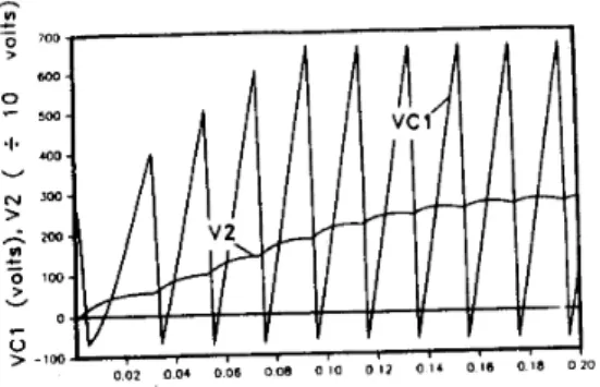
Figure 5 : Large signal start-up transient of coupling ca- pacitor voltage, v C l and output voltage, vz.
Figure 4: Small signal transient of coupling capacitor volt- age, vel, and output voltage, v e l , due t o gain change.
.
, . ,-100 c
b,
O b 5 0'10 0 ; 5 0 ; O O i 5 O!O Figure 6 : Small signal transient of coupling capacitor volt- a.ge, vel, and output voltage due to load cha.nge.Figure 7: The experimental capacitor coupled converter.
.
....
,(d)
Figure 8 : Experimental waveforms of the C 3 . a) Input current 2.5 A/div. b)Output inductor current, 2.5 A/div., c) The coupling capacitor voltage, 50 V/div., d ) Output voltage 2.5 V/div. Time scale: 100 ps. Oscillograms are taken for
I , = 6 A, I2 = 4.8 A and G=1.13.
6. Experimental Results
A small exprimental C 3 was built for proof of principle in the Power Electronics Laboratory a.t Texas A&M University. This circuit and its component va.lues are shown in Figure 7. The experimental waveforms a.re seen in Figure 8.
7. Conclusions ,
The G 3 circuit for high power DC-DC voltage source appli- cation is presented in this paper. This converter has been de- rived from the Single Flying Capa.citor Converter, SFC, which was used in superconductive energy storage magnets (1,2]. The capacitor coupled converter is capable of controlled step-up and step-down cont,rol withorit the need of transformer. The combi- nation of C3’s inherent current commutation and gate turn-off
devices can l e a d to efficient, high frequency, high power (de- termined by the available switching devices ) converters
,
with compact filters. The use of SCR’s as the switching elements can lead t o C 3 designs with virtually unlimited power capabilities.Acknowledgement
Shoen in the experimental phase of this work. 8. References
[l] E.D. Simon a.nd Bronner, ”An Inductive Energy Storage System Using Ignitron Switching,” I E E E Tmns. o n Nuclear Science, Vol. NS-14, No. 5, Oct. 1?,67.
12) E.P. Dick a.nd Dustman, Inductive Energy Transfer Using a Flying C‘npacitor,” Energy Stornge, Com,pression and
Switchina. book. Edit,ed bv W.H. Bostick. V. Na.rdi a.nd O.S.F.
T h e authors greatfully a.cknow1edge the assistance of Mike
Zucker, f’lenum’Press, New York, 1976.
itk and R.D. Middlebrook,” A New Optimum Topol- ogy fA;i$ng DC- to-DC Convertcr,” I E E E Power Electron& Speciahts Conference I h ” i S , ’ ’ pp. 160-179, 1977.
141 M. Ehsani and R.L. I<rtstom. converter Circuits for ’
Siipekc‘onductive Ma.gnetic Energy Storage, Texas A&M Priss, 1988.
(51 M.O. BiIgis and M. Ehsani, ”Analysis of Single Flying Capacitor Converter by the State-Space Averaging Technique,”
I E E E International Symposium, o n Circit.its an’d System,J Pro- ceedings, pp. 1151- 1154, 1989.
16) M.O. Bilgiq and M. Ehsani, ” Time Averaged Behaviors
of Single and Dual Flying Capacitor Converters”, International .Toumal of Electronics, Vol. 66, pp. 655-663, 1989.
(71 M.Ehsani, A. Hozabri and R.L. Kustom, ”Decoupled Control Techniques for Dual Flying Capacitor Bridge Power Supplies for Large Supercondactive Magnets”, I E E E Trans. o n
Magnetics, Vol. MAG-23, No. 2, 1987.
18) S. Citk and R.D. Middlebrook, ”Coupled Inductor and Other Extensions of a New Optimum Topology Switching DC- to-DC Converter,” I E E E Indaslry Application Society Annual
Meeting, pp. 1110-1126, 1977.
30
I- 1
View publication stats View publication stats