Determination of Contact Parameters of Au/n-Ge
Schottky Barrier Diode with Rubrene Interlayer
Murat YILDIRIM*
Department of Biotechnology, Faculty of Science, Selçuk University, Konya, Turkey ( Received : 01.04.2016 ; Accepted: 25.04.2016 )
ABSTRACT
Electrical characterization of an Au/n-Ge semiconductor Schottky diode with organic (rubrene) interface has been systematically carried out over a wide temperature range. In sample fabrication stage, first, the ohmic In contact has been performed on one surface of n-Ge wafer grown in direction of (100). Later, the other surface of the wafer has been coated with rubrene by spin-coating method and then the Schottky contact has been constituted on the organic material via thermal evaporation method. The current-voltage (I-V) characteristics of prepared Schottky diode has been measured at a temperature range of 150-300 K and it has been observed that the diode have a rather good rectification behavior at all temperature. By using the I-V characteristics, the idealite factor, barrier height and some other diode parameters have been calculated for all temperatures. These parameters have also been calculated by means of Cheung-Cheung method. Werner and Güttler’s model has been employed to analyze the temperature dependence of barrier height and ideality factor at low temperatures. The standard deviation of the zero-bias barrier height was calculated as 120 mV and the voltage coefficients of the barrier height were determined as 𝜌2 = 0.184 and 𝜌3 = 0.232 mV. At high temperatures, the zero-bias barrier height decreases with increasing temperature because of the temperature dependence of semiconductor band gap. The non-linearity has been observed in the Richardson plot due to temperature dependence of the zero-bias barrier height. Richardson constant was determined by using different methods. Of the current-voltage analysis’s has emerged an abnormal decrease of apparent barrier height and increase of ideality factor at low temperature. It is determined that these abnormalies result due to the barrier height inhomogeneities prevailing at the organic-semiconductor interface. As a result, homogeneities in Au/rubrene/n-Ge Schottky barrier diode can be successfully characterized by a Gaussian distribution.
Key words: Schottky Contacts, Rubrene Thin Film, Gaussian Distribution, Inhomogeneities.
1. INTRODUCTION
Electronic devices that are created on organic semiconductors are included in the field of organic electronics, and it has progressed at a rapid pace, and electronics based on organic thin-film materials could soon become a backbone of semiconductor technology. The performance of organic semiconductors is mainly connected to their molecular packing which contains the definitions of surfactant tail volume, tail length and equilibrium area per molecule, crystallinity which is the degree of structural order in a material, growth mode, and purity [1]. Holes and electrons in p orbitals are the typical charge carriers inorganic semiconductors. When our daily lives are considered, it is an undeniable fact that electronic devices are and will be an indispensable part of our lives. Semiconductor based materials are used in many of these devices which have been a permanent part of our lives. Among these, Schottky diodes produced by combining a metal and semiconductor material appear to be an indispensable item in the world of electronics together with big developments in the field of semiconductor based technologies and vacuum technology. When the fields in which these devices are used considered, we face with an extent whose borders are vague. Charge transport typically relies on the ability of the charge carriers to move from one molecule to another, which depends on the energy gap between
HOMO which is the highest occupied molecular orbital and LUMO which is the lowest unoccupied molecular orbital levels. The conduction band and the valance band are usually replaced by the LUMO and the HOMO, respectively. Especially in amorphous layers of organic semiconductor the density of states (DOS) is quite well represented by a Gaussian-like distribution of localized molecular orbitals of individual molecules [2]. These materials are either based on oligomers such as pentacene, anthracene, rubrene, or oligothiophenes, or on polymers such as polypyrrole, polyacetylene, poly(3-hexylthiophene)(P3HT), or poly(p-phenylene vinylene) (PPV) [3]. Djurovich et al. [4] have been presented the interrelationships between the LUMO energies of a variety of organic semiconductors measured by several techniques. These correlations allow us to evaluate the accuracies and advantages of the various methods, and to extract a relationship between the exciton binding energy and the energy gap.
Organic semiconductors have attracted much attention because of their fundamental scientific importance and impressive improvements in performance in a wide variety of commercial products based on organic light emitting diodes (OLEDs), organic photovoltaic cells (OPV) and organic field-effect transistors (OFETs) have entered the market. The future may see an even wider range of application for this technology [5]. One specific area that organic semiconductors is Schottky Barrier Diode application. The choice of the material that will be used in Schottky diode should be compatible with the conditions of the diode’s scope of application. The fact *Sorumlu Yazar (Corresponding Author)
e-posta: [email protected]
that germanium semiconductor has high electron mobility has caused it to be used commonly in high frequency applications. It is a great issue of interest to thoroughly comprehend the nature of the electrical characteristics of Schottky diode due to their technological importance. This point is of remarkable significance in terms of the fact that the produced circuit part should serve fort the desired purpose. Moreover, knowing the behavior of produced diodes against sample temperature is an desideratum fort them to operate in harmony with the temperature conditions to which application scopes depend on. Some certain operations have been carried out in order to obtain high quality productivity from Schottky diodes. Of these operations, the annealing process appears to be as an effect to increase the diode quality significantly. When this feature is considered, the effect of annealing temperature and how the annealing temperatures affect various features of the diode and resulting from this how the electronic features change are becoming important.
One of the most potential organic semiconductors is Rubrene (C42H28, 5,6,11,12-tetraphenylnaphthacene) because of its high electrical conductivity which is the ability of a material to conduct and mobility which is the ability of charged particles to move through a medium in response to electric field for technological applications like organic light emitting diodes (OLEDs) [6], organic photovoltaic (OPV) devices [7,8], thin film transistors (TFTs) [9], field effect transistors (FETs) [10], and so on. There are a number of experimental works on the effect of organic semiconductor material in device applications. However, we still do not know the temperature dependent Current–Voltage (I–V) characteristics of Au/rubrene/n-Ge structure. Therefore, electrical characteristics need to be studied in detail. In literature, very little experimental information is still available on the barrier formation at organic/inorganic semiconductor interfaces and the temperature dependent conduction mechanisms of the interfaces at a wide temperature range.
Analysis of the I–V characteristics of Schottky barrier diodes based on thermionic emission theory usually reveals an abnormal decrease in the barrier height and an increase in the ideality factor with decreasing temperature [11,12]. The standard thermionic emission theory fails to explain this result as it expects the Schottky barrier height variation to be controlled only by the variation of band gap with temperature [13]. Schottky barrier height in Schottky contacts is likely to be a function of the atomic structure, and the atomic inhomogeneities at metal-semiconductor interface, which are caused by grain boundaries, defects, multiple phases, etc. [14]. Analysis of I–V characteristics of Schottky barrier diodes at room temperature only does not give detailed information about their conduction process or the nature of barrier formation at the metal-semiconductor interface. The temperature dependence of the I–V characteristics allows us to understand different aspects of conduction mechanisms [15].
Recently, germanium has been considered to be a promising channel material for next-generation, high-mobility complementary metal-oxide-semiconductor (CMOS) devices in terms of overcoming the scaling limits of its Si counterpart. A major challenge in the realization of high-performance Ge-based CMOS devices is posed by the effect of strong Fermi-level pinning close to the valence band of Ge [16-18]. Lieten et al. [19] have investigated the current conduction of different metals which Al, Cr, Co, Au, and Pt on n-Ge for contacts. All contacts rectifying behavior. The electrical behavior of the junction for Au and Pt, the I-V characteristic remained clearly rectifying, on the other hand, for Al, Cr, and Co has a large influence on the I-V characteristics. For these metals, the junction has become Ohmic high current density both influence on the I-V characteristics.
The goal of this work is to investigate potential use of rubrene material for n-type Ge based electronic devices and determine the electrical properties of Au/rubrene/n-Ge diode. However despite the prominent features of Au/n-Ge Schottky barrier diodes, no detailed information about the Schottky interface with rubrene interlayer. such as temperature dependence of the Schottky barrier parameters still remains unclear, though this is required for the further enhancement of device performance. I–V measurements of Au/rubrene/n-Ge have been performed in the temperature range from 150 to 300 K. By using thermionic emission theory with a Gaussian distribution of the barrier heights around a mean value due to barrier height inhomogeneities prevailing at the metal-semiconductor interface the temperature dependence of the ideality factor and the barrier height are discussed. Furthermore, by means of admittance method, the series resistance and barrier height properties of the diode are determined.
2. EXPERIMENTAL PROCEDURE
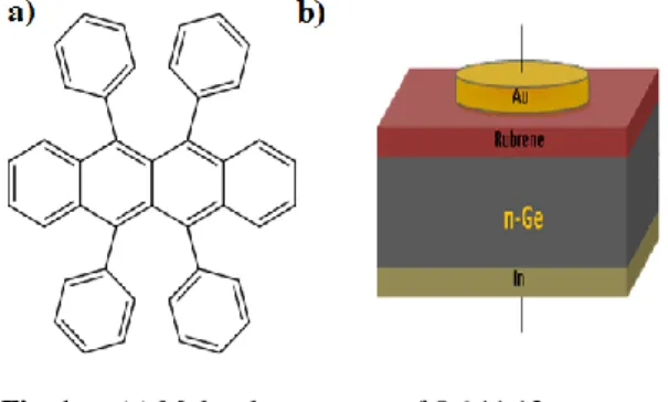
The n-type Ge (100) substrate used in this study has a 500 m thickness and 1-10 cm resistivity. Initially, the substrate has been cleaned in methanol and acetone using ultrasonic agitation for 3 min and rinsed in de-ionized water (18 M). Firstly, The n-Ge substrate is cleaned using the Radio Corporation of America (RCA) cleaning method [15,20]. Ohmic contact with low resistance is made by evaporation of indium (In, 99.99% from Kurt J. Lesker) metal with thickness of 150 nm in 5x10⁻⁶ Torr on the backside of the n-Ge substrate and then by thermal annealing at 400 C for 2 min in vacuum. The rubrene (from Sigma-Aldrich) which its chemical structure is shown in Fig.1(a) was dissolved in toluene with a concentration of 10 mg ml-1. This solution was stirred for 5 min at a magnetic stirrer. The solution was prepared and kept in MBraun glovebox maintaining a N2 environment. A rubrene organic film is prepared on the n-Ge substrate by the spin coating technique at a spinning rate of 1200 rpm for 60 s with a Laurell Spin Coater. This methods of the most common techniques for applying
thin films. The advantage of spin coating is its ability to quickly and easily produce very uniform films from a few nanometers to a few microns in thickness. Schottky contacts are prepared on rubrene organic film with a diameter of 2 mm by a metal shadow mask by evaporating gold (Au, 99.95% from Kurt J. Lesker) metal with thickness of 150 nm in 5x10⁻⁶ Torr. High purity In and Au metal contacts were thermally evaporated from a tungsten filament in a high vacuum coating unit (Edwards, E-306A) to form the bottom and top contact onto rubrene/n-Ge film surface, respectively. The schematic diagram of the prepared device is shown in Fig. 1(b). The I–V measurements were performed by a Keithley 2410 SourceMeter at temperature range from 150 to 300 K using an ARS Closed Cycle Cryostat Model DE202 AI and a Lake Shore model 331 temperature controller.
Fig. 1. (a) Molecular structure of 5,6,11,12-tetraphenylnaphthacene (rubrene) organic compound. (b) Structure of Au/rubrene/n-Ge Schottky device for electrical characterization.
3. RESULTS AND DISCUSSION
3.1. Current–Voltage Characteristics of the Diode Experimentally observed Current–Voltage (I-V) characteristics are mostly semi-logarithmic and they are compatible with thermionic emission theory. The I–V curves can be investigated by the following equations [21-23]: 𝐼 = 𝐼0[𝑒𝑥𝑝 ( 𝑞𝑉 𝑛𝑘𝑇) − 1] ; 𝐼0= 𝐴𝐴 ∗𝑇2𝑒𝑥𝑝 (−𝑞Φ𝐵 𝑘𝑇) (1) where 𝐼0 is saturation current, 𝑛 is the diode quality factor, q is the electronic charge, A is the Schottky diode contact area, A* is the effective Richardson constant and is equal to 143 A cm-2 K-2 for n-type Ge [24,25], T is the absolute temperature in Kelvin. 𝐼0 is the saturation current derived from the straight line intercept of ln I at zero-bias. The Φ𝐵 Schottky barrier height and 𝑛 ideality factor values of Au/rubrene/n-Ge can be determined from intercepts and slopes of the voltage dependent of forward-bias ln I curve respectively, as [21,22,26]: Φ𝐵= 𝑘𝑇 𝑞 𝑙𝑛 ( 𝐴𝐴∗𝑇2 𝐼0 ) and 𝑛 = 𝑞 𝑘𝑇 𝑑𝑉 𝑑𝑙𝑛(𝐼) (2) 𝑛 equals to 1 for an ideal diode. However, 𝑛 has usually a value greater than unity. High values of 𝑛 can be attributed to the presence of the interfacial thin layer, a wide distribution of low-Schottky barrier height patches
(or barrier inhomogeneities) and to the bias voltage dependence of the Schottky barrier height [26].
Fig. 2 displays the I–V characteristics of the Au/rubrene/n-Ge diode in the temperature range of 150– 300 K. The saturation current (I0) values were
determined from the linear portion intercept of lnI–V at V=0 in the temperature range of 150–300 K. These curves indicate a very strong temperature dependence of the Schottky diodes.
Fig. 2. Current-Voltage of characteristics of Au/rubrene/n-Ge Schottky barrier diode.
The values of saturation current (I0) were obtained from
the linear portion intercept of ln I–V at V = 0 in the temperature range of 150–300 K. The values of barrier height (Φ𝐵) were calculated according to this I0 values.
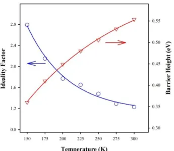
The calculated values of 𝑛 and Φ𝐵 for the Au/rubrene/n-Ge diode range from 2.398 and 0.360 eV (at 150 K) to 1.230 and 0.553 eV (at 300 K), respectively. Φ𝐵 and 𝑛 plots as a function of Au/rubrene/n-Ge diode are presented in Fig. 3. As seen in Fig. 3 the Schottky barrier height (Φ𝐵) decreases and the ideality factor (n) increases with decrease in temperature. Werner and Güttler [27] have suggested that such dependence is created by barrier inhomogeneity which can be caused by various interface properties, which, in turn, depends on different factors such as the metal, the deposition process, the surface treatment, and the surface defects density [27–29]. High 𝑛 values can be attributed to the presence of the interfacial layer and lateral inhomogeneous barrier height distributions [30-36]. On the other hand, the large values of n are also referred to the existence of an organic layer [11,20,26,35,37] plus thin native oxide layer at metal semiconductor interface [38-41] or to the presence the actual conduction process dominating in the junction in literature.
Fig. 3. Temperature dependence of ideality factor and barrier height of Au/rubrene/n-Ge Schottky barrier diode.
In Schottky diodes, the series resistance is one of the most important parameters governing the electrical properties of diodes. In order to determine the value of series resistance, we analyzed the I–V characteristics of the diode using Cheung and Cheung model [42]. According to this method, the forward bias current– voltage characteristics due to the thermionic emission theory of Schottky contacts can be expressed as Eq. 1. If 𝐼0 saturation current is substituted into this expression and then extracting the applied voltage V from the equation , one obtains
𝑉 = 𝐼𝑅𝑠+ 𝑛𝐵+ 𝑛𝑘𝑇
𝑞 𝑙𝑛 ( 𝐼
𝐴𝐴∗𝑇2) (3) By differentiating this equation with respect to I and rearranging we find that
𝑑𝑉 𝑑𝑙𝑛(𝐼)=
𝑛𝑘𝑇
𝑞 + 𝐼𝑅𝑠 (4) 𝑑𝑉/𝑑𝑙𝑛(𝐼) versus I plot should yield straight lines in the downward curvature region of 𝑙𝑛𝐼 − 𝑉 plot in accordance with Eq. 4 and its slope gives the series
resistance (𝑅𝑠) and its intercept on the current axis gives 𝑛𝑘𝑇 𝑞⁄ .
To obtain barrier height (B), Cheung and Cheung defined a function as [15,20,42]
𝐻(𝐼) = 𝑉 − (𝑛𝑘𝑇 𝑞 ) 𝑙𝑛 (
𝐼
𝐴𝐴∗𝑇2) = 𝑛𝐵+ 𝐼𝑅𝑠 (5) In Fig. 4 we give the plots of 𝑑𝑉/𝑑𝑙𝑛(𝐼) and H(I) versus I for Au/rubrene/n-Ge Schottky diodes at room temperature. The values of 𝑅𝑠 and n were calculated from 𝑑𝑉/𝑑𝑙𝑛(𝐼) versus I curve, yielding 𝑅𝑠=7.65 and n=1.25 for Au/rubrene/n-Ge diode at room temperature. Similarly, the plot of H(I) versus I gives the series resistance and the barrier height 𝐵. The values of 𝐵 and 𝑅𝑠 were calculated, yielding values of 𝐵= 0.542 eV and 𝑅𝑠= 7.66 for Au/rubrene/n-Ge diode at room temperature. It should be noted that the value of n obtained from the 𝑑𝑉/𝑑𝑙𝑛(𝐼) versus I curves is higher than that of the forward-bias ln I versus V plot. This can be attributed to the effect of series resistance, interface states and voltage drop across the interfacial layer [38-41].
Fig. 4. dV/d(lnI)-I and H(I)-I characteristics of Au/rubrene/n-Ge Schottky barrier diode at 300 K. Table 1. Temperature dependent values of diode parameters determined by different methods for an Au/Rubrene/n-Ge
Schottky barrier diode.
T(K) I-V 𝑑𝑉/𝑑𝑙𝑛(𝐼) − 𝐼 H(I) - I n 𝐵 n 𝑅𝑠 𝐵 𝑅𝑠 150 2.39 0.360 1.92 8.18 0.386 8.18 175 2.15 0.403 1.66 7.96 0.433 7.96 200 1.77 0.450 1.51 7.82 0.466 7.93 225 1.65 0.479 1.49 7.75 0.484 7.82 250 1.48 0.505 1.46 7.71 0.502 7.72 275 1.29 0.531 1.34 7.69 0.525 7.71 300 1.23 0.553 1.25 7.65 0.542 7.66
The results obtained have been listed in Table 1. in the temperature range of 150–300 K, together with the n and
𝐵 values calculated from the current-voltage
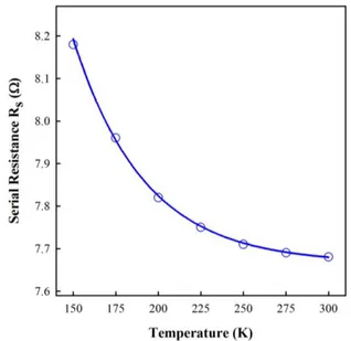
Fig. 5. Variation of 𝑅𝑆 with temperature of Au/Rubrene/n-Ge Schottky barrier diode.
characteristics using Eqs. (4) and (5). As seen from the table, the values obtained by different techniques are in good agreement with each other. The variations of n and
𝐵 with temperature have already been discussed above. On the other hand, the values of series resistance 𝑅𝑠 calculated from the Cheung and Cheung plots decrease by increasing temperature as seen Fig. 5. This decreasing in 𝑅𝑠 can be attributed to the decrease of n with increase of temperature and also to the rising of free carrier concentration at higher temperatures.
Chawanda et al. [43] have studied the electronic properties of the Au/n-Ge (100) Schottky contacts from their current–voltage characteristics at varying temperatures from 150 to 300 K. Khurelbaatar et al. [25] have fabricated the Au/n-Ge Schottky barrier diodes and investigated on their electrical properties using the current–voltage characteristics at room temperature. They have been cross-checked Schottky barrier properties of Au/n-Ge Schottky barrier diodes by various analysis techniques such as forward I–V, C–V, Cheung’s, and Norde’s methods. Chawanda et al. [43] and Khurelbaatar et al. [25] have determined effect of the
temperature on junction parameters n , 𝐵 and 𝑅𝑠. This study results have been compared to theirs results and listed Table 2. for at room temperature values.
3.2. Analysis of Inhomogeneous Barrier Height of the Diode
Chand et al. [46,47] have analyzed Gaussian distribution of barrier heights in inhomogeneous Schottky diodes The current–voltage characteristics of inhomogeneous Schottky diodes have been generated by using analytically solved thermionic-emission diffusion equation incorporating Gaussian distribution of barrier heights and by direct numerical integration over a barrier height range [44]. The Schottky barrier height inhomogeneity of the Au/rubrene/n-Ge Schottky diode was considered by Gaussian distribution of the barrier heights [35, 45-52]. Werner and Güttler [13,27,45] have proposed that the abnormal behavior can be explained by assuming a Gaussian distribution of Schottky barrier height with a mean barrier height Φ̅𝐵0 (mean) and a zero-bias standard deviation 𝜎𝑠0 .
𝑃(Φ𝑎𝑝) = 1
𝜎𝑠0√2𝜋𝑒𝑥𝑝 [−
(Φ𝐵−Φ̅𝐵0)2
2𝜎𝑠02 ] (6) where 1 𝜎⁄ 𝑠0√2𝜋 is the normalization constant of the Gaussian barrier distribution. The Gaussian distribution of the Schottky barrier height yields the following expression for experimental apparent Schottky barrier height at zero bias. Their relation in a simple form, proposed by Chand and Kumar [21,28,44,46,47,53] can be given as,
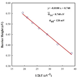
Φ𝑎𝑝= Φ̅𝐵0− 𝑞𝜎𝑠02
2𝑘𝑇 (7) where Φ𝑎𝑝 is the apparent barrier height measured experimentally. Φ̅𝐵0 and 𝜎𝑠0 are the mean Schottky barrier height and its standard deviation at zero-bias (V=0), respectively. The temperature dependence of 𝜎𝑠0 is usually small and can be neglected. The plot of Φ𝑎𝑝 versus 1/2kT (as show in Fig. 6) should be a straight line that gives Φ̅𝐵0 and 𝜎𝑠0 from the intercept and slope, respectively. The mean value Φ̅𝐵0 is 0.740 eV and standard deviation 𝜎𝑠0 equals to 120 mV, respectively. A low value of for homogeneous Schottky type contacts is expected. However, 120 mV value is not low and it confirms the presence of inhomogeneous barrier height for Au/rubrene/n-Ge device [13,27,46,54,55].
Table 2. Comparison of diode parameters determined for an Au/n-Ge and an Au/Rubrene/n-Ge Schottky barrier diodes.
I-V 𝑑𝑉/𝑑𝑙𝑛(𝐼) − 𝐼 H(I) - I
n 𝐵 n 𝑅𝑠 𝐵 𝑅𝑠 Ref.
Au/rubrene/n-Ge 1.23 0.553 1.25 7.65 0.542 7.66 This work
Au/n-Ge 1.34 0.590 1.48 7.01 0.470 7.14 [ 25]
Au/n-Ge 1.12 0.428 -- -- -- -- [42]
Au/n-Ge 1.10 0.610 -- -- -- -- [18]
Fig. 6. Barrier height vs. 1/(2kT) curves for Au/rubrene/n-Ge Schottky barrier diode.
The observed variation of ideality factor with temperature in the model is given by [21,28,44,53]
1
𝑛𝑎𝑝− 1 = −𝜌2+ 𝑞𝜌3
2𝑘𝑇 (8)
where 𝑛𝑎𝑝 is the apparent ideality factor (experimental data) and the coefficients 𝜌2 and 𝜌3 quantify the voltage deformation of the barrier height distribution. The plot of n versus 1/2kT (as show in Fig. 7) should be straight line that gives voltage coefficients 𝜌2 and 𝜌3 from the intercept and slope respectively. The values of 𝜌2 and 𝜌3 were obtained 0.184 and 0.020 in 150– 300 K temperature ranges.
Fig. 7. Temperature dependence of ideality factor (1/n-1) for Au/n-Ge Schottky barrier diode
The 𝐵 is also determined by means of the conventional Richardson plot of the saturation current I0. In this case,
Eq. (2) can be obtained as [20,26,31-40]
𝑙𝑛 (𝐼0
𝑇2) = 𝑙𝑛(𝐴𝐴
∗) −𝑞̅𝐵0
𝑘𝑇 (9) The conventional activation energy experimental 𝑙𝑛(𝐼0⁄𝑇2) vs. 1 𝑘𝑇⁄ plot (as show in Fig. 8) has showed nonlinearity behavior at low temperatures, as indicated above. 𝑙𝑛(𝐼0⁄𝑇2) versus 1 𝑘𝑇⁄ should be a straight line that gives Φ̅𝐵0 and A* from the intercept and slope, respectively. The values of Φ̅𝐵0 and A* are 0.512 eV and 35 A cm-2 K-2 in 150–200 K temperature range and as 0.188 eV and 38 A cm-2 K-2 in 250–300 K temperature range. The A* values are much lower than the theoretical value of 143 A cm-2 K-2 for n-Ge [24]. This deviation in Richardson plots may be due to the inhomogeneous barrier and potential fluctuations at the metal-semiconductor interface; that is, the current through the contact will flow preferably through the lower barriers [31,43,54].
Fig. 8. 𝑙𝑛(𝐼0⁄𝑇2) versus 1/kT plots for the Au/rubrene/n-Ge
Schottky barrier diode according to two Gaussian distributions.
Since the conventional Richardson plot deviates from linearity at low temperatures due the barrier inhomogeneity, it can be modified by combining Eq. (1) and (7), to explain these discrepancies, according to the Gaussian distribution of the barrier height [26,35,43,56] we gets ln (𝐼0 𝑇2) − ( 𝑞2𝜎𝑠2 2𝑘2𝑇2) − 𝑙𝑛(𝐴𝐴 ∗) −𝑞Φ̅𝐵0 𝑘𝑇 (10) Using the experimental 𝐼0 data, a modified 𝑙𝑛(𝐼0⁄𝑇2) − (𝑞2𝜎
𝑠2⁄2𝑘2𝑇2) versus 1/kT plot according to Eq. (10) should give a straight line with the slope directly yielding the mean barrier height and the intercept (= ln AA*) at the ordinate determining A* for a given diode area A. The 𝑙𝑛(𝐼0⁄𝑇2) − (𝑞2𝜎𝑠2⁄2𝑘2𝑇2) using two values of A* and Φ̅𝐵0 obtained for temperature ranges of 150–300 K. The modified 𝑙𝑛(𝐼0⁄𝑇2) − (𝑞2𝜎𝑠2⁄2𝑘2𝑇2) versus 1/kT plots for the values of Φ̅𝐵0 and A* are 0.816 eV and 121 A/cm2K2 have been given in Fig. 8. Richardson constant
value of A* is very close to the theoretical value 143 A cm-2 K-2 [32]. 1/2kT plot at higher temperatures in Fig. 8. This value is smaller than the reported of 143 A cm-2 K-2. This may be due to greater inhomogeneities at the interface.
Fig. 9. Modified Richardson 𝑙𝑛(𝐼0⁄𝑇2) − (𝑞2𝜎𝑠2⁄2𝑘2𝑇2) versus 1/kT plots for the Au/rubrene/n-Ge Schottky barrier diode according to Gaussian distributions.
4. CONCLUSIONS
The spin coated grown monolayer rubrene was employed as the interlayer in Au/n-Ge Schottky barrier diodes. We investigated rubrene interlayer effects on Schottky barrier parameters such as ideality factor, barrier height, and series resistance of Au/n-Ge Schottky barrier diode. It is observed that, the electrical parameters strongly depend on the organic layer between the metal– semiconductor contacts. Increase in the temperature causes an exponential decrease in the ideality factor. It is clearly seen that the values decrease more rapidly at low temperatures. However, temperature has a lower effect on the determination of ideality factor values at high temperatures. It can be also estimated that the values become closer to its ideal value at very high temperatures. In contrast to ideality factor, it is observed that the potential barrier height values increase with the temperature and the variation of potential barrier height with temperature is linear and sensitively temperature dependent. Effect of temperature on the serial resistance values have been illustrated in the Fig. 5. To check accuracy of the results, Cheung–Cheung method is also employed to calculate the electrical properties. It can be said that the values are good agreement with those obtained from I–V method. In order to obtain evidence of a Gaussian distribution of barrier heights, we have plotted 𝐵 vs. 1/2kT graphs, and from which the of value Φ̅𝐵0=0.740 eV and 𝜎𝑠0= 120 mV for barrier heights with a mean barrier height and standard deviation respectively, have been obtained. Our results show that organic interlayer is a particularly important factor that
influences the electronic properties of a diode system, depending on the temperature and the n-Ge wafer. We found that the rubrene interlayer could improve Au/n-Ge Schottky barrier diode properties to enable high quality Ge and rubrene devices with Schottky contacts in the future.
ACKNOWLEDGEMENT
This work is supported by Selçuk University BAP office with the Research Project number 15401014. The author acknowledge Assoc. Prof. Dr. Ö.F. YÜKSEL for fruitful discussion and valuable contribution in experiment measurement.
REFERENCES
[1] Virkar, A. A., Mannsfeld, S., Bao, Z. and Stingelin, N. “Organic Semiconductor Growth and Morphology Considerations for Organic Thin‐Film Transistors”, Advanced Materials, 22: 3857-3875, (2010).
[2] Schmechel, R. and von Seggern, H. “Electronic traps in organic transport layers”, Physica Status Solidi (a), 201: 1215-1235, (2004).
[3] Mishra, A. and Bäuerle, P. “Small Molecule Organic Semiconductors on the Move: Promises for Future Solar Energy Technology”, Angewandte Chemie International Edition, 51: 2020-2067, (2012).
[4] Djurovich, P. I., Mayo, E. I., Forrest, S. R. and Thompson M. E. “Measurement of the lowest unoccupied molecular orbital energies of molecular organic semiconductors”, Organic Electronics, 10: 515-520, (2009).
[5] Wohlgenannt, M. “Organic magnetoresistance and spin diffusion in organic semiconductor thin film devices”, Physica Status Solidi RRL, 6: 229-242, (2012). [6] Huang, L.S. and Chen, C.H. “Recent progress on
molecular organic electroluminescent materials and devices”, Materials Science and Engineering: R: Reports, 39: 143-222, (2002).
[7] Chan, M.Y., Lai, S.L., Fung, M.K., Lee, C.S. and Lee, S.T. “Doping-induced efficiency enhancement in organic photovoltaic devices”, Applied Physics Letters, 90: 023504, (2007).
[8] Karak, S., Lim, J. A., Ferdous, S., Duzhko, V. V. and Briseno, A. L. “Photovoltaic Effect at the Schottky Interface with Organic Single Crystal Rubrene”, Advanced Functional Materials, 24: 1039-1046, (2014). [9] Chen, Y. and Shih, I. “High mobility organic thin film transistors based on monocrystalline rubrene films grown by low pressure hot wall deposition”, Applied Physics Letters, 94: 083304, (2009).
[10] Horowitz, G. “Organic Field-Effect Transistors”, Advanced Materials, 10: 365-377, (1998).
[11] Dökme, İ. and Altındal, Ş. “On the intersecting behavior of experimental forward bias current-voltage (I-V) characteristics of Al/SiO2/p-Si (MIS) Schottky diodes at low temperatures”, Semiconductor Science and Technology, 21: 1053-1058, (2006).
[12] Karataş, Ş., Altındal, Ş. and Çakar, M. Physica B, 357: 386-397, (2005).
[13] Werner, J.H. and Guttler, H.H. “Temperature dependence of Schottky barrier heights on silicon”, Journal of Applied Physics, 73: 1315-1319, (1993).
[14] Cimili, F.E., Sağlam, M., Efeoğlu, H. and Türüt, A. “Temperature-dependentcurrent–voltage characteristics of the Au/n-InP diodes with inhomogeneous Schottky barrier height”, Physica B, 404: 1558-1562, (2009). [15] Yüksel, Ö. F. “Temperature dependence of current–
voltage characteristics of Al/p-Si (100) Schottky barrier diodes”, Physica B, 404: 1993-1997, (2009).
[16] Wu, J. R., Wu, Y.H., Hou, C.Y., Wu, M.L., Lin, C.C. and Chen, L.L. “Impact of fluorine treatment on Fermi level depinning for metal/germanium Schottky junctions”, Applied Physics Letters, 99: 253504, (2011).
[17] Janardhanam, V., Yun, H.J., Lee, J., Reddy, V. R., Hong, H., Ahn, K.S. and Choi, C.J. “Depinning of the Fermi level at the Ge Schottky interface through Se treatment”, Scripta Materialia, 69: 809-811, (2013).
[18] Khurelbaatar, Z., Kang, M., Shim, K., Yun, H., Lee, J., Hong, H., Chang, S., Lee, S. and Choi C. “Temperature dependent current–voltage characteristics of Au/n-type Ge Schottky barrier diodes with graphene interlayer”, Journal of Alloys and Compounds, 650: 658-663, (2015).
[19] Lieten, R. R., Degroote, S., Kuijk, M. and Borghs G. “Ohmic contact formation on n-type Ge”, Applied Physics Letters, 92: 022106, (2008).
[20] Şimşir, N., Şafak, H., Yüksel, Ö.F. and Kuş, M. “Investigation of current–voltage and capacitance– voltage characteristics of Ag/perylene-monoimide/n-GaAs Schottky diode”, Current Applied Physics, 12: 1510-1514, (2012).
[21] Chand S. and Kumar, J. “Current-voltage characteristics and barrier parameters of Pd2Si/p-Si(111) Schottky diodes in a wide temperature range”, Semiconductor Science and Technology, 10: 1680-1688, (1995). [22] Rhoderick, E. H. “Metal-Semiconductor Contacts”,
Clarendon, Oxford, UK, (1978).
[23] Sze, S.M. “Physics of Semiconductor Devices”, John Wiley and Sons, New York, USA, (1981).
[24] Zhiqiang, L., Xia, A., Quanxin, Y., Meng, L., Xing, Z. and Ru, H. “Tuning Schottky Barrier Height in Metal/n-Type Germanium by Inserting an Ultrathin Yttrium Oxide Film”, ECS Solid State Letters, 1: Q33-Q34, (2012).
[25] Khurelbaatar, Z., Kil, Y., Yun, H., Shim, K., Kim, K., Lee, S., Choi, C. and Nam, J. T. “Modification of Schottky barrier properties of Au/n-type Ge Schottky barrier diode using monolayer graphene interlayer”, Journal of Alloys and Compounds, 614: 323-329, (2014).
[26] Güzeldir B., Sağlam, M., Ateş, A. and Türüt, A. “Determination of the some electronic parameters of nanostructure copper selenide and Cu/Cu3Se2/n-GaAs/In structure”, Journal of Alloys and Compounds, 627: 200-205, (2015)
[27] Werner, J.H. and Güttler, H.H. “Barrier inhomogeneities at Schottky contacts”, Journal of Applied Physics, 69: 1522-1533, (1991).
[28] Kumar, A., Vinayak, S. and Singh, R. “Micro-structural and temperature dependent electrical characterization of
Ni/GaN Schottky barrier diodes”, Current Applied Physics, 13: 1137-1142, (2013).
[29] Kalinina, E.V., Kuznetsov, N.I., Dmitriev, V.A., Irvine, K.G. and Carter, C.H. J. “Schottky barriers on n-GaN grown on sic”, Journal of Electronic Materials, 25: 831-834, (1996).
[30] Vural, Ö., Şafak, Y., Altındal, Ş. and Türüt, A. “Current– voltage characteristics of Al/Rhodamine-101/n-GaAs structures in the wide temperature range”, Current Applied Physics, 10: 761-765, (2010).
[31] Yüksel, Ö.F., Tuğluoğlu, N., Şafak, H., Nalçacıgil, Z. and Karadeniz, S. “Analysis of temperature dependent electrical properties of Au/perylene-diimide/n-Si Schottky diodes”, Thin Solid Films, 534: 614-620, (2013).
[32] Bengi, A., Altındal, Ş., Özçelik, S., Agaliyeva, S.T. and Mammadov, T.S. “Analysis of temperature dependent electrical characteristics of Au/n-GaAs/GaAs structures in a wide temperature range”, Vacuum, 83: 276-281, (2009).
[33] Altuntaş, H., Altındal, Ş., Özçelik, S. and Shtrikman, H. “Electrical characteristics of Au/n-GaAs Schottky barrier diodes with and without SiO2 insulator layer at room temperature”, Vacuum, 83: 1060-1065, (2009).
[34] Yüksel, Ö.F., Kuş, M., Şimşir, N., Şafak, H., Şahin, M. and Yenel, E. “A detailed analysis of current-voltage characteristics of Au/perylene-monoimide/n-Si Schottky barrier diodes over a wide temperature range”, Journal of Applied Physics, 110: 024507, (2011).
[35] Barış, B., Yüksel, Ö.F., Tuğluoğlu, N. and Karadeniz, S. “Double barrier heights in 5, 6, 11, 12-tetraphenylnaphthacene (rubrene) based organic Schottky diode”, Synthetic Metals, 180: 38-42, (2013).
[36] Güllü, Ö., Aydoğan, Ş. and Türüt, A. “Electronic parameters of high barrier Au/Rhodamine-101/n-InP Schottky diode with organic ınterlayer”, Thin Solid Films, 520: 1944-1948, (2012).
[37] Soylu, M., Abay, B. and Onganer, Y. “Electrical characteristics of Au/Pyronine-B/moderately doped n-type InP Schottky structures in a wide temperature range” Journal of Alloys and Compounds, 509: 5105-5111, (2011).
[38] Tuğluoğlu, N., Karadeniz, S. and Altındal, Ş. “Effect of series resistance on the performance of silicon Schottky diode in the presence of tin oxide layer”, Applied Surface Science, 239: 481-489, (2005).
[39] Şahin, M., Şafak, H., Tuğluoğlu, N. and Karadeniz, S. “Temperature-dependent of current-voltage characteristics of Ag/p-SnS Schottky barrier diodes”, Applied Surface Science, 242: 412-418, (2005). [40] Karadeniz, S., Tuğluoğlu, N., Şahin, M. and Şafak, H.
“Series resistance calculation for Ag contacts on single crystal layered p-SnS and p-SnSe compound semiconductors in the wide temperature range”, Microelectronic Engineering, 81: 125-131, (2005). [41] Tuğluoğlu, N., Yakuphanoğlu, F. and Karadeniz, S.
“Determination of the interface state density of the In/p-Si Schottky diode by conductance and capacitance– frequency characteristics”, Physica B: Condensed Matter, 393: 56-60, (2007).
[42] Cheung, S.K. and Cheung, N.W. “Extraction of Schottky diode parameters from forward current‐voltage
characteristics”, Applied Physics Letters, 49: 85–87, (1986).
[43] Chawanda, A., Mtangi, W., Auret, F. D., Nel, J., Nyamhere, C. and Diale M. “Current–voltage temperature characteristics of Au/n-Ge (1 0 0) Schottky diodes”, Physica B: Condensed Matter, 407: 1574-1577, (2012).
[44] Murakami, H., Fujioka, T., Ohta, A., Bando, T., Higashi, S. and Miyazaki S. “Characterization of interfaces between chemically cleaned or thermally oxidized germanium and metals”, ECS Transactions, 33: 253-262, (2010).
[45] Güttler, H.H. and Werner, J.H. “Influence of barrier inhomogeneities on noise at Schottky contacts”, Applied Physics Letters, 56: 1113-1115, (1990).
[46] Chand, S. and Kumar, J. “On the existence of a distribution of barrier heights in Pd2Si/Si Schottky diodes”, Journal of Applied Physics, 80: 288-294, (1996).
[47] Chand, S. and Kumar J., “Current transport in Pd2 Si/n-Si(100) Schottky barrier diodes at low temperatures”, Applied Physics A, 63: 171-178, (1996).
[48] Gümüş, A., Türüt, A. and Yalçın, N. “Temperature dependent barrier characteristics of CrNiCo alloy Schottky contacts on n-type molecular-beam epitaxy GaAs”, Journal of Applied Physics, 91: 245-250, (2002). [49] Yıldırım, N., Ejderha, K., and Türüt, A. “On
temperature-dependent experimental I - V and C - V data of Ni / n -GaN Schottky contacts”, Journal of Applied Physics, 108: 114506, (2010).
[50] Schmitsdorf, R.F., Kampen, T.U. and Mönch, W. “Correlation between barrier height and interface structure of AgSi (111) Schottky diodes”, Surface Science, 324: 249-256, (1995).
[51] Mönch, W. “Barrier heights of real Schottky contacts explained by metal-induced gap states and lateral inhomogeneities”, Journal of Vacuum Science & Technology B, 17: 1867-1876, (1999).
[52] Farag, A.A.M. and Yahia, I.S. “Rectification and barrier height inhomogeneous in Rhodamine B based organic Schottky diode”, Synthetic Metals, 161: 32-39, (2011). [53] Chand, S. and Kumar, J. “Effects of barrier height
distribution on the behavior of a Schottky diode”, Journal of Applied Physics, 82: 5005-5010, (1997). [54] Yüksel, Ö.F., Tuğluoğlu, N., Gülveren, B., Şafak, H. and
Kuş, M. “Electrical properties of Au/perylene-monoimide/p-Si Schottky diode”, Journal of Alloys and Compounds, 577: 30-36, (2013).
[55] Song, Y.P., Van Meirhaeghe, R.L., Laflere, W.F. and Cardon, F. “On the difference in apparent barrier height as obtained from capacitance-voltage and current-voltage-temperature measurements on Al/p-InP Schottky barriers”, Solid State Electronics, 29: 633-638, (1986). [56] Çaldıran, Z., Aydoğan, Ş., Yeşildağ, A., Ekinci, D.,
Kurudirek, S.V. and Türüt A. “Temperature-dependent current–voltage measurements of Au/C9H7N/p-Si: Characterization of a metal–organic-semiconductor device”, Materials Science in Semiconductor Processing, 34: 58-64, (2015).