Broadband One Way Propagation via Dielectric
Waveguides with Unequal Effective Index
B. B. Öner
1*, K. Üstün
2, 3, H. Kurt
1, A. K. Okyay
4, G. Turhan-Sayan
2 1 Nanophotonics Research Laboratory, Department of Electrical and Electronics Engineering, TOBB University ofEconomics and Technology, 06560 Ankara, Turkey
2 Department of Electrical and Electronics Engineering, Middle East Technical University, 06800 Ankara, Turkey 3 Department of Electrical and Electronics Engineering, Hitit University, 19030 Çorum, Turkey 4 Department of Electrical and Electronics Engineering, UNAM-National Nanotechnology Research Center, Institute
of Materials Science and Nanotechnology, Bilkent University, 06800 Ankara, Turkey *[email protected]
Abstract
—
We present an efficient approach for broad band one way propagation of light by parallel and unequal dielectric waveguides leading different effective phase shifts. Three dimensional numerical simulations show that 30% operating bandwidth is achieved.Keywords: Guided waves, Mode conversion, Integrated
Optics Devices.
To date, passive/linear optical component designs have shown a great promise providing novel devices operating within broadband frequency regions. The improvement of optical designs gave rise to requirement of different light manipulation processes. Mode conversion is an important desideratum, as the light wave should conform to the modal distribution of the cascaded optical devices. Additionally, mode order conversion is a versatile tool for one way propagation devices. Due to the reciprocity theorem, linear systems lack ability to operate as optical diodes. A mode conversion process (transforming fundamental mode to first order mode) between single and multimode waveguides inhibits propagation through a particular way while providing high transmission efficiency through the opposite one if the input waves comply with intended modal distributions.
Several techniques are proposed to obtain mode order conversion [1-4]. In the literature, the mainly encountered problem of compact mode conversion process is the restriction of operating frequency range. If the optical component is desired to be broad band, devices with excessive lengths are required, namely, a trade-off exists between operating frequency regime and the size of the converter.
In the present study, a mode order converter showing one way propagation property is proposed. As the structure is composed of simple wave guide structures, the fabrication of the device requires easier manufacturing steps than the approaches utilizing mainly photonic crystals that are periodic dielectric medium.
The mode converter consists of two parallel dielectric waveguides with unequal structural parameters. Inequality of these waveguides generates different effective wave vectors (k) for the same frequency interval. Two dielectric waveguides that differ in width (w) are utilized in this study to introduce a phase difference of ΔΦ=π between two equal beams.
Dispersion diagrams of rectangular waveguides with different w values are investigated by the help of numerical frequency domain simulations [5]. The phase shifts exposed to the beams propagating throughout these waveguides are expressed as ΔΦ=LΔk, where L represents the length of the waveguides through the propagation direction. The proper arrangement of L provides π phase shift, Φ1-Φ2
= π, between the outputs of differential waveguides
w1 and w2. For a determined frequency, a conversion
length (Lc) can be calculated for π (180
0
) phase shift with the known Δk value Lc=π/Δk.
Perfect π phase shift is achievable for particular frequencies regarding the corresponding k values. In other words, it is not possible to obtain constant wave vector difference regarding dielectric waveguides
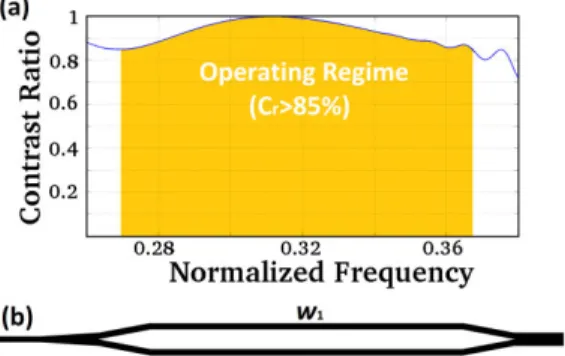
Fig. 1. (a) Contrast ratio is shown. The operating frequency regime where contrast ratio is over 85% is highlighted. (b) The geometry of the mode order converter. w1 and w2 represents the width values of the corresponding waveguides.
556
WH4.3 (Contributed)
4:00 PM - 4:15 PM
with definite width difference Δw=w1-w2.
Nevertheless, dispersion diagrams indicate that the propagation vectors slightly vary within a spectral region. In order to transfer the operating narrow frequency regime to a broad one, we regarded 5o
phase shift error as negligible and calculated upper and lower frequency limits with respect to this assumption. In addition, the center frequency is determined based on a 5o phase shift error with the
corresponding peak value of the w-k relation. In this manner, the upper and lower limits of the frequency interval are extended.
Regarding the maximized bandwidth, the width difference Δw is chosen as 0.02a with the lengths of the waveguides w1=0.77a and w2=0.75a. The
thicknesses of both of the waveguides are fixed at
t1=t2=0.70a, where a is the scaling length constant.
Consequently, the optimized Δk and conversion length values are found as Δk=2π×0.014a1 and Lc=35.77a, respectively.
In order to verify the estimated bandwidth in frequency domain results and to obtain transmission efficiency of the structure, time domain simulations are utilized [6]. The forward and backward transmission efficiencies (f and b, respectively) are computed and the main figure of merit of the current study contrast ratio, cr 2(fb) (fb) between
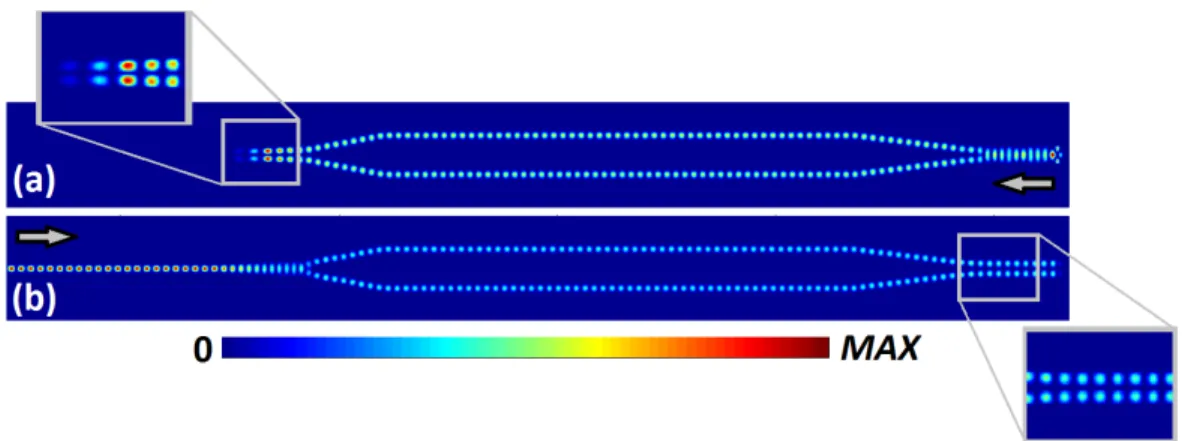
these values is given in Fig. 1(a). Operating bandwidth of the device is 30% regarding the criteria of achieving contrast ratio over 85%. The upper and lower boundaries are a/λ=0.2697 and a/λ=0.3671, respectively. The transmission efficiency of forward propagation is over 84% in this regime. Overall design used in the simulations is shown in Fig. 1(b). Electric field intensity distributions of the forward and backward propagating waves with the frequency value a/λ=0.3117 is given in Fig. 2.
If the center wavelength is chosen to be at 1550 nm, then the waveguide widths are approximately
w1=372 nm and w2=362 nm, where the thickness is
approximately t=338 nm. The length of the device
becomes 25.34 µm. The operating wavelength interval encompasses the whole communication band. In addition, it is possible to fabricate the simple geometry with the given aspects by the help of the current fabrication technology.
In conclusion, three dimensional numerical analyses demonstrate that high contrast ratio one way propagation is achieved with large operating frequency regime using differential dielectric waveguides. This study may lead to enhanced bandwidth optical isolators and related applications of mode order converters by the incorporation of nonlinear optical elements.
ACKNOWLEDGEMENT
HK acknowledges partial support from the Turkish Academy of Sciences.
REFERENCES
[1] B. B. Oner, M. Turduev, I. H. Giden, and H. Kurt, “Efficient mode converter design using asymmetric graded index photonic structures,” Opt. Lett., vol. 38, pp. 220-222, 2013.
[2] V. Liu, D. A. B. Miller, and S. Fan, “Ultra-compact photonic crystal waveguide spatial mode converter and its connection to the optical diode effect,” Opt. Express, vol. 20, pp. 28388-28397, 2012.
[3] M. Turduev, B. B. Oner, I. H. Giden, and H. Kurt, "Mode transformation using graded photonic crystals with axial asymmetry," J. Opt. Soc. Am. B, vol. 30, pp. 1569-1579, 2013.
[4] J. M. Castro, D. F. Geraghty, S. Honkanen, C. M. Greiner, D. Iazikov, and T. W. Mossberg, “Demonstration of mode conversion using anti-symmetric waveguide Bragg gratings,” Opt. Express, vol. 13, pp. 4180-4184, 2005.
[5] S. Johnson and J. Joannopoulos. “Block-iterative frequency-domain methods for Maxwell's equations in a planewave basis,” Opt. Express, vol. 8, pp. 173-190, 2001.
[6] F. Oskooi, D. Roundy, M. Ibanescu, P. Bermel, J. D. Joannopoulos, and S. G. Johnson, “MEEP: a flexible free-software package for electromagnetic simulations by the FDTD method,” Comput. Phys. Commun., vol. 181, pp. 687–702, 2010.
Fig. 2. The steady state intensity distributions at the normalized frequency a/λ=0.3117 is given for (a) backward and (b) forward propagation. Zoom in part of the guided and unguided intensity distributions are shown. Each figure is individually normalized.