E L S E V I E R Synthetic Metals 87 (1997) 219-223
Im T ILS
Electronic properties of polypyrrole/polyindene composite/metal
junctions
A. Bozkurt a, C. Ercelebi b, L. Toppare o,.
'~ Department of Chemistry, Middle East Technical University, 06531 Ankara, Turkey b Department of Physics, Middle East Technical University, 06531 Ankara, Turkey
° Department of Chemistry, Bilkent University, 06533 Ankara, Turkey
Received 16 April I996; accepted 23 December 1996
Abstract
Junction properties between conducting polymer composites of polypyrrole/polyindene (PPy/Pin) with different conductivities and metals like Pt, Au, A1 and In have been investigated. Rectifying junctions were observed for low work function metals, In and A1; however, high work function metals, Pt and Au, were observed to form ohmic contacts to PPy/PIn composite in the sandwich geometry. The rectifying behavior of the metal/composite/Pt junctions improved when the conductivity of the composite was decreased from 1 to 0.01 S/cm. Using the ideal Schottky theory various junction parameters have been determined. All planar junctions were ohmic regardless of the conductivities of the samples.
Keywords: Electronic properties; Polypyrrole; Polyindene; Composite/metal junctions
1. Introduction
The attractiveness of conducting polymers, especially those produced from heterocyclic monomers, have created enormous interest in the past few decades due to their stability and low cost. However, they have poor mechanical properties and processibitity. Due to this reason, considerable progress has begun in improving their mechanical properties. These improvements have been achieved by a method of blending with conventional polymers [ 1-9].
Electrically conductive polymers such as polyacetylene, polypyrrole and polythiophene have found promising appli- cations in electronic devices since the 1960s. In particular, polypyrrole and polypyrrole/poly(N-methylpyrrole) are being studied as active materials in electronic devices and it was reported that these materials form Schottky contacts with A1 and In [ 10-13].
In this present work, a new method for the preparation of polypyrrole/polyindene ( P P y / P I n ) composite/metal junc- tions is suggested and the rectifying effects of metals/com- posite Schottky barrier diodes are discussed using current- voltage (I-V) and capacitance-voltage (C-V) characteris- tics. The synthesis and characterization of the composites with different methods were given in a previous work [ 14].
* Corresponding author.
0379-6779/97/$17.00 © 1997 Elsevier Science S.A. All rights reserved
P I I S 0 3 7 9 - 6 7 7 9 ( 9 7 ) 0 3 8 1 0 . 1
2. Experimental
Composite films of PPy/PIn were electrochemically pre- pared by using two different sets of experiments. In the first, 0.1 M indene monomer in acetonitrile was used for the elec- trochemical polymerization ofindene on a platinum electrode at 2.0 V versus Ag°/Ag + at room temperature. Then electro- chemical polymerization of pyrrole onto a polyindene-coated electrode at a constant potential of 1.0 V versus Ag°/Ag + in a different cell was carried out where the pyrrole concentra- tion was 0.05 M.
In the second set the composite films were prepared by the electrooxidation of indene at a constant potential of 2.0 V versus A g / A g + (10 .2 M) in a cell containing 0.05 M indene. The electrode here was PPy which was previously prepared at a constant potential of 1.0 V versus Ag°/Ag + ( 10-2 M) on a platinum electrode in a different cell contain- ing 0.05 M pyrrole monomer.
Electrochemical polymerizations were carried out in a three-compartment cell equipped with platinum foils ( 1 cm a) as the working and auxiliary electrodes. The solvent-electro- lyte was acetonitrile-tetrabutylammonium tetrafluoroborate
(TBAFB).
For both systems, films with different surface conductivi- ties were produced by varying the electrolyte concentration
220 A. Bozkurt et aL / Synthetic Metals 87 (1997) 219-223
Platinum
I I
Metal PPy/Pin
Fig. 1. Configuration of Pt/composite/metal junctions: top view and cross section.
from 0.1 to 0.01 M. Electrical conductivities of samples were measured via the standard four-probe technique.
The evaporation of metals for the contact formation was done on composite (PPy/Pin) -coated Pt electrodes by using the Nanotech (thin film) evaporator system. A point mask was used during vacuum deposition of different metals. Au, A1 and In were evaporated on the surfaces of the composite films which were synthesized by using both systems. The device structure is illustrated in Fig. 1.
The composite films were about 10 txm thick and the con- tact area was 0.03 cm a. In order to measure forward and reverse I - V characteristics of the devices, current was passed between the two contacts by using a Keithley model 225 constant-current source. The voltage drop across the device was measured by using a Keithley model 614 digital elec- trometer. I - V measurements were carried out at room tem- perature in a dark box.
The room-temperature C - V measurements were made using a 1 MHz capacitance meter of the model DLS-82 semi- trap DLTS (deep level transient spectroscopy) system.
3. Results a n d discussion
For both the first and the second sets of experiments the electrochemically produced composites (PPy/PIn) yielded homogeneous films, at least in terms of conductivity. It was demonstrated that for both systems the conductivities of the films were not greatly affected by the percolation composi- tion, after 80% PPy content [ 14]. The aim of the insulating matrix in the composite was to solve the pinhole problem almost completely and obtain good surface morphology with- out changing the properties of conducting PPy.
The bulk conductivity of the films has major importance when producing a Schottky contact. This property was con- trolled by the low charge density which is associated with the low doping of polymer [ 13]. The production of the films with conductivities ranging from 1 to 0.01 S / c m was carried out by varying the concentration of dopant (TBAFB). We also showed that, as the conductivities of the films lowered, better rectifying characteristics were observed.
Before deposition of the metals as a top electrode, the samples were heat treated (curing, 90 °C) under vacuum in order to prepare the surface for the production of reliable and stable contacts and to remove water, if any, from the com- posite films.
T h e I - V characteristics of p-type PPy in the PPy/Pin com-
posite films were expected to show ohmic behaviors between high work function metals such as Pt ( qSp, = 5.65 eV) and Au
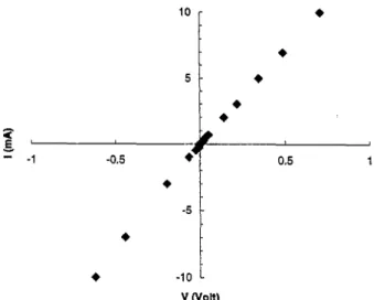
(~bA~ = 5.1 eV). Fig. 2 shows the typical I - V characteristic of the A u - P P y / P I n - P t sandwich structure. Current varies linearly with the applied voltage and the slope of l o g / - l o g V variation is almost unity, which indicates the ohmic behavior of the contacts. This ohmic nature of the contacts was checked by reversing the polarity of the applied voltage and the I - V
characteristics were observed to remain essentially the same with the reversal of applied bias. The forward voltage bias corresponds to a negative voltage at metals (front contact) with respect to Pt back contact. The junction properties of Au-PPy / PIn-Pt structure were observed to be ohmic for both systems regardless of their conductivities.
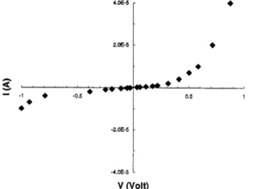
The interface between the PPy/PIn composite and low work function metals such as In (~bln=4.12 eV) and AI (qSA1 =4.28 eV) was expected to make rectifying contact. A1 / In / composite/Ptjunctions have been investigated for dif- ferent film conductivities such as 1, 0.1 and 0.01 S/cm. The
I - V characteristics of these junctions were observed to be
nonohmic and asymmetrical leading to a rectifying behavior. The results showed that the junctions formed from the com- posite films synthesized by the second system with conduc- tivities 1-0.1 S / c m are more rectifying than those obtained by the first system. The better rectifying behavior observed for the metal/composite junctions constructed via the second method even though the films are highly conducting (1-0.1 S/cm) is attributed to the dense Pin insulating phase on the solution side of the composite films which was elucidated by the scanning electron microscopy (SEM) photographs [ 14]. Figs. 3 and 4 illustrate the typical I - V characteristics of In/ composite/Pt junctions prepared by the first and second sys- tems (o- = t S / c m ) , respectively.
The composite films which have conductivities about 0.1 S / c m lead to better rectifying behavior as demonstrated in Fig. 5 (a) and (b) for In/composite and A1/compositejunc- tions, respectively, prepared by the second system. Metal/ conducting-polymer junctions have been investigated previously and it was reported that, for the films with high
10 • - -1 -0.5 4, 5 -5 -10 v (volt) 4. 4~ 0.5 1
Fig. 2. I-V characteristic of Pt/composite/Au sandwich junction (o'= 0.8 S/cm).
A. Bozkurt et al. / Synthetic Metals 87 (1997) 219-223 221 A < , i . 2 7.0E-4 g • -I • 5.0'E-4 3.0E-4 1,0E..4 - % 0 E 4 - 3 . 0 E 4 -5.0E4 -7.0E-4 v (yon) ' i 2
Fig. 3. I - V characteristic of ln/composite/Pt junction (first system, o'= 1 S/cm). - - .o.e .0.4 •
(a)
2.0E-5 1.0E-5 0,2 -1,0E.5 .2.0E-5 V (volt) 9 , 0 ~ 5 , I I 0.4 0,6 4.o~-5 • A < , v w - 1 2.0E-5 - 0 . 5 - 2 . 0 ~ - 5 T , J , , r 0.5 1 -4.0E-5 v (Volt)Fig. 4. I - V characteristic of In/composite/Pt sandwich junction (second system, o-= 1 S / c m ) .
conductivity (10--100 S / c m ) , no evidence for rectifying behavior has been found even with the low work function metals like In and A1 [13].
It is known that the conductivity of the material is important for the construction of a Schottky barrier. High conductivity leads to a narrow depletion width which causes the tunneling currents through the barrier and a bad rectification [ 10]. Thus, the composite films with lower conductivities (0.01 S/ cm) were prepared. The I - V behavior of junctions formed with such films gave even better rectifying behaviors. In this case it was clearly observed that the conductivities of the samples are dominant over the insulating layer of the films produced by the second system. This means that there are almost no changes in the rectifying behavior and the diode parameters of the junctions which are produced by both systems.
The forward I - V characteristics of In/composite/Pt and A1/composite/Pt junctions have been analyzed by assuming that the Schottky barrier-type devices were constructed and
6.05-5 3.0E-5 -1 -0.5 0.5 1 .OE-5 ,.6 0E 5 (b) v (volt)
Fig. 5. I-V characteristics of (a) In/composite/Pt and (b) A1/composite/ Pt junctions (second system, o- = 0.1 S/cm).
the thermionic emission theory of the Schottky barrier model holds. The I-Vrelationship is then expressed by [ 15]
I = Io[ exp( q V / n k T ) - 1] (1)
where Io is the reverse saturation current given by
Io =AA*T 2 exp( - qq~o/kT) (2)
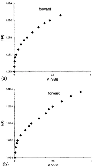
in which A is the contact area, A* is the Richardson constant ( 120 A / ( K 2 cm 2) ), % is the junction barrier height and n is the diode ideality factor. At a given temperature the value of n can be obtained from the slope of the semilogarithmic I - V plot and it must be unity for an ideal diode. The typical l n ( 1 ) - V variations of In/composite/Pt and A1/composite/Pt Schottky devices for the film conductivity of 0.1 S/sin are shown in Fig. 6(a) and (b), respectively. As illustrated in the figures In(I) varies linearly with voltage in the voltage range 0.1 < V< 0.4 V. The deviations from linearity at low bias voltages are due to the shunt resistance and at high voltages (V> 0.4 V) are due to the series resistance effect.
Extrapolation of the linear part of the semilogarithmic plots to zero bias yielded saturation current Io from which the
222 A. Bozkurt etal./Synthetic Metals 87 (1997) 219-223 1,0Eo4 1.0E-5 A ' ~ 1.0E-6 1 . 0 E - 7 1.0E-8
(a)
I) forward I) 0,5 v (volt) Table 1Some parameters of In/composite/Pt and A1/composite/Pt Schottky barrier devices
In/composite/Pt InlcompositelPt (first system) (second system)
I• (A) 5 × 10 -6 1.78× 10 -7
n 9.6 5.2
(eV) 0.64 0.72
o- (Slcm) = l = 1
In/composite/Pt Altcomposite/Pt (second system) (second system) I• (A) 1.25 × 10 -7 7.94× 10 -8 n 2.94 2.64 (eV) 0.74 0.75 o" ( S / c m ) =0.1 =0.1 1.0E-4 1.0'=-5 A 1+0E-6 I +OE-7 ~. 1,0E-S 0
Co)
forward 0,5 1 v (Vott)Fig. 6. Semilogarithmic plots of current vs. forward voltage for (a) In/ composite/Pt and (b) A1/c0mposite/Pt junctions (second system, or= 0.1 S/cm).
barrier height values were determined using Eq. (2). The diode parameters (n, %, Io) of different metal/composite/ Pt structures are tabulated in Table 1. The diode ideality factor values indicate that the junctions fabricated with the high conductivity composite films (1 S / c m ) deviate significantly from ideal Schottky barrier theory and the ones fabricated with lower conductivities have better diode parameters. All the determined values of n are greater than unity. This is probably due to the presence of a thick interfacial layer and/or recombination in the depletion region which will be investi- gated in detail as a further study. Even though the determi- nation of the barrier heights from I - V characteristics is reliable for low n = 1 values, the calculated barrier height values are comparable to the ones in the literature [ 10,12].
In the planar configurations where Au and low work func- tion metals evaporated on the same surface of the composite films, a non-rectifying behavior was observed regardless of the conductivities of the films. This result is probably due to t h e d i f f e r e n c e b e t w e e n t h e p l a n a r a n d p e r p e n d i c u l a r c o n d u c - tivities. It was reported that in PPy the parallel resistivity is
In/composite/Pt A1/composite/Pt (second system) (second system) I• (A) 2.5 × 10 - s 3.1 X I0 -7
n 2.3 2.1
~% (eV) 0.77 0.72
(S/cm) =0.01 =0.01
In/composite/Pt A1/composite/Pt (first system) ( first system)
I• ( A ) 5 X I0 -8 8.3 X 10 . 7
n 2.3 2.24
% (eV) 0.76 0.7
o" (S/cm) =0.01 =0.01
three orders of magnitude lower than the perpendicular resis- tivity [ 16].
.We have measured the room-temperature C-Vdependence of the samples prepared by the second system (A1/compo- site/Pt) at 1 MHz. The capacitance is found to decrease with increasing reverse bias with an increasing rate at high reverse bias voltages. The C - a versus V plot illustrated in Fig. 7 shows a nonlinear variation which indicates a nonuniform dopant density profile with lower concentration in the bulk than the interface. This nonlinearity may also be attributed to
2.5 ,,-, b t.5 ° ° ° o o •
° ° e ~ ° ° e•oo • o o l I~l,n~eo o o o•4b
I I
-2 0
VOLTAGE (v)
Fig. 7. C-2-V variation of A1/composite/Pt junction (second system. o- = 0.1 S/cm).
A: Bozkurr et at./Synthetic Metals 87 (1997) 219-223 223
the variation o f the effective area of the diode with bias which is the result o f the surface irregularities [ 17 ]. C - 2 becomes almost i n d e p e n d e n t o f the a p p l i e d bias at around - 1.5 V which is p r e s u m a b l y due to the insulating layer formed at the surface o f the conducting p o l y m e r prepared by the second system limiting the capacitance at lower r e v e r s e b i a s voltages. Similar C - a - V behavior has been obtained for m e t a l / p o l y - mer contacts by melt processing which was attributed to the additional constant capacitance due to the insulating oxide layer at the interface in series with the variable space-charge capacitance o f the p o l y m e r [ 18 ].
4. Conclusions
In this w o r k a s a m p l e preparation m o d e l for a m e t a l / c o n - d u c t i n g - c o m p o s i t e / m e t a l was suggested. Charge transport limitation was observed between low work function metals (In, A1), and no charge transport limitation was recorded for high w o r k function metals. It was proved that the rectification becomes better as the conductivity o f the composite films decreased, In order to solve the pinhole short problem and obtain films with g o o d surface m o r p h o l o g y we produced P P y / P I n c o m p o s i t e films in which the P P y content was about 80%.
Acknowledgements
This work is partially supported by Grants DPT 95K- 12049 8 and T B A G - 1422.
References
[1] O. Niwa and T. Tamamura, J. Chem. Soc., Chem. Commun., (1984) 817.
[2] B. Zinger and D. Kijel, Synth. Met., 41--43 ( t99t ) 1013. [3] G.P. Zhang and X. Bi, Synth. Met., 41--43 (1991) 251. [4] B. Tieke and W. Gabriel, Polymer, 31 (1990) 20.
[5] Y. Chen, R. Qian, G. Li and Y. Li, Polym. Commun., 32 (1991) 189. [6] X. Bi and Q. Pie, Synth. Met., 22 (1987) 145.
[7] S. Dogma, U. Akbulut mad L. Toppare, Synth. Met., 53 (1992) 29. [8] F. Selampinar, U. Akbulut, T. Yalcin, S. Suzer mad L. Toppare, Synth.
Met., 62 (1994) 201.
[9] H.L. Wang, L. Toppare and J.E. Fernandez, Macromolecutes, 23 (1990) 1053.
[ 10] H. Koezuka and S. Etoh, Jr. Appl. Phys., 54 (1983) 2511.
[11] J.W. Gardener and T.T. Tan, J. Phys.: Condens. Matter, i (1989) SB133.
[ 12] J. Unsworth, Z. Jin, B.A. Lunn and P.C. Innis, Polym. Int., 26 ( 1991 ) 245.
[ 13] O. Ingan/is and L Landstr6m, Synth. Met., 10 (1984/85) 5. [ 14] A. Bozkurt, U. Akbulut and L. Toppare, Synth. Met., 82 (1996) 41. [ 15] S.M. Sze, Physics of Semiconductor Devices, Wiley, New York, 1981. [ t6] E, Garcia-Camarero, F. Arjona mad C. Guillen, J. Mater. Sci., 25
(1990) 4914.
[ 17] A.M. Goodmann, J. Appl. Phys., 34 ( 1963 ) 329.
[ 18] M. Sundberg, G. Gustafsson mad O. Ingmagts, Appl. Phys. Lett., 57 (1990) 733.