Plasmonic backcontact grating for P3HT:PCBM
organic solar cells enabling strong optical
absorption increased in all polarizations
Mustafa Akin Sefunc,* Ali Kemal Okyay, and Hilmi Volkan Demir Department of Electrical and Electronics Engineering, Department of Physics, UNAM - National Institute ofMaterials Science and Nanotechnology, Bilkent University, Ankara 06800, Turkey
School of Electrical and Electronic Engineering, Microelectronics Division; School of Physical and Mathematical Sciences, Physics and Applied Physics Division, Nanyang Technological University, 639798 Singapore
Abstract: In P3HT:PCBM based organic solar cells we propose and demonstrate numerically plasmonic backcontact grating architectures for strong optical absorption enhanced in both transverse-magnetic and transverse-electric polarizations. Even when the active material is partially replaced by the metallic grating (without increasing the active layer film thickness), we show computationally that the light absorption in thin-film P3HT:PCBM is increased by a maximum factor of ~21% considering both polarizations under AM1.5G solar radiation and over a half-maximum incidence angle of 45° (where the enhancement drops to its half) compared to the same cell without a grating. This backcontact grating outperforms the typical plasmonic grating placed in PEDOT:PSS layer.
©2011 Optical Society of America
OCIS codes: (250.5403) Plasmonics; (240.6680) Surface plasmons; (050.2770) Gratings;
(040.5350) Photovoltaic; (350.6050) Solar energy.
References and links
1. P. A. Troshin, H. Hoppe, J. Renz, M. Egginger, J. Y. Mayorova, A. E. Goryachev, A. S. Peregudov, R. N. Lyubovskaya, G. Gobsch, N. S. Sariciftci, and V. F. Razumov, “Material solubility-photovoltaic performance relationship in the design of novel fullerene derivatives for bulk heterojunction solar cells,” Adv. Funct. Mater.
19(5), 779–788 (2009).
2. T. Ameri, G. Dennler, C. Lungenschmied, and C. J. Brabec, “Organic tandem solar cells: A review,” Energy Environ. Sci. 2(4), 347–363 (2009).
3. D. Duche, E. Drouard, J. Simon, L. Escoubas, P. Torchio, J. L. Rouzo, and S. Vedraine, “Light harvesting in organic solar cells,” Sol. Energy Mater. Sol. Cells 95(1), 18–25 (2011).
4. C. Min, J. Li, G. Veronis, J. Lee, S. Fan, and P. Peumans, “Enhancement of optical absorption in thin-film organic solar cells through the excitation of plasmonic modes in metallic gratings,” Appl. Phys. Lett. 96(13), 133302 (2010).
5. S. J. Tsai, M. Ballarotto, D. B. Romero, W. N. Herman, H. C. Kan, and R. J. Phaneuf, “Effect of gold nanopillar arrays on the absorption spectrum of a bulk heterojunction organic solar cell,” Opt. Express 18(S4 Suppl 4), A528–A535 (2010).
6. A. P. Kulkarni, K. M. Noone, K. Munechika, S. R. Guyer, and D. S. Ginger, “Plasmon-enhanced charge carrier generation in organic photovoltaic films using silver nanoprisms,” Nano Lett. 10(4), 1501–1505 (2010). 7. H. Shen, P. Bienstman, and B. Maes, “Plasmonic absorption enhancement in organic solar cells with thin active
layers,” J. Appl. Phys. 106(7), 073109 (2009).
8. H. Hoppe, N. S. Sariciftci, and D. Meissner, “Oprical constants of conjugated polymer/fullerene based bulk-heterojunction organic solar cells,” Mol. Cryst. Liq. Cryst. (Phila. Pa.) 385(1), 113–119 (2002).
9. H. A. Atwater and A. Polman, “Plasmonics for improved photovoltaic devices,” Nat. Mater. 9(3), 205–213 (2010).
10. H. Sai, H. Fujiwara, and M. Kondo, “Back surface reflectors with periodic textures fabricated by self-ordering process for light trapping in thin-film microcrystalline silicon solar cells,” Sol. Energy Mater. Sol. Cells 93(6–7), 1087–1090 (2009).
11. V. E. Ferry, L. A. Sweatlock, D. Pacifici, and H. A. Atwater, “Plasmonic nanostructure design for efficient light coupling into solar cells,” Nano Lett. 8(12), 4391–4397 (2008).
12. R. A. Pala, J. White, E. Barnard, J. Liu, and M. L. Brongersma, “Design of plasmonic thin-film solar cells with broadband absorption enhancements,” Adv. Mater. (Deerfield Beach Fla.) 21(34), 3504–3509 (2009). 13. N. C. Panoiu and R. M. Osgood, Jr., “Enhanced optical absorption for photovoltaics via excitation of waveguide
14. V. E. Ferry, M. A. Verschuuren, H. B. T. Li, E. Verhagen, R. J. Walters, R. E. I. Schropp, H. A. Atwater, and A. Polman, “Light trapping in ultrathin plasmonic solar cells,” Opt. Express 18(S2 Suppl 2), A237–A245 (2010). 15. V. E. Ferry, M. A. Verschuuren, H. B. T. Li, R. E. I. Schropp, H. A. Atwater, and A. Polman, “Improved
red-response in thin film a-Si:H solar cells with soft-imprinted plasmonic back reflectors,” Appl. Phys. Lett. 95(18), 183503 (2009).
16. W. Bai, Q. Gan, F. Bartoli, J. Zhang, L. Cai, Y. Huang, and G. Song, “Design of plasmonic back structures for efficiency enhancement of thin-film amorphous Si solar cells,” Opt. Lett. 34(23), 3725–3727 (2009).
17. S. Mokkapati, F. J. Beck, A. Polman, and K. R. Catchpole, “Designing periodic arrays of metal nanoparticles for light-trapping applications in solar cells,” Appl. Phys. Lett. 95(5), 053115 (2009).
18. F. J. Beck, S. Mokkapati, A. Polman, and K. R. Catchpole, “Asymmetry in photocurrent enhancement by plasmonic nanoparticle arrays located on the front or on the rear of solar cells,” Appl. Phys. Lett. 96(3), 033113 (2010).
19. I. Diukman, L. Tzabari, N. Berkovitch, N. Tessler, and M. Orenstein, “Controlling absorption enhancement in organic photovoltaic cells by patterning Au nano disks within the active layer,” Opt. Express 19(S1 Suppl 1), A64–A71 (2011).
20. M. A. Sefunc, A. K. Okyay, and H. V. Demir, “Volumetric plasmonic resonator architecture for thin-film solar cells,” Appl. Phys. Lett. 98(9), 093117 (2011).
21. J. A. Schuller, E. S. Barnard, W. Cai, Y. C. Jun, J. S. White, and M. L. Brongersma, “Plasmonics for extreme light concentration and manipulation,” Nat. Mater. 9(3), 193–204 (2010).
22. W. L. Barnes, A. Dereux, and T. W. Ebbesen, “Surface plasmon subwavelength optics,” Nature 424(6950), 824– 830 (2003).
23. P. Peumans, S. Uchida, and S. R. Forrest, “Efficient bulk heterojunction photovoltaic cells using small-molecular-weight organic thin films,” Nature 425(6954), 158–162 (2003).
24. X. Chen, C. Zhao, L. Rothberg, and M. Ng, “Plasmon enhancement of bulk heterojunction organic photovoltaic devices by electrode modification,” Appl. Phys. Lett. 93(12), 123302 (2008).
25. D. W. Zhao, P. Liu, X. W. Sun, S. T. Tan, L. Ke, and A. K. K. Kyaw, “An inverted organic solar cell with an ultrathin Ca electron-transporting layer and MoO3 hole-transporting layer,” Appl. Phys. Lett. 95(15), 153304
(2009).
26. H. Kitami, T. Sakai, T. Hishinuma, A. Sanda, H. Kusano, and M. Kitagawa, “Widening of harvesting layer and are of P3HT/PCBM bulk-heterojunction photovoltaic cells,” Sol. Energy Mater. Sol. Cells 95(1), 357–360 (2011).
27. E. D. Palik, ed., Handbook of Optical Constants of Solids (Academic, 1985).
28. F. Monestier, J.-J. Simon, P. Torchio, L. Escoubas, F. Flory, S. Bailly, R. de Bettignies, S. Guillerez, and C. Defranoux, “Modeling the short-circuit current density of polymer solar cells based on P3HT:PCBM blend,” Sol. Energy Mater. Sol. Cells 91(5), 405–410 (2007).
29. K. R. Catchpole and A. Polman, “Design principles for particle plasmon enhanced solar cells,” Appl. Phys. Lett.
93(19), 191113 (2008).
1. Introduction
Organic solar cells (OSCs) attract both scientific and industrial attention because of competitive advantages they offer for production at low cost and with high throughput. However, despite these strategic benefits, the solar conversion efficiency of OSCs may be low in thin-film architectures when compared to high-end inorganic counterparts. This is mainly due to the trade-off between light absorption and exciton diffusion [1–3]. Photogenerated excitons (bound electron-hole pairs) can diffuse only over very limited lengths (in the order of tens of nanometers), which can severely limit charge collection. Therefore, the absorbing layers may need to be thin enough [1–7]. Depending on the device design, the optical absorption may not be sufficiently strong as a result. In that case, low solar conversion efficiency in such very thin active layers becomes one of the major challenges. To date there have been a significant number of reports on high performance organic materials which can be utilized in the fabrication of such OSCs (e.g., [1,2,8]). In recent years, bulk heterojunction OSCs based on P3HT:PCBM (one-to-one ratio mixture of poly-3-hexylthiophene and phenyl-C61-butyric acid methyl ester) active material have received much interest owing to their large absorption [1]. In addition to the research efforts on highly absorptive organic materials, new OSC designs that enable surface plasmon resonance (SPR) excitation have been proposed and demonstrated to enhance total optical absorption [4–7,9–20].
In the literature, various plasmonic solar cell strategies have been studied. In these prior reports, generally three ways of enhancing the optical absorption in solar cells have been extensively investigated: metallic nanoparticles or periodic structures integrated on top of the
the backcontact surface to use surface plasmon polaritons excited at metal/dielectric interface [9–11,14–16]. Recently, metallic grating architectures on backcontact of silicon-based solar cells have also been demonstrated to enhance total optical absorption under transverse-magnetic (TM) polarized illumination [9,10,16]. Furthermore, increased absorption via a nanoimprinted pattern of holes on the backcontact surface has been investigated in a-Si:H solar cell [14,15]. In P3HT:PCBM based OSCs, however, only the metallic nanoparticles mixed with absorbing materials have been accomplished to enhance optical absorption till date. Incorporation of such engineered metallic architectures on backcontact of these OSCs and their parametric studies have not been reported to date.
In addition, the effect of illumination polarization on the optical absorption has not previously been considered in the prior reports. In the previous literature, one polarization of illumination may lead to strong field localization in the active material because of the excitation of plasmon modes [4,13,16,21,22], while the other polarization may, however, yield weak localization. In some cases one may even observe reduced absorption in the other polarization. On the other hand, the incoming and scattered sunlight are not specifically polarized and includes both transverse-electric (TE) and TM polarizations. Thus, designing a proper plasmonic geometry that simultaneously enhances the optical absorption considering both TE- and TM-polarized illumination is essential for the future of plasmon assisted organic solar cells.
In this paper, we present surface plasmon polariton assisted thin-film organic solar cells made of P3HT:PCBM based on plasmonic backcontact grating architecture for enhancing optical absorption under TM- and TE-polarization within the most effective spectral range of AM1.5G solar radiation. Using finite-difference time-domain (FDTD) simulations, we investigate and understand the effect of metallic gratings on near-field localization and the resulting enhanced optical absorptivity in the plasmonic OSC structures. We further study and identify the effect of incidence angle variation on the total absorptivity and the resulting plasmonic enhancement reduction.
2. Structure and Simulation Details
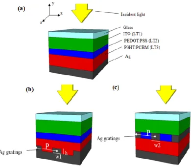
In our study, we analyzed two plasmonic structures embedded into the organic solar cell architecture comprised of glass/ITO/PEDOT:PSS/P3HT:PCBM/Ag and compared their absorptivity performance with the case of a bare device in the same architecture without a grating to identify the enhancement of the proposed plasmonic resonators. The device structure details are given as follows: A thick metal contact cathode layer covers a 100 nm thick absorbing layer of active material blend, P3HT:PCBM. Subsequently, a 50 nm thick PEDOT:PSS (one-to-one ratio mixture of poly (3,4-ethylenedioxythiophene) and poly (styrenesulfonate)) layer is used for the hole transportation in the device. A transparent 150 nm thick ITO (indium-tin-oxide) anode layer is followed on top of the PEDOT:PSS layer for providing an electrical contact from the organic solar cell. The metal grating is chosen to be made of Ag in our studies. In the literature, a low workfunction metals (e.g., Al, Ca, Mg, Ag) are used as the cathode layer for electron collection in different types of solar cells [1– 3,9,14,15,23]. Especially, Al, LiF/Al and Ca/Ag are generally embodied as the backside contact layer in P3HT:PCBM based solar cells because of their matching workfunctions [1,24,25]. A P3HT:PCBM bulk heterojunction solar cell has also been accomplished with silver cathode layer alone without using any additional electron transport layer [26]. To date, the reported plasmon assisted solar cell designs generally consist of silver structures to generate surface plasmon resonances [9,14,15]. In this paper, to produce the required surface plasmon resonances, we also selected the cathode layer and top metal gratings in silver. A transparent glass substrate (refractive index n~1.52) is used to provide mechanical support for these thin-film layers spun on it. The schematic view of this solar cell architecture is illustrated in Fig. 1(a).
Fig. 1. Cross-sectional view of the thin-film organic solar cell (OSC) architecture made of glass/ITO/PEDOT:PSS/P3HT:PCBM/Ag: (a) the bare (non-metallic architecture) thin-film OSC as a reference sample (Here LT stands for the corresponding layer thickness.), (b) OSC with the bottom grating, (P indicates the period, w1 denotes the width, and h represents the height of the bottom grating.), and (c) OSC with the top grating (w2 indicates the width of the top grating.). In our simulations, the illumination is set to be normal to the device structure and the architecture is assumed to be infinite along x- and z-axes.
We performed 2-dimensional finite-difference time-domain (FDTD) simulations to compute the optical absorption in different devices structures, and understood the absorption enhancement contribution of plasmonic architectures embedded into the solar cell. In our computations we use experimentally measured complex dielectric constants of Ag [27], P3HT:PCBM [28], PEDOT:PSS [8] and ITO [8] layers with no approximation. All of the investigated organic solar cells structures here are illuminated by a plane-wave incident through the glass, which is set normal to the cell structure, as illustrated in Fig. 1.
Periodic boundary conditions are set along the x-axis (xmax and xmin) and perfectly matched layer (PML) boundaries are set along the y-axis (ymax and ymin). The absorption spectra are calculated in the active P3HT:PCBM layer in the spectral range of 400 to 800 nm. This wavelength range covers most of the solar radiation spectrum and the effective absorption region of P3HT:PCBM active material. To compute the field intensity enhancement in the structure, we use Eq. (1). The optical absorption spectrum at a given wavelength is given by Eq. (2), where E is the electric field, V is volume of the material, and Im( )
is the dielectric constant of the material of which absorption will be calculated.2 , 2 | | | | top bottom V bare V E dV E dV
(1) 2 * Im( ) | | V A
E dV (2)AM1.5G solar radiation, which is commonly used in photovoltaic device characterization, mimics the radiation of the sun. It is important to calculate the enhancement factors under AM1.5G to identify the contribution of plasmonic architecture. The overall absorption is given by the average of absorptivity under both TE- and TM-polarized illumination, i.e., (ATM + ATE)/2. We compute the performance enhancement of the plasmonic solar cell architecture (in %) under AM1.5G solar radiation by using Eq. (3).
800 800 400 400 800 400 ( ) ( ) ( ) 1.5 ( ) ( ) 1.5 ( ) 2 100 ( ) 1.5 ( ) nm nm TM TE bare nm nm nm bare nm A A AM G d A AM G d A AM G d
(3)3. Simulation Results, Analyses and Discussion
The first investigated plasmonic architecture is the bottom grating architecture. This structure consists of periodic gratings placed on top of the cathode layer. The cross-sectional view of the corresponding plasmonic architecture is presented in Fig. 1(b). In this architecture, some of the active material is replaced by the metallic grating. We do not add any active material here to compensate for the removed active material; the active material thickness is fixed to 100 nm in all cases. The second plasmonic architecture, which we considered for comparison purposes, is the top grating embedded in the organic solar cell device, as shown in Fig. 1(c). In this architecture, the hole transport layer (PEDOT:PSS layer) is partially substituted by the periodic grating. Such a top periodic grating structure has been widely studied in the previous literature [4,9,12,13,17–19,29]. Here we simulate and compare our proposed plasmonic architecture of patterned backcontact with this well-studied top grating architecture to identify the performance enhancement contribution of our plasmonic architecture located on the bottom.
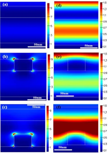
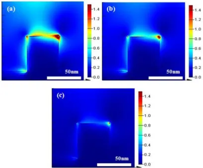
Fig. 2. Electric field (|E|2) maps at λ = 600 nm under TM illumination for (a) the bare
(reference) structure consisting of glass/ITO/PEDOT:PSS/P3HT:PCBM/Ag, (b) the top grating structure – partially substituting the PEDOT:PSS layer with Ag periodic gratings, and (c) the Ag bottom grating case – adding periodic grating on top of backcontact – and under TE illumination for (d) the bare, (e) the top grating, and (f) the bottom grating structure for parameters of P = 130 nm, LT1 = 150 nm, LT2 = 50 nm, LT3 = 100 nm, w1 = 50 nm, w2 = 50 nm and h = 50 nm. Here one unit cell of the repeating grating structure is used to visualize the electric field maps.
Figure 2(a) shows the field profiles generated in the bare (non-metallic) architecture under TM-polarized illumination. The field intensity in the volume of the active material is slightly higher compared to other layers. Figure 2(b) presents the electric field map of the top grating architecture under TM-polarized at λ = 600 nm. We observe in Fig. 3(a) that the absorptivity performance of the top grating based architecture is lower than that of the bare architecture. The field profiles show that the top metallic gratings reflect the incoming light, and this reflection causes a decrease in the absorption of the active material. Figure 2(c) clearly proves the surface plasmons generated around the bottom metallic gratings (represented as high field intensities in the color map), which are localized in the active material. The opposite surface of the grating applies an effective restoring force on the present free electrons in the metal. Therefore, a resonance that leads to a field localization can form around the corners of the metallic grating. The localized surface plasmons that are non-propagating excitations of the conduction electrons of the metallic structure are observed around the bottom metallic grating.
material interface increases the absorptivity of the active materials since the absorptivity is linearly proportional to the intensity (electric field square) in the volume of the active material. These improvements are indicated in the absorption spectra of Fig. 3(a).
Figure 2(d) depicts the field profile generated in the bare (non-metallic) architecture under TE-polarized illumination. Here also the field intensity in the volume of the active material is slightly stronger than the other layers. Figure 2(e) shows the electric field intensity behavior of the top grating architecture under TE-polarized illumination at λ = 600 nm. As observed in Fig. 3(b), the absorptivity performance is lower than that of the bare architecture. The field map demonstrates that the top metallic gratings reflect the incoming light, which decreases the optical absorption of the active material. Figure 2(f) presents the electric field profile for the bottom grating architecture. The change in Fabry-Perot resonance in absorbing material leads to strong field amplification because of introducing a nanopatterned metallic surface (bottom grating). The refractive index difference between the P3HT:PCBM (n ~1.45 at λ = 600 nm) and PEDOT:PSS (n ~2.1 at λ = 600 nm) layers causes total internal reflection, thus the light is trapped in the P3HT:PCBM active layer.
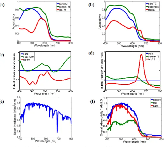
Fig. 3. Calculated absorption spectra of the organic active material in the bare, bottom grating, and top grating structures computed for the device parameter of P = 130 nm, LT1 = 150 nm, LT2 = 50 nm, LT3 = 100 nm, w1 = 50 nm, w2 = 50 nm, and h = 50 nm under (a) TM-polarized (Media 1) and (b) TE-polarized light illumination (Media 2). Electric field intensity enhancement within the volume of the organic active material using the bottom grating (given in Fig. 1(b)) and the top grating (given in Fig. 1(c)) structures compared to that generated in the bare structure, with this field enhancement shown for (c) TM-polarized and (d) TE-polarized light illumination. (e) Air mass (AM) 1.5G solar radiation. (f) Multiplication of AM1.5G solar radiation and overall absorptivity in the volume of the organic active material in the bare, bottom grating, and top grating structures.
Figure 3(c) and Fig. 3(d) present the electric field intensity (electric field square) enhancement in the volume of active layer in the bottom and top grating architectures in comparison to the electric field in the bare structure. Figure 3(c) shows that we enhance the electric field in the 400-800 nm region, except for small spectral ranges of 450-480 nm and 650-700 nm under TM-polarized illumination. In the 400-800 nm range, the electric field is boosted up to 1.7 folds by placing the bottom plasmonic structure. However, the top grating architecture reduces the electric field in the active material. This condition causes to decrease the overall absorption as observed in Fig. 3(a). Figure 3(d) shows that we enhance the electric field in the 400-650 nm region under TE-polarized illumination. In this range, the electric field is enhanced up to 1.4 folds with the bottom grating structure. The top grating architecture reduces the electric field intensity in the active material except for the enhancement in 630-700 nm range. In this range, the allowed waveguide modes at these frequencies leads to the localized surface plasmons located at the bottom of the top grating. The normalized field map of the top grating structure is given in Fig. 2(f). This field localization at these frequencies enhances the absorptivity in this wavelength range as shown in Fig. 3(b).
Fig. 4. Map of absorptivity in the active layer of (a) the bottom grating structure under TM, (b) the bottom grating structure under TE, (c) the top grating structure under TM and (d) the top grating structure under TE. The absorption spectra are shown for parameters of w1 = 50 nm, h1 = 50 nm, LT1 = 150 nm, LT2 = 50 nm and LT3 = 100 nm.
We also considered the effect of grating periodicity on the absorptivity under both TE- and TM-polarized illumination. The absorptivity vs. periodicity maps of the bottom grating structure under TM-polarized illumination, bottom grating structure under TE-polarized illumination, top grating structure under TM-polarized illumination and top grating structure under TE-polarized illumination are given in Fig. 4(a), Fig. 4(b), Fig. 4(c) and Fig. 4(d), respectively. All absorptivity vs. periodicity maps are normalized in the absorptivity range of 0-1. The absorptivity behavior of the bottom grating embedded architecture remains almost the same in the period range of 100-350 nm. For long periodicities, the absorptivity tends to decrease and match the absorptivity of the bare structure since the large field enhancement via excited surface plasmon modes per volume decreases and the plasmonic excitation behavior becomes insignificant. The top grating architecture has the lowest absorptivity behavior at
architecture also increases since the top metallic grating stops reflecting and allows for more light to couple into the active material. Figure 5 presents the resulting multiplication of the overall absorption of (ATM + ATE)/2 with AM1.5G solar spectrum.
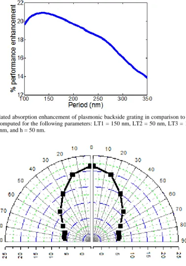
Fig. 5. Calculated absorption enhancement of plasmonic backside grating in comparison to the bare device computed for the following parameters: LT1 = 150 nm, LT2 = 50 nm, LT3 = 100 nm, w1 = 50 nm, and h = 50 nm.
Fig. 6. Effect of the incidence angle on calculated overall total absorption enhancement in the plasmonic backcontact grating architecture. All device parameters are the same as those in Fig. 2.
The backcontact grating design exhibits improved enhancement levels compared to the top grating structure and the bare device for surface-normal configuration. In Fig. 6, we investigate how much the performance enhancement factor is reduced as the angle of incidence is increased from surface normal towards off-axis angles for the backcontact design. According to these simulations, the resulting absorption enhancement is relatively weak depending on the angle of incidence for the range of small angles in the case of the backcontact grating design. However, the optical absorption in the active layers further decreases with the increasing angle due to depleted localized SPRs around the metallic gratings. When the angle of incidence is increased, the light travels a longer way in the active material until it hits the metallic gratings on the backcontact surface. Thus, this reduces the intensity of the light, which results in weak surface plasmons and reduced field localizations around the metallic surfaces. We find out that the enhancement in the optical absorption of thin-film P3HT:PCBM drops to this half-maximum at an incidence angle of 45° compared to the same cell without a grating. The effect of incident angle on electric field distributions is depicted in Fig. 7 for large off-axis angles. In backcontact grating architecture, we do not add
any active material to compensate for the removed active material replaced by the metallic grating. However, the effect of removed active material becomes significant for large off-axis angles.
Fig. 7. Effect of the incidence angle on field distribution (|E|2) in backcontact grating architecture at λ = 400 nm under TM-polarized illumination. Field distributions are given at illumination angles (a) 70° (b) 75°, and (c) 80°. All device parameters are the same as those in Fig. 2.
4. Conclusion
In conclusion, we proposed and demonstrated numerically metallic grating backcontact structure that enables strong optical absorption in P3HT:PCBM based solar cells enhanced in all polarization for the first time. We modeled and simulated the performance of plasmonic architectures under both TE- and TM-polarized illumination and also presented the parametric study results for this device structure. By taking advantage of generated surface plasmon polaritons near metal/dielectric interface, we found out a plasmon assisted absorption increase up to ~21% in the active layers of this solar cell under TE- and TM-polarizations even when we effectively reduce the active material by replacing it with metallic gratings. The optical absorption enhancements occur in the most effective range of spectral distribution of sunlight (in 450-600 nm range). Plasmon enhanced absorption proposed in this work proves to be a promising approach to increase the performance of commonly used organic solar cells of P3HT:PCBM. This design strategy can potentially be extended to 3-dimensional metallic structures and different kinds of solar cell architectures.
Acknowledgments
This work is supported by EU-FP7 Nanophotonics4Energy NoE, and TUBITAK Grant Nos. EEEAG 109E002, 109E004, 110E010, and 110E217. H.V.D. acknowledges support from ESF-EURYI and TUBA GEBIP.