SOLUTION-PROCESSED
NANOSTRUCTURES AND DEVICES FOR
HIGHLY POLARIZED LIGHT
GENERATION, SCATTERING AND
SENSING
a dissertation submitted to
the graduate school of engineering and science
of bilkent university
in partial fulfillment of the requirements for
the degree of
doctor of philosophy
in
electrical and electronics engineering
By
Can Uran
December, 2014
SOLUTION-PROCESSED NANOSTRUCTURES AND DEVICES FOR HIGHLY POLARIZED LIGHT GENERATION, SCATTERING AND SENSING
By Can Uran December, 2014
We certify that we have read this thesis and that in our opinion it is fully adequate, in scope and in quality, as a dissertation for the degree of Doctor of Philosophy.
Assoc. Prof. Dr. Hilmi Volkan Demir (Advisor)
Prof. Dr. Ayhan Altınta¸s
Assist. Prof. Dr. Ali Kemal Okyay
Assoc. Prof. Dr. D¨on¨u¸s Tuncel
Assist. Prof. Dr. Evren Mutlug¨un Approved for the Graduate School of Engineering and Science:
Prof. Dr. Levent Onural Director of the Graduate School
ABSTRACT
SOLUTION-PROCESSED NANOSTRUCTURES AND
DEVICES FOR HIGHLY POLARIZED LIGHT
GENERATION, SCATTERING AND SENSING
Can Uran
Ph.D. in Electrical and Electronics Engineering Advisor: Assoc. Prof. Dr. Hilmi Volkan Demir
December, 2014
Recent advancements in photonics have facilitated robust and reliable light sources, displays and photosensors with relatively long lifetimes and high energy efficiency in their classes. However, developing intrinsically polarization selec-tive photonic devices still remains a challenge, although polarization sensitivity is essential to various advanced functions and/or improved performance. One of the main difficulties in making such devices emerges from the compromise on the efficiency while striving to reach high polarization contrast levels. For instance, commercially available birefringent structures including those integrating liquid crystals suffer from major transmission losses. On the other hand, solution-processed, high aspect-ratio nanostructures may offer power efficient platforms with high polarization contrasts via selection of the polarization in a preferred direction during emission, absorption and/or scattering process(es) while sup-pressing efficiency of the relevant ones in the other polarization. In this thesis, we present solution-processed metal and semiconductor nanostructures and op-toelectronic devices made from them for highly polarized light generation and enhanced photosensing. Here we developed and demonstrated in-template fabri-cated suspended arrays of plasmonic thin nanodiscs with tunable disc-heights and gap-widths tailoring absorption and scattering properties for applications ranging from polarized light scattering to photodetection. Also, we proposed and showed highly polarized light emission in coupled thin films of magnetically aligned multi-segmented nanowires and colloidal nanocrystals for polarized color enrichment in displays. Here well-controlled in-template synthesis of these nanowires together with their alignment under magnetic field allows for highly parallel orientation of the nanowires in massive numbers over large-area thin films. Integrating with color-enriching nanocrystals, this enabled a record high polarization contrast over 15:1 for the isotropic nanocrystals in the visible range. We believe that such
iv
hybrid assemblies of solution-processed nanostructures integrated into optoelec-tronic devices hold great promise for advanced functions in photonics.
Keywords: Nanowires, nanodiscs, nanocrystals, quantum dots, plasmonic nanos-tructures, polarization contrast, light generation, scattering, photosensing.
¨
OZET
Y ¨
UKSEK POLAR˙IZE IS
¸IMA, SAC
¸ ILMA VE
ALGILAMA ˙IC
¸ ˙IN SOL ¨
USYON BAZLI ˙IS
¸LENM˙IS
¸
NANOYAPILAR VE AYGITLAR
Can Uran
Elektrik ve Elektronik M¨uhendisli˘gi, Doktora Tez Danı¸smanı: Assoc. Prof. Dr. Hilmi Volkan Demir
Aralık, 2014
Fotonikteki son geli¸smeler, kendi sınıflarında daha uzun ¨om¨url¨u, y¨uksek enerji ver-imli ve g¨uvenilir ı¸sık kaynaklarına, ekranlara ve fotosens¨orlere imkan sa˘glamı¸stır. Ancak, polarizasyon duyarlılı˘gı bir¸cok geli¸smi¸s fonksiyon ve/veya performans i¸cin gerekli olmasına ra˘gmen, polarizasyon se¸cici fotonik aygıtlar geli¸stirmek hala bir sorun olmaya devam etmektedir. Bu t¨ur cihazların yapımındaki ana zorluk-lardan biri y¨uksek polarizasyon kontrast seviyelerine ula¸smaya ¸calı¸sırken enerji verimlili˘gindeki verilen ¨od¨unden kaynaklanır. Orne˘¨ gin, mevcut sıvı kristaller ile entegre ¸cift kırılımlı yapılar, ı¸sık iletiminde b¨uy¨uk kayıplar g¨osterirler. ¨Ote yandan, sol¨usyon bazlı i¸slenmi¸s ve y¨uksek en boy oranına sahip nanoyapılar, ı¸sıma, so˘gurma ve sa¸cılım sırasında tercih edilen bir y¨onde yapılan polarizasyon se¸cimi ile y¨uksek polarizasyon oranlı ve aynı zamanda enerji verimli platform-lar sunabilir. Bu yapıplatform-lar, s¨oz¨u edilen mekanizmalarla bir y¨ondeki polarizasy-onu se¸cici olarak ge¸cirirken di˘ger y¨ondeki polarizasyonu da bastırmaktadır. Bu tezde sol¨usyon tabanlı i¸slenmi¸s metal ve yarı iletken nanoyapıları ve bunlarla yapılan y¨uksek derece polarize ı¸sık ¨ureten ve artırılımı¸s fotoalgılama yapan op-toelektronik aygıtlar sunuyoruz. Burada, ¸sablonda sentezlenen, disk y¨ukseklikleri ve aralık geni¸slikleri ile so˘gurma ve sa¸cılım ¨ozellikleri ayarlanabilen, havada asılı plazmonik ince nanodisk dizileri ¨uretip g¨osterdik. Ayrıca, manyetik olarak hiza-lanmı¸s ¸cok kısımlı nanotellerin kolloidal nanokristaller ile birle¸stirildi˘gi ince film-ler kullanarak polarize renk zenginle¸stirme uygulamalarında son derece y¨uksek polarize ı¸sıma ¨onerdik ve g¨osterdik. Burda ¸sablon i¸cinde y¨uksek kontroll¨u sen-tezlenen nanotellerin manyetik alan altında dizilimi, ince filmli geni¸s y¨uzeylerde olduk¸ca paralel ve etkili bir y¨onlerdirmeyi m¨umk¨un kılıyor. Dizilmi¸s nanotellerin renk zenginle¸stirici nanokristallerle entegre edilmeleri 15:1in ¨uzerinde, izotropik nanokristaller ile elde edilmi¸s rekor bir g¨or¨un¨ur spektrum polarizasyon kontrastı
vi
sa˘gladı. Bu ¸sekilde sol¨usyon bazlı i¸slenmi¸s nanoyapıların optoelektronik ciha-zlara entegresi ile elde edilen melez olu¸sumlar fotonikte ileri d¨uzeyde i¸slevlerin ger¸cekle¸stirilmesi i¸cin b¨uy¨uk ¨oneme sahiptir.
Anahtar s¨ozc¨ukler : Nanoteller, nanodiskler, nanokristaller, kuvantum nok-tacıkları, plasmonik nanoyapılar, polarizasyon kontrastı, ı¸sık ¨uretimi, sa¸cılma, fotoalgılama.
Acknowledgement
First of all, I would like to thank my supervisor Prof. Hilmi Volkan Demir, who has provided me with the understanding and motivation in both scientific and daily life. His kind, friendly and motivating personality guided me during my study of research and I am honored with his supervision. I thank him again for his endless effort and support. I would like to thank Prof. Ali Kemal Okyay and Prof. D¨on¨u¸s Tuncel for serving on my PhD thesis progress committee. They have carefully followed my studies and contributed with their valuable ideas and comments for my thesis progress. I would also like to thank Prof. Ayhan Altınta¸s and Prof. Evren Mutlug¨un for kindly taking part in my PhD thesis defense jury. I would like to thank all of my friends in our Sensors and Devices Research Group for their great support and unforgettable times together: Shahab Akhavan, Akbar Alipour, Talha Erdem, Zeliha Erdem, Burak G¨uzelt¨urk, Yusuf Kele¸stemur, Kıvan¸c G¨ung¨or, Berkay Bozok, Aydan Yeltik, Neslihan C¸ i¸cek, Tuncay ¨Ozel, ˙Ilkem
¨
Ozge ¨Ozel, Zafer Akg¨ul, Onur Erdem, Mustafa Akın Sef¨un¸c, Onur Akın, ¨Ozg¨un Aky¨uz, Emre ¨Unal, Dr. Emre Sarı, Dr. Murat So˘gancı, Prof. Sedat Nizamo˘glu, Prof. Nihan Kosku Perkg¨oz, Prof. Rohat Melik and Prof. Urartu S¸eker. I would like to thank all UNAM and ARL researchers and staff for their support and help on my experimental studies and for providing me with a well equipped research environment. I would like to thank all EE faculty, technical and administrative staff, researchers, and to my close friends, Emre Kopano˘glu, Aslı ¨Unl¨ugedik, Sıtar Kortik, Duygu S¸atır, G¨ulis Zengin, Refik Sina Toru, Elif Aydo˘gdu, Niyazi S¸enlik, Behnam Ghassemiparvin, Volkan A¸cıkel and Mehmet Can Kerse. I have been really happy to study at my department where I have had very good relations and friendships and at the same time acquire high level of engineering education. Lastly, I would like to thank a lot my parents, my brother and all my family for their support and love.
Contents
1 Introduction 1
2 Background 6
2.1 Semiconductor nanocrystals . . . 6
2.2 An example of semiconductor nanocrystal synthesis . . . 7
2.3 Layer-by-layer assembly of semiconductor nanocrystals . . . 8
2.4 Metal nanoparticles . . . 9
2.5 An example of metal nanoparticle synthesis . . . 10
3 In-template electrodeposited nanostructures 13 3.1 Nanowire synthesis . . . 13
3.2 Nanogap variation study . . . 23
3.3 Suspended and dispersible nanostructures . . . 24
4 Magnetically aligned segmented nanowires integrated with isotropic nanocrystals 30 4.1 Introduction . . . 30
4.2 Results and discussion . . . 32
4.3 Conclusion . . . 41
5 Arrays of suspended plasmonic nanodiscs 42 5.1 Introduction . . . 42
5.2 Results and discussion . . . 43
5.3 Conclusion . . . 54 6 Large-area photosensors of nanocrystals 55
CONTENTS ix
6.1 Introduction . . . 55 6.2 Results and discussion . . . 57 6.3 Conclusion . . . 76
List of Figures
2.1 Semiconductor quantum dots syntesized in our setup. . . 7 2.2 Plasmons inside metal nanoparticles. . . 10 2.3 Our gold nanowires (on the left) and nanoparticles in water (on
the right). As the particle size shrinks smaller than the 50 nm, the color turns reddish due to plasmonic effect. . . 11 2.4 Absorbance spectrum of our gold nanoparticles in film. . . 12 3.1 Our experimental setup for electrodeposition that includes
tem-plate membrane disc, o-ring, and tem-plates. . . 15 3.2 Versastat3 potentiostat/galvanostat. . . 15 3.3 Our experimental setup for electrodes. . . 16 3.4 Potential trace during silver deposition into the branched part of
the alumina disc. . . 17 3.5 Potential trace during silver deposition into the pores of the
alu-mina disc for Ag segments of our nanowires. . . 18 3.6 Potential trace during gold deposition into the pores of the alumina
disc for Au segments of our nanowires. . . 18 3.7 SEM image of the nanowires inside the alumina disc. . . 19 3.8 SEM image of an exemplary nanowire with a short Ag segment in
the middle between long Au segments at the ends (with a total nanowire length of 7.78 µm). . . 20 3.9 SEM image of another nanowire with 3.23 µm and 3.35 µm long
Au segments. . . 20 3.10 In-template electrodeposition process flow . . . 20
LIST OF FIGURES xi
3.11 Backside of the membrane disc (a) before deposition and (b) after silver backing. . . 21 3.12 Silver backing is etched, membrane is dissolved and nanowires are
dispersed inside solution. . . 21 3.13 Nanowire synthesized in track-etched polycarbonate membrane (a)
in full view and (b) with a zoom-in across its width. . . 22 3.14 Gap length vs. charge. (Blue points represent the lengths of Ag
segments, and black lines represent the standard deviation among Ag segment lengths.) . . . 24 3.15 Example of Au-Ag-Au segmented nanowires with varied Ag
seg-ment lengths of 300 nm, 200 nm, 100 nm, 50 nm, and 20 nm in (a), (b), (c), (d), and (e), respectively. . . 25 3.16 Silver backing is etched, membrane is dissolved and nanowires are
dispersed inside solution. . . 28 3.17 Nanowire synthesized in track-etched polycarbonate membrane (a)
in full view and (b) with a zoom-in across its width. . . 29 4.1 Absorption (black line) and emission spectra (red line) of the
syn-thesized CdTe QDs emitting around 625 nm. . . 33 4.2 (a) Arrays of Au/Ni/Au segmented NWs inside the alumina
mem-brane and (b) the NWs immobilized on glass after etching of the membrane. . . 34 4.3 A representative image illustrating FDTD simulation structure.
(b) Numerical simulation results indicating the ratio of s- and p-polarizations transmitted through Au/Ni/Au and Ni NWs at the emission peak of QDs (650 nm). (c) Normalized transmitted in-tensities through Au/Ni/Au and Ni NWs at the emission peaks of QDs for s- and p-polarizations. . . 36 4.4 (a) Alignment during hybridization of the CdTe QDs with aligned
ferromagnetic NWs in PVP host film between two Neodium mag-nets. Microscopy images of (b) uniformly distributed NWs and (c) dense and uniformly distributed NWs. . . 38 4.5 Illustration of the characterization setup for the polarization degree
LIST OF FIGURES xii
4.6 Photoluminescence spectra intensity of the QDs integrated on the NW:PVP samples in s- and p- polarizations (red and black lines) along with the s/p contrast (blue line) from (a) the thinner and (b) the thicker NW:PVP films. The maximum contrast of the s/p polarizations was found to be 10:1 for the thinner film and 15:1 for the thicker one. . . 40 5.1 (a) Illustration of the suspended plasmonic nanodisc array
fabrica-tion using in-template synthesis. (b) SEM images of the suspended gold nanodisc array fabrication steps from in-template synthesis of segmented nanowires to selective etching of Ni segments leaving behind arrays of suspended gold nanodiscs inside SiN dielectric-wrap. . . 44 5.2 (a) A representative image indicating FDTD simulation
struc-ture. Scattering quality factor under unpolarized illumination: (b) Strong plasmonic coupling (at shorter wavelengths) depending on the gap-width (g) for polarization normal to nanodiscs. (c) Weak coupling (at longer wavelengths) between the discs for polarization parallel to the discs for varying disc-width (w). . . 45 5.3 Absorption quality factor of the nanodiscs vs. their gap-width.
Strong plasmonic coupling is observed at longer wavelengths de-pending on the gap-width. . . 46 5.4 Scattering quality factor of the nanodiscs vs. their gap-width.
Strong plasmonic coupling is observed at longer wavelengths de-pending on the gap-width. . . 47 5.5 Localized electric field outside the nanodiscs vs. their gap-width.
Strong plasmonic coupling is observed at longer wavelengths de-pending on the gap-width. . . 48 5.6 Strong scattering at shorter wavelengths for polarization normal to
discs and strong scattering at shorter wavelengths for polarization parallel to discs. . . 50 5.7 (a) Au nanodiscs immobilized on a substrate and (b) AFM
LIST OF FIGURES xiii
5.8 Plasmonic Au nanodiscs embedded LS-NS device with energy band diagrams. . . 52 5.9 Plasmonic Au nanodiscs embedded LS-NS device with energy band
diagrams. . . 53 6.1 (a) Photograph of a semi-transparent large-area tandem
photosen-sitive nanocrystal skin fabricated on a flexible tape. The brackets indicate the device active area, which is 1.5 cm by 1.1 cm. (b) Device schematic of the tandem photosensitive nanocrystal skin. . 58 6.2 (a) Energy level diagram showing the NCs conduction band (CB),
valence band (VB), and the workfunction (Φ) of ITO and Al. After the excitons are photogenerated in each junction [(1) and (3)], the electrons are trapped inside the NCs while the holes migrate to the Al side [(2) and (4)]. (b) Cross-section scanning electron microscopy image of the tandem photosensitive nanocrystal skin on top of the Kapton substrate. . . 59 6.3 (a) Absorption and photoluminescence spectra of a monolayer of
CdTe NCs and CdHgTe NCs on glass. (b) Absorption spectra of Kapton (35-µm thick polyimide) substrate. (c) Transmission spectra of the semi-transparent CdTe NCs based PNS, the CdHgTe NCs based PNS, and the tandem PNS atop a Kapton substrate. . 62 6.4 Normalized FT-IR spectra of (a) CdTe NC-capped TGA ligands
and (b) CdHgTe NC-capped MPA ligands. TRF measurement of (c) CdTe NC and (d) CdHgTe NC solution before and after the ligand removal. . . 63 6.5 (a) and (b) Cross-sectional scanning electron microscopy images of
the tandem PNS on the Kapton substrate. Ion milling is performed with a protective platinum (Pt) layer. . . 64 6.6 Photovoltage buildup at different excitation wavelengths and
opti-cal intensity for (a) CdTe NCs based PNS, (b) CdHgTe NCs based PNS, and (c) tandem CdTe-CdHgTe NCs based PNS. CdTe NCs based PNS exhibits no performance after 475 nm wavelength owing to the low absorption of CdTe NCs at longer wavelengths. . . 67
LIST OF FIGURES xiv
6.7 Corresponding sensitivities as a function of the excitation wave-length for (a) CdTe NCs based PNS, (b) CdHgTe NCs based PNS, and (c) tandem CdTe-CdHgTe NCs based PNS. A representative schematics is shown in the inset. . . 69 6.8 Internal quantum efficiency (IQE) spectra of the CdTe NCs based
PNS (red), CdHgTe NCs based PNS (green) and tandem CdTe Cd-HgTe NCs based PNS (blue) as a function of the optical wavelength where no external bias is applied. Figure shows the agreement be-tween the IQE spectrum, the absorbance spectrum of NCs and the top semi-transparent contact, suggesting that the entirety of pho-toresponse is from excitation of the NCs and subsequent exciton dissociation when the light is incident from the top. . . 70 6.9 (a) Modulation frequency response of the tandem PNS using
differ-ent shunt resistances at impinging optical intensity of 75.8 µW/cm2
at 350 nm. The 3-dB bandwidth decreases from 10 Hz (black) to 6 Hz (red) and 4 Hz (green) when the shunt resistance is increased from 200 KΩ to 500 KΩ and, 1 MΩ respectively. (b) Photovoltage buildup as a function of the incident power at 425 nm. . . 72 6.10 (a) Tandem PNS based on Kapton substrate cut with scissor. The
device can be designed to be cut into desired smaller pieces of any shape. (b) The addition of the photovoltage buildups from the cut parts yields a similar level as in the initial structure for 75.8 µW/cm2 at 350 nm. . . 73 6.11 Mechanical bending test conducted on the tandem PNS. . . 74 6.12 Flexible PNS can be bent around a 3.5 mm radius of curvature with
device performance degradation to the half of the unbent config-uration. (b) Performance characteristics of the device (sensitivity and photovoltage buildup). . . 75
Chapter 1
Introduction
Solution-processed metal and semiconductor nanostructures including nanowires, nanodiscs and nanoparticles are interesting building blocks for nanoscale opto-electronics and opto-electronics, imaging, biosensing and other sensing applications. In-template synthesis of multi-segmented metal nanostructures offers easy and low cost manufacturing capability without time consuming, unlike low through-put nanolithography techniques such as electron beam lithography, focused ion beam and nanoimprint lithography. Moreover, in-solution synthesized colloidal semiconductor nanocrystals are great candidates for light generating and photo-sensing due to their easy emission tuning and strong absorption properties.
Plasmonic structures enable enhanced light utilization for optoelectronic de-vices owing to their unique, strong and tunable electric field localization leading to increased scattering and absorption properties [1, 2, 3]. Such nanopatterned plasmonic structures that have been proposed in literature usually use the con-ventional fabrication techniques of electron beam lithography (EBL) and nanoim-print lithography [4, 5]. Although these methods exhibit high resolution and en-able more deterministic structure layouts for plasmonic devices, these technolo-gies are quite costly and limited in throughput. Alternatively, solution-processed nanostructures have been inroduced. For example, metallic nanodiscs can be syn-thesized using in-template electrodeposition, followed by simple selective etching
of sacrificial metal layers. Previously, a high-throughput procedure for litho-graphically processing one-dimensional nanowires known as on-wire lithography has been reported [6]. This method uniquely combines in-template electrode-postion of different compositions of nanowires and their selective wet-chemical etching to form disk arrays and gap structures in the range of few nanometers to several hundred nanometers. The fabrication relies on the segmented nanowires consisting of two types of materials, one of which is susceptible and the other of which is resistant to etching after these segments are blanketed by a bridg-ing material. Electrodeposition fillbridg-ing in the porous template is used to prepare segmented nanowires with tailorable dimensions and compositions. In-template electrodeposition of various metals [7], followed by selective etching of sacrifi-cial metal layers, allows for tailoring the light spectrum scattered from these nanodisc structures [8]. The local field enhancement in the close proximity of the plasmonic nanoparticles, which is determined by absorption and scattering mechanisms, is important in sensing [9], surface enhanced Raman spectroscopy (SERS) [10] and fluorescence [11]. The nanodiscs are promising for nanoplas-monics because their optical properties may be fine-tuned either via the disc-gap and/or the disc-width [12]. The spectral line shape of the localized surface plas-mon (LSP) resonance of a metallic nanoparticle, as obtained by measuring ab-sorption or scattering cross-section as a function of the photon energy, depends on the material and particle size [13]. These structures enable enhanced light utiliza-tion for optoelectronic devices owing to their unique, strong and tunable electric field localization leading to increased scattering and absorption properties.
Sub-wavelength metallic features with promising electrical and optical prop-erties can also be fabricated by using in-template electrodeposition methods for applications from imaging [14] to liquid crystal displays (LCDs) [15]. In literature, ranges of polarizing optical media were integrated with light-emitting materials to achieve polarized light sources. These sources selectively transmit the light with electric field parallel to the transmission axis and block the transmission of the electromagnetic field in the orthogonal polarization. Wire-grid based po-larizers [16], plasmonic nanocavities [17], birefringent crystals [18], and liquid crystal integrated fluorescent materials [19] can be utilized to achieve polarized
light emission. Wire-grid polarizers with sub-wavelength structures exhibit very good performance in terms of reshaping the emission polarization. For instance, Zhang et al. reached a vertical (s) to parallel (p) polarization contrast of 7:1 using metallic nanogratings fabricated by electron beam lithography on top of a conventional InGaN/GaN LED [20]. Ma et al. obtained an s/p polarization contrast as high as 50:1, corresponding to a polarization degree of about 0.96 in another recent study [21]. However, such approaches require expensive and time consuming techniques with low throughputs in order to achieve polarized light in the visible spectrum such as focused ion beam lithography, electron beam lithography, and nanoimprint lithography.
Solution-processed colloidal semiconductor nanocrystals (NCs) are crucially important thanks to their color tuning properties, large-area surface coverage abilities and their cost-effective mass fabrication in optoelectronics [22]. These properties allow them to be used as the photoactive absorbing layer in pho-tosensors [23]. The photosensitivity of solution-cast NC photodetectors, either photoconductor [23] or photodiode type [24], is quite impressive with high pho-toconductive gain and low noise. Conventional NC-based photosensors, with ultrasensitive and fast detection, are reported in literature [25]. In these sensors, external bias must be applied to collect the photogenerated charges. Photodetec-tors including a Shockley-Schottky barrier can be principally operated without an applied bias in lower sensitivity operation levels. However, they are usually operated under negative bias and show high dark current, which results in high noise levels and limit the detection sensitivity of the device.
In this thesis, we present in-template and in-solution synthesized nanostruc-tures and optoelectronic devices for highly polarized light generation and en-hanced photosensing to bring solutions to the aforementioned problems above. We provide straightforwardly fabricated devices with suspended structures or flex-ible substrates allowing for tailorable absorption, emission and scattering prop-erties for various applications ranging from polarized and/or unpolarized light generation, to imaging and detection.
processed nanoparticles and nanostructures, which are easily fabricated alterna-tives to the ones manufactured by conventional methods. Here, we discuss our approaches to address various optical problems and issues in light-emitting de-vices and light sensors.
In Chapter 2, we provide background information on plasmons and nanocrystal quantum dots. We introduce their optical properties and the underlying physics. We also discuss the role of size, shape and composition of these nanoparticles.
In Chapter 3, we present our in-template electrodeposition methods to fabri-cate various shaped structures including segmented nanowires with different com-positions and suspended nanodisc arrays with tuned disc-/gap- widths, which can be dispersed in solution while discs are securely kept inside insulating wrap.
In Chapter 4, we demonstrate highly polarized light emission in coupled thin films of colloidal nanocrystals and magnetically aligned multi-segmented nanowires. These nanowires consist of ferromagnetic parts, which enable align-ment under externally applied magnetic field. In-template synthesis of these nanowires together with their alignment allow for the fabrication of a massive number of highly parallel nanowires incorporated with nanocrystals over large-area thin films with the purpose to generate polarized light with a contrast of polarizations perpendicular to parallel larger than 15:1 in the visible range.
In Chapter 5, we present our results on the light interaction of our fabricated nanodisc arrays. We discuss their disc-/gap-width size dependendent polarization selective light scattering properties and localized electric field enhancements in the medium by performing finite difference time domain (FDTD) simulations, and enhanced voltage buildup measurements in light-sensitive nanocrystal devices, which are remarkable and highly sensitive photosensors with unconventional op-eration relying on voltage buildup in the absence of an external bias.
In Chapter 6, we show our flexible and fragmantable tandem photosensitive nanocrystal platform, which offers promising advantages in sensors, smart fa-cades and displays. Owing to the monolayer of NCs in the active area of the
device, the noise is remarkably reduced, resulting in high sensitivity levels. The presented tandem photosensitive device is fabricated over large areas on flexible plastics and can be used to build photosensitive multi-junction devices. Such devices offer important enhancements in the sensitivity levels and extensions in the operational wavelength range thanks to different material selections in the subsequent junctions.
In Chapter 7, we conclude with our results on solution-processed and in-template synthesized metal/semiconductor nanostructures, which have advan-tageous electrical and optical properties to be beneficially used in fabrication of optoelectronic devices for highly polarized light generation and enhanced photo-sensing for flexible electronics.
Chapter 2
Background
2.1
Semiconductor nanocrystals
Colloidal semiconductor nanocrystals also known as colloidal quantum dots, are nanomaterials composed of II-VI, III-V, and IV-VI elements. They include a few hundred to a thousand atoms. Their small size of a few nanometers, which is less than the Bohr radius, leads to strong quantum confinement effect [26]. This confinement increases the band gap in the discrete and quantized energy levels, meaning that the optical properties of the nanocrystals strongly depend on their sizes. For example, larger nanocrystals emit at longer wavelengths with respect to the smaller ones. In addition to the size dependency, the emission wavelength of the nanocrystals also depends on their composition. Nanocrystals are strong candidates in photonic applications due to their fine bandgap tunability and easy integrability on different substrates (Figure 2.1). CdSe nanocrystals can span an emission range from around 490 nm to 620 nm [27] while PbS and PbSe nanocrystals cover from 850 nm to 2100 nm [28]. Bulk forms of these semicon-ductor materials exhibit approximately continuous energy bands. Nanocrystals are different from their bulk forms as they exhibit more discrete energy levels due to quantum confinement effects. II-VI group core nanocrystals have been syn-thesized so far including CdS, CdSe, ZnS, CdTe, PbS, and PbSe. Among them,
Figure 2.1: Semiconductor quantum dots syntesized in our setup.
CdTe nanocrystals are aqueous when they are functiolized via TGA (thioglycolic acid) ligands on their surfaces [29].
2.2
An example of semiconductor nanocrystal
synthesis
This part is partially taken from our paper in submission [30]. We synthesize water-soluble thioglycolic acid (TGA)-capped CdTe NCs and 3-mercaptopropionic acid (MPA)-capped CdHgTe NCs [31, 32, 33]. Al2Te3 (Cerac
Inc) is employed for the generation of H2Te. During the synthesis, 4.59 g of
Cd(ClO4)26H2O and 1.33 g of TGA is dissolved inside 500 mL of deoinized
solution and the solution is blown with argon for 0.5 h. Afterwards, under vig-orous stirring, H2Te gas, generated by the reaction of 0.8 g of Al2Te3 with an
excess of 0.5 M H2SO4 solution, is injected into the deaerated reaction mixture
with a slow argon flow. Nucleation and growth of the NCs proceeds upon reflux of the reaction mixture under open-air conditions for 6 h. CdxHg1-xTe NCs are
synthesized employing a similar procedure [31] according to a previously reported method [33]. Briefly, 0.545 g of Cd(ClO4)26H2O, 0.0135 g of Hg(ClO4)26H2O and
0.183 g of MPA are dissolved in 60 mL of water, followed by addition of 1M NaOH solution up to pH = 12. 0.15 g of Al2Te3 is used to generate H2Te gas. Therefore,
the molar ratio of Cd2+/Hg2+/Te2-/MPA is 0.98/0.02/0.75/1.3. After injection of
H2Te, the color of the solution changes into brown. As in the case of CdTe NCs,
nucleation and growth of CdxHg1-xTe NCs proceeds upon reflux of the reaction
mixture under open-air conditions for 40 min. After cooling the NC solutions to room temperature, they are concentrated on a rotor evaporator by vaporization of 90 % of water. Afterwards, the NCs are precipitated by addition of 2-3 mL of isopropanol to concentrated CdTe and CdxHg1-xTe NC colloids, with subsequent
centrifugation, and are then redissolved in 5-10 mL of dionized water.
2.3
Layer-by-layer assembly of semiconductor
nanocrystals
In order to provide a sufficiently uniform film with high surface coverage for de-positing the NC monolayer, we use four bilayers of PDDA-PSS. The concentration of PDDA and PSS is 2 mg/mL in 0.1 M NaCl. We remove the ligands partially by adding isopropanol to the NCs solutions and centrifuging the mixtures for three times. A fully automated dip-coater system is employed for layer-by-layer self-assembly. The PDDA-PSS film is deposited by sequentially dipping the sub-strate into the prepared solution for 5 min and rinsed with dionized water for 1 min. The thickness of PDDA-PSS bilayer is approximately 1.4 nm as verified by the optical ellipsometry measurement. After coating one extra layer of positively charged PDDA on top of subsequent bilayers, negatively charged water soluble
NCs are coated by immersing the substrate for 20 min in the 4 µM NCs disper-sion, with subsequent washing with dionized water for 1 min to remove excess amount of NCs [30].
2.4
Metal nanoparticles
Free electrons confined inside metal nanoparticles can be excited under electro-magnetic radiation to have collective oscillations. These collective charge oscilla-tions excited by light are called plasmons [34]. Plasmonics is the study of the in-teraction of these free electrons with the electromagnetic fields. Surface plasmons are electromagnetic waves at the interface between a dielectric and a conductor. These plasmons can appear as propagating surface waves or localized electron oscillations confined inside metal nanoparticles. The radiation can penetrate into these nanoparticles, which are smaller than the penetration depth into the metal and the conduction electrons are moved away from the nucleus by the field. Due to the Coulomb attraction between the fixed nucleus and these conduction electrons, a restoring force results as the electrons move back and forth. This oscillation frequency is called surface plasmon resonance frequency [35]. This field is highly localized around the close vicinity of the nanoparticle and it decays rapidly away from the nanoparticle into the medium. Moreover, far field scattering from the particle is also enhanced by the plasmon resonance (Figure 2.2).
Drude model is a strong prediction of the plasmon resonance frequency de-pending on the electron density, the dielectric medium properties and the effective electron mass. This model explains the blue shift in resonance in high electron dense materials compared to the materials with low electron density [36]. Gold (Au) and silver (Ag) nanoparticles have their surface plasmon resonance in fre-quency ranges corresponding to the visible regions. For Au nanoparticles with the size ranging from 5 to 50 nm, the resonance frequency spans the band from 500 to 600 nm. For Ag particles with the same size range, the resonance covers the spectrum from 380 to 430 nm. On the other hand, aluminum (Al) and mercury (Hg) metals have the plasmon resonance in ultraviolet.
Figure 2.2: Plasmons inside metal nanoparticles.
For rod-shaped nanoparticles, two different resonances appear depending on their orientation with respect to the direction of the electric field of the inci-dent radiation. Different oscillations take place either along the rod, which is the longitudinal axis, or across the rod, which is the transversal axis. For in-stance, nanowires exhibit a much more directional scattering pattern compared to spherical particles. Due to the particle shape, nanowires are able to focus the scattering into a narrower angular range compared to spherical nanoparti-cles. Tuning the direction of the scattering from these plasmonic nanoparticles is possible by controlling the aspect ratio of the nanowires [37].
2.5
An example of metal nanoparticle synthesis
This decription is partially taken from our previous work [38]. For gold nanopar-ticle synthesis, 1 mM hydrogentetrachloroaurate (III) trihydrate (HAuCl4.3H2O)
aqueous solution is prepared (0.08 g HAuCl4 in 200 mL DI water). This solution
is heated to 300 ◦C. 44 mM sodium citrate dehydrate solution (0.26 g in 20 mL DI water) is dropped into HAuCl4.3H2O solution while boiling. After becoming
dark, the color of the solution starts to turn into red, showing that gold nanopar-ticles are synthesized after the reaction (Figure 2.3). Absorbance spectrum of
Figure 2.3: Our gold nanowires (on the left) and nanoparticles in water (on the right). As the particle size shrinks smaller than the 50 nm, the color turns reddish due to plasmonic effect.
Chapter 3
In-template electrodeposited
nanostructures
3.1
Nanowire synthesis
By subsequent electrodepositions within a porous template, we prepare segmented nanowires with tailorable dimensions and compositions along the length of the wire enabling electrical and optical functionalities [39, 40]. Well-known methods to fabricate such structures with different materials include vapor solid liquid (VLS) growth, which can be used to deposit semiconductor superlattices [41] and templated electrodeposition, which allows for metal deposition by ion reduc-tion inside the pores of a membrane [42, 43]. Keating and Natan groups, again cooperatively synthesized multi-segmented nanowires intrinsically encoded with submicrometer segments to observe different reflectivity patterns from subsequent segments. The optical contrast among reflected lights from different metal seg-ments was the basic principle of this barcoding mechanism. They studied the variety of different metal depositions such as gold (Au), silver (Ag), platinum (Pt), palladium (Pd), nickel (Ni) and cobalt (Co)) in segments from 10 nm to several micrometers, in membranes of different sizes down to 15 nm [44, 45].
Using electrodeposition, we synthesize Au/Ag/Au segmented NWs [46] in porous circular membranes made of aluminum oxide (Whatman Anodisc) em-ployed as the hard template. These membranes are 21 mm in diameter and 60 µm thick with a pore size of 300 nm and a pore density of 109 cm-2. The back
side of this aluminum oxide (Al2O3) membrane coated with 300 nm thick silver
by evaporation to be used as the cathode before electrodeposition. A platinum mesh with an area as large as the area of the porous membrane is used as the anode. The silver coated side of the aluminum oxide membrane is placed on the silver plate, which is to be cleaned and rinsed each time before the experiment to make sure the conduction is good during the electrodeposition, just in case it is oxidized.
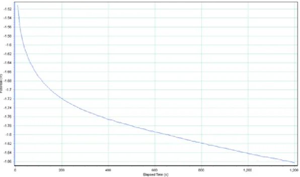
We prepare our electrodeposition setup for deposition baths by using o-ring and o-ring glass on the top of the disc in order to prevent the leakage of the gold or silver bath (Figure 3.1). The working electrode connects to the silver plate at which the desired deposition occurs by reduction of metal ions. On the other hand, the counter electrode is connected to the platinum mesh. This electrode controls the power output of the potentiostat (Versastat3) electrode (Figure 3.2). By means of sense and reference electrodes, potential difference between the counter and working electrodes is measured to keep control of the deposition rate (Figure 3.3).
We use the method of chronopotentiometry for electrodeposition, where a con-stant current pulse is driven from the counter electrode to working electrode, while the potential difference between them, is measured against as a function of time. First, we deposit silver with a current level of 1.6 mA for 1200 s from the silver bath containing 42 g/L of silver cyanide and 85 g/L of potassium cyanide (Tech-niSilver, Italgalvano to make sure that the branching portion of the membrane is totally clogged. The reduction of silver ions occurs for a potential range of 1.40 V and 1.70 V for 1.6 mA of current (Figure 3.4 and Figure 3.5). Second, we start the deposition of the first gold segment using a current level of 1.6 mA for 3600 s in the gold bath (Orotemp 24, Italgalvano). Our rate of gold deposition is 1 nm/s. The reduction of gold ions occurs for a potential range of 1.70 V and 2.65 V for 1.6 mA of current (Figure 3.6). For following Ag segment that
Figure 3.1: Our experimental setup for electrodeposition that includes template membrane disc, o-ring, and plates.
Figure 3.4: Potential trace during silver deposition into the branched part of the alumina disc.
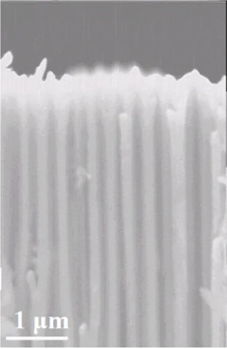
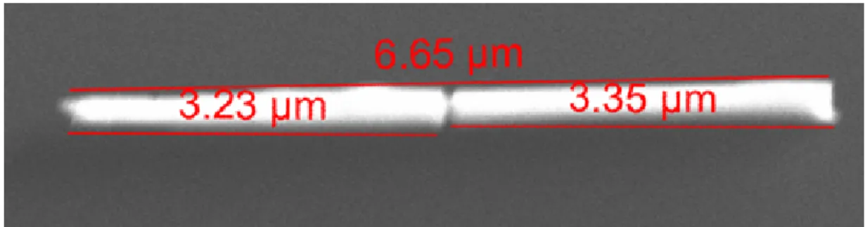
determines the size of our gap, we employ a current level of 1.6 mA while varying deposition times to make Ag segments of varying lengths tuned from 300 nm down to 20 nm. Our rate of silver deposition is 1.5 nm/s. We produced NWs with size controllable nanogaps, depending on the deposition time. Finally, we deposit Au again applying the same current and deposition time with the first Au segment (Figure 3.7). The total lengths of the Au/Ag/Au NWs can be made to extend over 20 µm (e.g., 7.78 µm and 6.65 µm as in our cases in Figure 3.8 and Figure 3.9, respectively) [46].
After finishing the electrodeposition, the backside silver layer is etched with nitric acid solution (HNO3 of 30 in concentration) and alumina disc is dissolved in
sodium hydroxide solution (NaOH of 3 M). The NWs remain in this base solution during dissolution. Subsequently, the NWs are centrifuged three times in water at 3000 r/min for 6 min for rinsing, and three times in desired solution (water or ethanol) at 3000 r/min for 6 min, and finally they get dispersed (Figure 3.10, Figure 3.11 and Figure 3.12).
Figure 3.5: Potential trace during silver deposition into the pores of the alumina disc for Ag segments of our nanowires.
Figure 3.6: Potential trace during gold deposition into the pores of the alumina disc for Au segments of our nanowires.
Figure 3.8: SEM image of an exemplary nanowire with a short Ag segment in the middle between long Au segments at the ends (with a total nanowire length of 7.78 µm).
Figure 3.9: SEM image of another nanowire with 3.23 µm and 3.35 µm long Au segments.
Figure 3.11: Backside of the membrane disc (a) before deposition and (b) after silver backing.
Figure 3.12: Silver backing is etched, membrane is dissolved and nanowires are dispersed inside solution.
Figure 3.13: Nanowire synthesized in track-etched polycarbonate membrane (a) in full view and (b) with a zoom-in across its width.
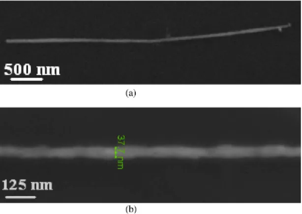
of around 40 nm, we synthesized 6 µm long Au NWs, which have diameters of 40 nm (Figure 3.13). It is very demanding to fabricate such high aspect ratio NW structures even using e-beam lithography (EBL) and focused ion beam (FIB) technology. This in-membrane NW synthesis is, on the other hand, a highly parallel and cheap process, enabling us to synthesize our NWs in massive numbers [46].
3.2
Nanogap variation study
For varying gap formation, middle Ag segments of Au/Ag/Au NWs are removed by selective chemical etching with dilute nitric acid (HNO3) solution and/or by
postbaking process at 200 ◦C for 75 min due to the oxidation of Ag. Difficulties in nanogap formation are sometimes encountered due to the high tendency of Au deposition at the walls of alumina pores, forming a meniscus at the frontline of deposition. This adversely affects the morphology of the NW tips, resulting in a curved profile across the radial axis. In addition to chemical etching, bak-ing process is also employed to remove Ag segments, and this is found to help smoothening of our nanogaps. Such thermal baking enables us to form narrower, uniform gaps, and also strengthens the electrical contacts of the gold segment ends of the NWs to the microelectrodes. Liu et al. heated the Ag segments on their own to understand its effect on NW morphology and concluded that large grains of Ag shrink in size to form smoother gaps [7]. We also characterized gap variation and showed that the length of Ag segment can be precisely controlled by the deposition time. The rate of the silver deposition is 1.5 nm/s. We syn-thesize Au-Ag-Au segmented NWs that include Ag segments with the lengths of 20-50-100-200-300 nm tuned controllably (Figure 3.14). Figure 3.15 shows dif-ferent lengths of Ag segments [46]. The length of these Ag segments is linearly proportional to the total charge injected to the pores of the membrane disc dur-ing the electrodeposition process. As we drive constant current (I), the injected charge (Q) is also linearly proportional to the deposition time (t) of silver with the simple relation of Q = I t, which conveniently allows for controlling the lengths of Ag segments. When Ag segment is selectively chemically etched, we form a
Figure 3.14: Gap length vs. charge. (Blue points represent the lengths of Ag segments, and black lines represent the standard deviation among Ag segment lengths.)
nanogap with a size equal to the size of our Ag segment. The deviation among the lengths of Ag segments stems from not being able to drive the same level of current into the pores across the entirety of the alumina disc, and this deviation increases proportionally with deposition time.
3.3
Suspended and dispersible nanostructures
It is also challenging to fabricate suspended and solution-dispersible structure by standard nanofabrication techniques such as EBL at these dimensions. EBL provides high resolution (possibly down to 10 nm) and high precision. However,
Figure 3.15: Example of Au-Ag-Au segmented nanowires with varied Ag segment lengths of 300 nm, 200 nm, 100 nm, 50 nm, and 20 nm in (a), (b), (c), (d), and (e), respectively.
EBL is a serial process where a nanostructure is patterned one at a time while in-template synthesis is massively parallel. Sioss and Keating presented a method for fabricating chains of Au and Ag nanoparticles by selective wet-etching of the alternating segments, after the wires are removed from the membrane and were coated with silicon oxide (SiO2) by surface sol-gel method [47, 48]. They
demonstrated assemblies of metal nanoparticle with desirable particle and gap sizes while those particles are kept together by SiO2layer. Similarly, Mirkin group
reported a method for fabricating arrays of nanodiscs, which is called on-wire lithography [6]. This method uniquely combines in-template electrodepostion of different compositions of nanowires and their selective wet-chemical etching to form nanodisc arrays with gaps ranging from few nanometers to several hundred nanometers. The process relies on depositing segmented nanowires consisting of two types of materials, one of which is susceptible and the other of which is resistant to etching. Followingly, these segments were blanketed by a bridging material so that the sacrificial segments can be removed while the nanodisc array is formed with previously defined disc-widths and gap-widths. Using on-wire lithography, we prepared arrays of suspended plasmonic Au nanodiscs [49]. We used a porous aluminum oxide (Al2O3) membrane as the template, with a pore
size of approximately 250 nm, and electrodeposited Au and Ni segments into the pores of the membrane at a driving current level of -1.6 mA, alternating Ni and Au baths (Orotemp Italgalvano), using a Versastat3 potentiostat. Ni segments served as the sacrificial layers, which determine the gap-widths between the Au nanodiscs after selective etching. Controlling the amount of charge passing through the pores of the membrane, we fabricated discs with size controllable disc-heights of 50 nm. After the deposition of each disc, the structure was annealed at 250◦C to form more uniform discs and gaps. Completing the deposition steps, the aluminum oxide membrane was dissolved in sodium hydroxide (NaOH) solution of 3 M, while the deposited segments remained together in the base solution during dissolution. Subsequently, they were centrifuged in water. Au and Ni segments were further immobilized on a glass slide by drop-casting and a 50 nm thick SiN dielectric film was deposited on them by plasma enhanced chemical vapour deposition (PECVD) at 250◦C, partially wrapping them as a blanket-layer. After the sonication of these glass slides, one side coated segments were detached from
the glass surface and dropped into solution. Sonication duration of 30 s was found critical not to damage structure with Au discs kept firmly inside the SiN support. The sacrificial Ni segments were finally selectively etched in 30% nitric acid (HNO3) solution, leaving behind arrays of suspended Au nanodiscs kept
Figure 3.16: Silver backing is etched, membrane is dissolved and nanowires are dispersed inside solution.
Figure 3.17: Nanowire synthesized in track-etched polycarbonate membrane (a) in full view and (b) with a zoom-in across its width.
Chapter 4
Magnetically aligned segmented
nanowires integrated with
isotropic nanocrystals
4.1
Introduction
Linear optical polarizers are passive components that selectively transmit the light with electric field parallel to the transmission axis (s-polarization) and block the transmission of the electromagnetic field in the orthogonal polarization (p-polarization). Polarizers are crucial for various optical systems and exten-sively used in applications ranging from imaging [50] and liquid crystal displays (LCDs) [51]. In the case of LCDs, an unpolarized light generated in the back-light unit is converted into polarized back-light via a polarizer. This polarization process contributes to the most significant loss in the LCDs. Thus, achieving polarized light-emitting sources are highly welcomed, which are expected to in-crease the optical efficiency of the LCDs. To date, various polarizing optical media were integrated with light-emitting materi-als to achieve polarized light sources. For example, wire-grid based polarizers [52], resonant cavities [53], plas-monic nanocavities [17], birefringent crystals [18], and liquid crystal integrated
fluorescent materials [19] can be employed to realize polarized light emission. Wire-grid polarizers have shown very good performance in terms of the de-gree of emission polarization. Zhang et al. reached a vertical (s) to parallel (p) polarization contrast of 7:1 using metallic nanogratings fabricated by elec-tron beam lithography on top of a conventional InGaN/GaN LED [20]. Ma et al. obtained an s/p polariza-tion contrast as high as 50:1, corresponding to a polarization degree of about 0.96 [21]. However, such approaches require special nanolithography techniques to achieve polarized light in the visible spectrum [52]. Sub-wavelength parallel metallic features are usually fabricated using techniques in-cluding focused ion beam lithography [54], electron beam lithography [55], and nanoimprint lithography [56], [57]. Nevertheless, these techniques are expensive, time consuming and low throughput. Alternatively, deposition of metal nanopar-ticles via layer-by-layer assembly was employed to realize polarized emission via utilizing the plasmonic nanocavity effect by Ozel et al. [17]. In these multi-layered plasmonic nanocavities polarized light emission with an s/p polarization degree of 0.80 was observed.
As an alternative approach, in this chapter, we show highly polarized light emission in coupled thin films of colloidal quantum dots (QDs) and magnetically aligned multi-segmented nanowires (NWs) [58]. These NWs consist of ferromag-netic (Ni) parts that enable alignment under externally applied magferromag-netic field. In-template synthesis of these NWs together with their magnetic field assisted alignment facilitates the fabrication of massive number of highly parallel NWs over large area thin films with low cost and fast production technique. Pre-viously, various alignment techniques have been employed including Langmuir-Blodgett [59] and external electric assisted alignment [60, 46] as well as those based on magnetic field assisted alignment [61, 62]. Among these techniques, some may require a more complex alignment setup as in the case of Langmuir-Blodgett assembly or pre-defined electrodes as in the case of electric field assisted assembly. Among these, magnetic field assisted assembly using centimeter sized commercially available magnets is a versatile tool to align NWs having ferromag-netic parts on surfaces or NWs inside a host medium without the requirement for a pre-defined electrode or surface functionalization. This makes magnetic field
assisted alignment a promising candidate for making polarizing structures. As a proof-of-concept demonstration, here we demonstrate highly polarized emission using the isotropic emitter cadmium telluride (CdTe) QDs by integrat-ing them with the aligned three-segment Au/Ni/Au NWs. The NWs were plated using template-assisted electrodeposition method [63] and aqueous CdTe QDs were synthesized colloidally as described elsewhere [64]. QDs represent an im-portant class of emitters, which are highly suitable as white-light engines for backlight of the LCDs owing to their spectrally pure color emission that can be easily matched to the color filters of LCDs to boost the optical performance. The resulting hybrid system exhibited polarized emission in visible spectrum with an s/p polarization contrast as high as 15:1 corresponding to a polarization degree of 0.88.
4.2
Results and discussion
For synthesis of aqueous CdTe colloidal QDs, 4.59 g of Cd(ClO4)26H2O was
dis-solved in 0.5 L of dionized water. Subsequently, 1.33 g of thioglycolic acid (TGA) was added to the solution and the pH of the mixture was set to 12.0 by addition of NaOH. Later, 0.8 g of Al2Te3 was deaerated under Ar flow for approximately
60 min. Following the addition of 0.5 M H2SO4 onto Al2Te3 to produce H2Te gas,
the solution was heated until boiling point, at which temperature the nanocrystal quantum dots start to form. The reaction was continued about 20 h, at the end of which the QDs exhibited an emission peak at 625 nm. The absorption (black line) and emission spectra (red line) of the synthesized CdTe quantum dots are given in Figure 4.1.
Using the Whatman Anodisc membrane (with a pore density of 109 cm-2) as
our template, three-segment Au/Ni/Au NWs having diameters of ca. 250 nm were plated by employing electrodeposition method. Prior to the plating, a 200 nm thick silver layer serving as the working electrode was thermally evaporated on the backside of the membrane. As the counter electrode mesh platinum was
Figure 4.1: Absorption (black line) and emission spectra (red line) of the synthe-sized CdTe QDs emitting around 625 nm.
used and placed 5 cm above the membrane inside an O-ring glass tube. The process started with the electrodeposition of 2 µm thick silver using the silver bath (TechniSilver E-2, Italgalvano, 11.5 % potassium silver cyanide) to clog the branching portion of the membrane. For gold segments, we used Orotemp 24 (6.87 % potassium aurocyanide) and drove -1.6 mA by Versastat 3 potentiostat to deposit approximately 1.5 µm long Au segments. After rinsing, we drove -1.6 mA again to deposit nickel using the nickel bath, which is composed of nickel sulfamate (20-35 %), nickel bromide (0.5-1.5 %), and boric acid (1-3 %), to obtain 7 µm long nickel segments. The final gold segments of 1.5 µm in length were plated as in the first step following the rinsing. At these current levels, the average deposition rates of gold and nickel were 2 nm/s and 1.5 nm/s, respectively. Gold segments constituted of ca. 3 µm and the remaining 7 µm of the NWs was nickel (Figure 4.2). After deposition, the silver back-coating was etched with a nitric acid solution (HNO3 of 30 %) and the alumina disc was dissolved in a sodium
hydroxide solution (NaOH of 3M). The synthesized NWs remained in the base solution. Finally, the NWs were centrifuged three times in DI water at 3000 rpm and stored in DI water.
Figure 4.2: (a) Arrays of Au/Ni/Au segmented NWs inside the alumina mem-brane and (b) the NWs immobilized on glass after etching of the memmem-brane.
An externally applied magnetic field enables magnetization of these NWs and helps to rotate and position them along the direction of the applied field. This is mainly due to their high aspect ratio geometry, which allows the Ni parts of the NWs to experience higher magnetization and induce magnetic charges to interact with the external magnetic field. As a result, a torque is exerted on the NWs causing them to align in the direction of the field. The induced magnetic moment (L) can be expressed using the relation L=mlHsinΘ, where m, l, H, and Θ denote the induced dipole strength, the ferromagnetic segment length, the external magnetic field, and the angle between the magnetic field and the longitudinal axis of the NW, respectively 17. Longer the ferromagnetic segment length (l) of the NWs and/or higher the external magnetic field (H), we observe a higher torque induced on the wires, thus leading to a better alignment. The aligned metal NWs constructed a grid-like architecture in which they act as a good reflector for one polarization while they transmit a higher portion of the electromagnetic field with the perpendicular polarization.
To investigate the potential of the assemblies of these segmented NWs to achieve polarized light from the QDs, we numerically investigated the hybrid ar-chitecture comprising of aligned metal NWs and CdTe QDs using finite difference time domain (FDTD) technique (Figure 4.2). Single segment NWs comprising of 10 µm long Ni were used in the simulations in addition to Au-Ni-Au three segment NWs having 1.5 µm long Au segments and 7 µm long Ni segment to understand the effects of Au segments in the polarizing effect of the obtained emission. The QD layer is modeled using the real and imaginary parts of the refractive index as measured by optical ellipsometry. In the FDTD simulations, light emitted by the QD film is assumed to pass through the aligned NW networks, each of which contain randomly positioned NWs having an average NW-to-NW separation of 250, 300, 350, and 400 nm. This randomly distributed NW matrix is along the lateral plane to account for the very large area of the sample that can be up to a few cm2 in size. We separately investigated the parallel and perpendicular
polarization that is emitted by the QDs and monitored the transmitted power for these two orthogonal polarizations.
Figure 4.3: A representative image illustrating FDTD simulation structure. (b) Numerical simulation results indicating the ratio of s- and p-polarizations trans-mitted through Au/Ni/Au and Ni NWs at the emission peak of QDs (650 nm). (c) Normalized transmitted intensities through Au/Ni/Au and Ni NWs at the emission peaks of QDs for s- and p-polarizations.
the emitted light experiences a conductive medium and is absorbed/scattered. On the other hand, perpendicular polarized electric field components of the emitted light interact much less with the aligned NWs; thus, perpendicular polarized light is transmitted more. The results of the simulations are presented in Figures 4.3 (b) and 4.3 (c). According to these results, aligned Au/Ni/Au and Ni NWs exhibit anisotropic character (i.e., increasing s/p polarization contrast for the transmission) that is enhanced as the inter-NW distance is decreased. In the case of Au/Ni/Au NWs, polarization contrast larger than 10:1 is possible to achieve with inter-NW distance that is smaller than 250 nm. In the case of Ni NWs, a higher polarization contrast could be achieved at the expense of reduced transmitted power since Ni introduces extra loss due to their optical absorption. For the magnetic alignment, two neodium magnets, each of 5 mm by 10 mm by 40 mm in size and generating a magnetic field of 400 Gauss, were used to align the NWs. For a proof-of-concept demonstration, Au/Ni/Au NWs were used instead of Ni NWs, which tend to break during the etching process of the silver from the back of the membranes. In addition, post thermal baking process strengthens the Au/Ni interface to keep segmented NWs robust and undamaged. To avoid quenching of the emission from the QDs and obtain an appropriate level of viscosity so that the NWs were not pulled to the sides of the film while drying, poly(vinyl pyrolidone) (PVP) was used as a host material. We prepared two different films comprising of the same amount of QDs but having different amounts of NWs. 500 µL of the multi-segmented NW in water was mixed with 750 µL of PVP, and 1600 µL CdTe QD solution was mixed with 1200 µL of PVP. The NW:PVP solutions (375 µL and 500 µL) were drop-casted on a glass substrate and left for drying overnight under magnetic field. Since PVP provides a reasonable level of viscosity, it allows for controlling the positioning of NWs as it is required for a higher polarization contrast. Furthermore, once it dries, PVP is a strong host material to keep the NWs in the orientation that they were aligned and provide a three dimensional structure where the NWs are highly aligned along one dimension. Subsequent to the deposition of the NWs, QD:PVP solution (700 µL) was drop-casted over the NW films and again the system was left for drying overnight. The hybrid film architecture and the alignment setup
Figure 4.4: (a) Alignment during hybridization of the CdTe QDs with aligned ferromagnetic NWs in PVP host film between two Neodium magnets. Microscopy images of (b) uniformly distributed NWs and (c) dense and uniformly distributed NWs.
are illustrated in Figure 4.4 (a).
As the optical microscopy images show, the NWs were clearly aligned in the direction of the magnetic field and form a one dimensional array. The uniform alignment regions, where the NWs tend to form regular grid like structures are shown in Figures 4.4 (b) and 4.4 (c). Due to the random nature of the alignment process, non-uniformities cannot be completely avoided, which would limit the extinction ratio (i.e., the ratio of the s-polarized light to p-polarized light). How-ever, still reasonably large values were obtained depending on the amount of the NWs as explained in the characterization section.
Figure 4.5: Illustration of the characterization setup for the polarization degree of the QD integrated aligned NW films.
Our optical characterization setup is illustrated in Figure 4.4. These QD inte-grated NW hybrid films were excited using a laser diode emitting at 375 nm. The emitted light by the QDs was collected through a linear polarizer, a monochroma-tor and a photomultiplier tube. The emission intensity of the QDs was recorded as the polarizer is rotated to measure the perpendicular and parallel polariza-tion components of the light emitted by the QDs that is transmitted through the NWs.
When bare CdTe QDs were employed, which were not integrated to the NWs, unpolarized light is emanated at a peak emission wavelength of 650 nm in solid film. The s/p polarization contrast is close to 1:1 when the QDs are decorated on top of two different NW films having different film thicknesses (375 and 500 µL of NW:PVP). The emission intensities of the QDs collected by the detector after the polarizer in s- and p-polarizations at the receiver end are presented in Figure 4.6 for the thin and thick NW matrices. The blue curves in Figure 4.6 show the s/p polarization contrast as a function of the wavelength. Our results reveal that aligned NWs in PVP matrix substantially polarizes the emission of the QDs. For the thin NW:PVP sample, the s/p polarization contrast reaches 10:1, while it gets at 15:1 for the thicker NW:PVP sample. We attribute this to the increased number of aligned NWs that enhance the polarization contrast. We
Figure 4.6: Photoluminescence spectra intensity of the QDs integrated on the NW:PVP samples in s- and p- polarizations (red and black lines) along with the s/p contrast (blue line) from (a) the thinner and (b) the thicker NW:PVP films. The maximum contrast of the s/p polarizations was found to be 10:1 for the thinner film and 15:1 for the thicker one.
further observe that the contrast of the optical polarizations has a slowly varying trend with respect to the wavelength. We attribute such a large bandwidth of the polarization contrast due to the random nature of the hybrid films, where the distribution of aligned NWs is not perfectly uniform within the film.
4.3
Conclusion
In summary, we proposed and demonstrated a proof-of-concept hybrid thin film system for the generation of polarized light with a contrast of polarizations per-pendicular to parallel larger than 15:1 in the visible range by employing multi-segmented NWs having ferromagnetic parts, which are well aligned under external magnetic field. The proposed approach makes use of a much cheaper and easier fabrication procedure compared to the conventional expensive fabrication tech-niques. Furthermore, we verified the experimental results of highly polarized light generation by FDTD simulations, which revealed the relation between inter-NW distance and the achieved polarization contrast.
Chapter 5
Arrays of suspended plasmonic
nanodiscs
5.1
Introduction
Plasmonic structures enable enhanced light utilization for optoelectronic devices owing to their unique, strong and tunable electric field localization leading to increased scattering and absorption properties [1, 2, 3]. Various nanopatterned plasmonic structures have been proposed to date, which typically use the nanofab-rication method of electron beam lithography (EBL) or nanoimprint lithogra-phy [4, 5]. Although these techniques offer high resolution and allow for a more deterministic nanostructure layout for plasmonics, these technologies are quite costly and limited in high throughput. Alternatively, solution processed nanos-tructures have emerged, for example, metallic nanodiscs, which are synthesized using in-template electrodeposition [46, 65], followed by simple selective etching of sacrificial metal layers. These nanodiscs are promising for nanoplasmonics be-cause their optical properties may be fine-tuned either via the disc-gap or the disc-width [13, 12, 66]. The spectral line shape of the localized surface plasmon (LSP) resonance of a metallic nanoparticle, as obtained when measuring absorp-tion, or scattering cross sections as a function of photon energy, depends on the
material and particle size. These absorption and scattering mechanisms deter-mine the local field enhancement around the plasmonic nanoparticles, which are important issues in sensing [67], surface enhanced Raman spectroscopy (SERS) [8] and plasmon enhanced fluorescence [11].
In this chapter, we demonstrate lateral arrays of Au nanodiscs with controlled disc-gap and disc-width, which can range from 20 nm to several hundred nanome-ters using the in-template synthesis to allow for the tailoring of the scattering properties [49]. This has resulted in massive numbers of easily and inexpensively fabricated arrays of nanodisc structures. The achievable resolution of our fabri-cation approach reaches down to approximately 20 nm. Fabricating such three-dimensional suspended and liquid dispersible architectures is not easily possible by other techniques such as EBL. Here, we report the plasmonic properties of these suspended nanodisc structures including the polarization-dependent scat-tering spectra as a function of disc-gap/-width parameters computed numerically and measured experimentally.
5.2
Results and discussion
We study the polarization dependent absorption and scattering properties of the nanodisc arrays presented in Figure 5.1. We model our discs to tailor the light spectra scattered from these Au discs with varying disc-widths (w) for different disc-gaps (g) (Figure 5.2 (a)). Under unpolarized illumination incident on discs, we observe different scattering spectra with respect to the position of the polarizer with respect to nanodiscs. Figures 5.2 (b) and (c) present the computed quality scattering factors of the nanodisc array for polarization normal and parallel to the discs by finite-difference time-domain (FDTD) simulations. Here the disc diameter (D) is 250 nm, which is the membrane pore size of our template used during electrodeposition.
For polarization normal to the discs, we observe strong plasmonic coupling de-pending on the gap size (g) between the discs. The electric field localized between
Figure 5.1: (a) Illustration of the suspended plasmonic nanodisc array fabrication using in-template synthesis. (b) SEM images of the suspended gold nanodisc array fabrication steps from in-template synthesis of segmented nanowires to selective etching of Ni segments leaving behind arrays of suspended gold nanodiscs inside SiN dielectric-wrap.
Figure 5.2: (a) A representative image indicating FDTD simulation structure. Scattering quality factor under unpolarized illumination: (b) Strong plasmonic coupling (at shorter wavelengths) depending on the gap-width (g) for polarization normal to nanodiscs. (c) Weak coupling (at longer wavelengths) between the discs for polarization parallel to the discs for varying disc-width (w).
Figure 5.3: Absorption quality factor of the nanodiscs vs. their gap-width. Strong plasmonic coupling is observed at longer wavelengths depending on the gap-width. the discs is found to increase with this coupling. We observe a scattering peak at shorter wavelengths in Figure 5.2 (b) with a disc width (w) of approximately 50 nm and above. However, in the case when the polarization is horizontal to discs, we do not observe strong coupling between the discs in that direction. With 250 nm disc diameter (D), we observe scattering at longer wavelengths in Figure 5.2 (c).
Absorption and scattering quality factor of the nanodiscs vs. their gap-width. Strong plasmonic coupling is observed at longer wavelengths depending on the gap-width (Figures 5.3, 5.4 and 5.5).
For the in-template synthesis of the gold nanodisc array, we used a porous aluminum oxide (Al2O3) membrane as the template, with a pore size of
approx-imately 250 nm, and electrodeposited Au and Ni segments into the pores of the membrane at a driving current level of -1.6 mA, alternating Ni and Au baths
Figure 5.4: Scattering quality factor of the nanodiscs vs. their gap-width. Strong plasmonic coupling is observed at longer wavelengths depending on the gap-width.
Figure 5.5: Localized electric field outside the nanodiscs vs. their gap-width. Strong plasmonic coupling is observed at longer wavelengths depending on the gap-width.