VCU Scholars Compass
Electrical and Computer Engineering Publications
Dept. of Electrical and Computer Engineering
2005
A comprehensive review of ZnO materials and
devices
Ü. Özgür
Virginia Commonwealth University, [email protected]
Ya. I. Alivov
Virginia Commonwealth University
C. Liu
Virginia Commonwealth University
See next page for additional authors
Follow this and additional works at:
http://scholarscompass.vcu.edu/egre_pubs
Part of the
Electrical and Computer Engineering Commons
Ozgur, U., Alivov, Y. I., Liu, C., et al. A comprehensive review of ZnO materials and devices. Journal of Applied Physics 98, 041301 (2005). Copyright © 2005 AIP Publishing LLC.
This Article is brought to you for free and open access by the Dept. of Electrical and Computer Engineering at VCU Scholars Compass. It has been accepted for inclusion in Electrical and Computer Engineering Publications by an authorized administrator of VCU Scholars Compass. For more information, please [email protected].
Downloaded from
Ü. Özgür, Ya. I. Alivov, C. Liu, A. Teke, M. A. Reshchikov, S. Doğan, Vitaliy Avrutin, S.-J. Cho, and H. Morkoç
APPLIED PHYSICS REVIEWS
A comprehensive review of ZnO materials and devices
Ü. Özgür,a兲 Ya. I. Alivov, C. Liu, A. Teke,b兲 M. A. Reshchikov, S. Doğan,c兲 V. Avrutin, S.-J. Cho, and H. Morkoçd兲
Department of Electrical Engineering and Physics Department, Virginia Commonwealth University, Richmond, Virginia 23284-3072
共Received 2 February 2005; accepted 13 June 2005; published online 30 August 2005兲
The semiconductor ZnO has gained substantial interest in the research community in part because of its large exciton binding energy共60 meV兲 which could lead to lasing action based on exciton recombination even above room temperature. Even though research focusing on ZnO goes back many decades, the renewed interest is fueled by availability of high-quality substrates and reports of p-type conduction and ferromagnetic behavior when doped with transitions metals, both of which remain controversial. It is this renewed interest in ZnO which forms the basis of this review. As mentioned already, ZnO is not new to the semiconductor field, with studies of its lattice parameter dating back to 1935 by Bunn关Proc. Phys. Soc. London 47, 836 共1935兲兴, studies of its vibrational properties with Raman scattering in 1966 by Damen et al.关Phys. Rev. 142, 570 共1966兲兴, detailed optical studies in 1954 by Mollwo 关Z. Angew. Phys. 6, 257 共1954兲兴, and its growth by chemical-vapor transport in 1970 by Galli and Coker关Appl. Phys. Lett. 16, 439 共1970兲兴. In terms of devices, Au Schottky barriers in 1965 by Mead关Phys. Lett. 18, 218 共1965兲兴, demonstration of light-emitting diodes共1967兲 by Drapak 关Semiconductors 2, 624 共1968兲兴, in which Cu2O was used as the p-type material, metal-insulator-semiconductor structures共1974兲 by Minami et al. 关Jpn. J. Appl. Phys. 13, 1475共1974兲兴, ZnO/ZnSe n-p junctions 共1975兲 by Tsurkan et al. 关Semiconductors
6, 1183 共1975兲兴, and Al/Au Ohmic contacts by Brillson 关J. Vac. Sci. Technol. 15, 1378 共1978兲兴
were attained. The main obstacle to the development of ZnO has been the lack of reproducible and low-resistivity p-type ZnO, as recently discussed by Look and Claflin关Phys. Status Solidi B 241, 624 共2004兲兴. While ZnO already has many industrial applications owing to its piezoelectric properties and band gap in the near ultraviolet, its applications to optoelectronic devices has not yet materialized due chiefly to the lack of p-type epitaxial layers. Very high quality what used to be called whiskers and platelets, the nomenclature for which gave way to nanostructures of late, have been prepared early on and used to deduce much of the principal properties of this material, particularly in terms of optical processes. The suggestion of attainment of p-type conductivity in the last few years has rekindled the long-time, albeit dormant, fervor of exploiting this material for optoelectronic applications. The attraction can simply be attributed to the large exciton binding energy of 60 meV of ZnO potentially paving the way for efficient room-temperature exciton-based emitters, and sharp transitions facilitating very low threshold semiconductor lasers. The field is also fueled by theoretical predictions and perhaps experimental confirmation of ferromagnetism at room temperature for potential spintronics applications. This review gives an in-depth discussion of the mechanical, chemical, electrical, and optical properties of ZnO in addition to the technological issues such as growth, defects, p-type doping, band-gap engineering, devices, and nanostructures. © 2005 American Institute of Physics.关DOI: 10.1063/1.1992666兴
TABLE OF CONTENTS
I. INTRODUCTION. . . 2
II. PROPERTIES OF ZnO. . . 3
A. Crystal structures. . . 3
B. Lattice parameters. . . 6
C. Electronic band structure. . . 7
D. Mechanical properties. . . 12 E. Lattice dynamics. . . 15 F. Thermal properties. . . 18 1. Thermal-expansion coefficients. . . 18 2. Thermal conductivity. . . 19 3. Specific heat. . . 21
G. Electrical properties of undoped ZnO. . . 22
1. Low-field transport. . . 23
a兲Electronic mail: [email protected]
b兲Present address: Balikesir University, Faculty of Art and Science, Depart-ment of Physics, 10100 Balikesir, Turkey.
c兲Present address: Atatürk University, Faculty of Art and Science, Depart-ment of Physics, 25240 Erzurum, Turkey.
d兲Electronic mail: [email protected]
0021-8979/2005/98共4兲/041301/103/$22.50 98, 041301-1 © 2005 American Institute of Physics
2. High-field transport. . . 25
III. ZnO GROWTH. . . 26
A. Bulk growth. . . 26 B. Substrates. . . 28 C. rf magnetron sputtering. . . 29 D. Molecular-beam epitaxy. . . 30 E. Pulsed-laser deposition. . . 34 F. Chemical-vapor deposition. . . 36
IV. OPTICAL PROPERTIES OF ZnO. . . 39
A. Prelude. . . 39
B. Optical transitions in ZnO. . . 39
1. Free excitons and polaritons. . . 39
2. Bound excitons. . . 42
3. Two-electron satellites in PL. . . 44
4. DAP and LO-phonon replicas in PL. . . 45
5. Temperature-dependent PL measurements.. 45
C. Time-resolved PL on ZnO. . . 47
D. Refractive index of ZnO. . . 48
E. Stimulated emission in ZnO. . . 51
1. Thin films. . . 51
2. Polycrystalline ZnO films and “random lasers”. . . 54
3. Multiple-quantum wells. . . 56
4. Stimulated-emission dynamics. . . 56
V. DEFECTS IN ZnO. . . 57
A. Predictions from first principles. . . 57
B. Experimental studies of native and unintentionally introduced defects. . . 58
1. Shallow acceptor in ZnO. . . 58
2. Green luminescence band. . . 59
3. Yellow luminescence band. . . 61
4. Red luminescence band. . . 62
VI. DOPING OF ZnO. . . 62
A. n-type doping. . . . 62
B. p-type doping. . . . 63
1. Nitrogen doping. . . 63
2. Codoping method: Nitrogen+ group III. . . 65
3. Other dopants in group V. . . 67
VII. ZnO-BASED DILUTE MAGNETIC SEMICONDUCTORS. . . 68
A. Theory of ZnO-based magnetic semiconductors. . . 69
B. Experimental results on ZnO-based magnetic semiconductors. . . 72
VIII. BAND-GAP ENGINEERING. . . 76
A. MgxZn1−xO alloy. . . 77
B. CdyZn1−yO alloy. . . 78
IX. PROCESSING, DEVICES, AND HETEROSTRUCTURES. . . 79
A. Ohmic contacts to ZnO. . . 79
B. Schottky contacts to ZnO. . . 80
C. Heterostructure devices. . . 82
1. Light-emitting devices. . . 83
2. Photodiodes. . . 85
D. Metal-insulator-semiconductor diodes. . . 86
E. Transparent thin-film transistors. . . 87
X. ZnO NANOSTRUCTURES. . . 88
XI. SUMMARY. . . 95
I. INTRODUCTION
There has been a great deal of interest in zinc oxide 共ZnO兲 semiconductor materials lately, as seen from a surge of a relevant number of publications. The interest in ZnO is fueled and fanned by its prospects in optoelectronics appli-cations owing to its direct wide band gap 共Eg⬃3.3 eV at
300 K兲. Some optoelectronic applications of ZnO overlap with that of GaN, another wide-gap semiconductor 共Eg
⬃3.4 eV at 300 K兲 which is widely used for production of green, blue-ultraviolet, and white light-emitting devices. However, ZnO has some advantages over GaN among which are the availability of fairly high-quality ZnO bulk single crystals and a large exciton binding energy共⬃60 meV兲. ZnO also has much simpler crystal-growth technology, resulting in a potentially lower cost for ZnO-based devices.
As indicated in the abstract, ZnO is not really a newly discovered material. Research on ZnO has continued for many decades with interest following a roller-coaster pattern. Interest in this material at the time of this writing is again at a high point. In terms of its characterization, reports go back to 1935 or even earlier. For example, lattice parameters of ZnO were investigated for many decades.1–9Similarly, opti-cal properties and processes in ZnO as well as its refractive index were extensively studied many decades ago.10–25 Vi-brational properties by techniques such as Raman scattering were also determined early on.26–32 Investigations of ZnO properties presumes that ZnO samples were available. Growth methods not much different from what is employed lately have been explored, among which are chemical-vapor transport,33 vapor-phase growth,34 hydrothermal growth35 which also had the additional motivation of doping with Li in an effort to obtain p-type material, high-quality platelets,36 and so on.37
The ZnO bulk crystals have been grown by a number of methods, as has been reviewed recently,38 and large-size ZnO substrates are available.39–41 High-quality ZnO films can be grown at relatively low temperatures 共less than 700 ° C兲. The large exciton binding energy of ⬃60 meV paves the way for an intense near-band-edge excitonic emis-sion at room and higher temperatures, because this value is 2.4 times that of the room-temperature 共RT兲 thermal energy 共kBT = 25 meV兲. There have also been a number of reports on
laser emission from ZnO-based structures at RT and beyond. It should be noted that besides the above-mentioned proper-ties of ZnO, there are additional properproper-ties which make it preferable over other wide-band-gap materials: its high-energy radiation stability and amenability to wet chemical etching.38 Several experiments confirmed that ZnO is very resistive to high-energy radiation,42–44making it a very suit-able candidate for space applications. ZnO is easily etched in all acids and alkalis, and this provides an opportunity for fabrication of small-size devices. In addition, ZnO has the same crystal structure and close lattice parameters to that of GaN and as a result can be used as a substrate for epitaxial growth of high-quality GaN films.45,46
ZnO has recently found other niche applications as well, such as fabrication of transparent thin-film transistors, where the protective covering preventing light exposure is
nated since ZnO-based transistors are insensitive to visible light. Also up to 2⫻1021 cm−3 charge carriers can be intro-duced by heavy substitutional doping into ZnO. By control-ling the doping level electrical properties can be changed from insulator through n-type semiconductor to metal while maintaining optical transparency that makes it useful for transparent electrodes in flat-panel displays and solar cells. ZnO is also a promising candidate for spintronics applica-tions. Dietl et al.47predicted a Curie temperature of⬎300 K for Mn-doped ZnO. n-type doping in Fe-, Co-, or Ni-alloyed ZnO was predicted to stabilize high-Curie-temperature ferro-magnetism. There have been a number of publications which appear to confirm these predictions, as has been reviewed recently,48,49albeit with a good deal of controversy, as will be discussed in Sec. VII.
However, one important problem should be overcome before ZnO could potentially make inroads into the world of optoelectronics devices: the growth of p-type-conductivity ZnO crystals. Despite all the progress that has been made and the reports of p-type conductivity in ZnO films using various growth methods and various group-V dopant ele-ments共N, P, As, and Sb兲, a reliable and reproducible high-quality p-type conductivity has not yet been achieved for ZnO. Therefore, it remains to be the most pivotal topic in ZnO research today, and congruently most of the research efforts are directed just to solving this problem. In order to overcome this bottleneck and to control the material’s prop-erties, a clear understanding of physical processes in ZnO is necessary in addition to obtaining low n-type background. In spite of many decades of investigations, some of the basic properties of ZnO still remain unclear. For example, the na-ture of the residual n-type conductivity in undoped ZnO films, whether being due to impurities of some native defect or defects, is still under some degree of debate. Some authors ascribe the residual background to intrinsic defects关oxygen vacancies 共VO兲 and interstitial zinc atoms 共Zni兲兴, and others
to noncontrollable hydrogen impurities introduced during growth. The well-known green band in ZnO luminescence spectra 共manifesting itself as a broad peak around 500– 530 nm兲, observed nearly in all samples regardless of growth conditions, is related to singly ionized oxygen vacan-cies by some and to residual copper impurities by others. Simply, a requisite consensus is lacking.
While p-type ZnO is difficult to attain, the advantages of ZnO are being explored and exploited by alternative methods such as heteroepitaxy in which p-n heterostructures can be obtained by depositing n-type ZnO films on other p-type materials while still utilizing ZnO as the active layer. Progress has been made in this arena with a number of het-erostructures fabricated wherein one of the following, Si, NiO, GaN, AlGaN, SiC, ZnTe, CuO, CdTe, etc., plays the role of p-type layer. In particular, high-intensity UV emission has been observed from the n-ZnO / p-AlGaN heterojunction in which ZnO served as the active layer. These results are just harbingers of what can be expected of ZnO in an effort to position it for future device applications. As in the early developments of GaN predating the demonstration of p-type
conductivity, metal-insulator-semiconductor device struc-tures not requiring p-type ZnO have been introduced but lack the high efficiency.
In this paper we collate the properties of ZnO as well as review the recent progress in ZnO research. This present review is distinguishable from the other reviews50–55in that the previous ones focused mainly on material processing, doping, and transport properties, while the present one treats those topics in greater depth in addition to an in-depth dis-cussion of the growth, optical properties, p-type doping, and device fabrication aspects. The organization of this review is as follows: First, structural, chemical, and electrical proper-ties of undoped ZnO are discussed in Sec. II. This is fol-lowed by ZnO crystal growth, both bulk and film共Sec. III兲, and optical properties of ZnO共Sec. IV兲. Sections V–VII are devoted, respectively, to defects in ZnO, doping, and mag-netic properties. Alloys of ZnO 共band-gap engineering兲 are discussed in Sec. VIII, and this is followed by ZnO-based devices and their applications 共Sec. IX兲. Finally, ZnO nano-structures are reviewed in Sec. X.
II. PROPERTIES OF ZnO
In this section crystal structures, inclusive of lattice pa-rameters, electronic band structures, mechanical properties, inclusive of elastic contants and piezoelectric constants, lat-tice dynamics and vibrational processes, thermal properties, electrical properties, and low-field and high-field carrier transports are treated.
A. Crystal structures
Most of the group-II-VI binary compound semiconduc-tors crystallize in either cubic zinc-blende or hexagonal wurtzite structure where each anion is surrounded by four cations at the corners of a tetrahedron, and vice versa. This tetrahedral coordination is typical of sp3 covalent bonding, but these materials also have a substantial ionic character. ZnO is a II-VI compound semiconductor whose ionicity re-sides at the borderline between covalent and ionic semicon-ductor. The crystal structures shared by ZnO are wurtzite 共B4兲, zinc blende 共B3兲, and rocksalt 共B1兲, as schematically shown in Fig. 1. At ambient conditions, the thermodynami-cally stable phase is wurtzite. The zinc-blende ZnO structure can be stabilized only by growth on cubic substrates, and the rocksalt 共NaCl兲 structure may be obtained at relatively high pressures.
The ground-state total energy of ZnO in wurtzite, zinc-blende, and rocksalt structures has been calculated as a func-tion of unit-cell volume using a first-principles periodic Hartree-Fock 共HF兲 linear combination of atomic orbitals 共LCAO兲 theory by Jaffee and Hess.56
The total-energy data versus volume for the three phases are shown in Fig. 2 along with the fits to the empirical functional form of the third-order Murnaghan equation, which is used to calculate the derived structural properties,
E共V兲 = E0− B0V0 B
⬘
− 1+ B0V B⬘
冋
共V0/V兲 B⬘ B⬘
− 1 + 1册
, 共1兲where E0, V0, and B0 are the total energy, volume per ZnO f.u., and bulk modulus at zero pressure共P兲, respectively, and B
⬘
= dB / dP is assumed to be constant.In this calculation, although E0represents the sum of the total energies of isolated neutral Zn and O atoms, the abso-lute value of the energy at the minimum of each curve was considered as a rough estimate of the equilibrium cohesive energy of the corresponding ZnO phases. The total energy 共or roughly the cohesive energy per bond兲 in wurtzite variety was calculated to be −5.658 eV for wurtzite, −5.606 eV for zinc-blende, and −5.416 eV for rocksalt phases. Later, Jaffe et al.57 employed the density-functional theory共DFT兲 using two different approximations, namely, the local-density ap-proximation共LDA兲 and the generalized gradient approxima-tion共GGA兲, in the exchange-correlation function to calculate the total energy and electronic structure of ZnO. In these calculations, cohesive energies were obtained by subtracting the total energy per ZnO f.u. of the solid at its equilibrium lattice constant from the energy of the corresponding isolated atoms. Using the LDA calculation technique, the equilibrium cohesive energy of ZnO was reported as −9.769, −9.754, and −9.611 eV for wurtzite, zinc-blende, and rocksalt structures, respectively. The best agreement with the experimental value of −7.52 eV, which is deduced from experimental Zn heat of
vaporization, ZnO enthalpy of formation, and O2 binding energy for the wurtzite phase,58was achieved using the GGA technique. It gives −7.692, −7.679, and −7.455 eV cohesive energies for wurtzite, zinc-blende, and rocksalt phases, re-spectively. In these two techniques, although the calculated energy difference ⌬EW-ZB between the wurtzite and zinc-blende lattices is small 共about −15 and −13 meV/atom for LDA and GGA, respectively兲, whereas it is relatively large, ⬃50 meV/atom, for Hartree-Fock approximation, the wurtz-ite form is energetically preferable compared to zinc blende and rocksalt.
The wurtzite structure has a hexagonal unit cell with two lattice parameters, a and c, in the ratio of c / a =
冑
8 / 3 = 1.633 and belongs to the space group of C64 or P63mc. A schematic representation of the wurtzitic ZnO structure is shown in Fig. 3. The structure is composed of two interpen-etrating hexagonal-close-packed 共hcp兲 sublattices, each of which consists of one type of atom displaced with respect to each other along the threefold c-axis by the amount of u = 3 / 8 = 0.375共in an ideal wurtzite structure兲 in fractional co-ordinates 共the u parameter is defined as the length of the bond parallel to the c axis, in units of c兲. Each sublattice includes four atoms per unit cell and every atom of one kind 共group-II atom兲 is surrounded by four atoms of the other kind共group VI兲, or vice versa, which are coordinated at the edges of a tetrahedron. In a real ZnO crystal, the wurtzite structure deviates from the ideal arrangement, by changing the c / a ratio or the u value. It should be pointed out that a strong correlation exists between the c / a ratio and the u parameter in that when the c / a ratio decreases, the u param-eter increases in such a way that those four tetrahedral dis-tances remain nearly constant through a distortion of tetrahe-dral angles due to long-range polar interactions. These two slightly different bond lengths will be equal if the following relation holds: u =冉
1 3冊冉
a2 c2冊
+ 1 4. 共2兲Since the c / a ratio also correlates with the difference of the electronegativities of the two constituents, components with
FIG. 1. Stick and ball representation of ZnO crystal structures:共a兲 cubic rocksalt共B1兲, 共b兲 cubic zinc blende 共B3兲, and 共c兲 hexagonal wurtzite 共B4兲. The shaded gray and black spheres denote Zn and O atoms, respectively.
FIG. 2. Total energy vs volume共both per ZnO f.u.兲 for the three phases: zinc blende共squares兲, wurtzite 共diamonds兲, and rocksalt 共circles兲. The zero of energy is the sum of the total energy of an isolated Zn and an isolated O atom.关Reprinted with permission from J. E. Jaffe and A. C. Hess, Phys. Rev. B 48, 7903共1993兲. Copyright 1993 by the American Physical Society.兴
FIG. 3. Schematic representation of a wurtzitic ZnO structure having lattice constants a in the basal plane and c in the basal direction; u parameter is expressed as the bond length or the nearest-neighbor distance b divided by c 共0.375 in ideal crystal兲, and␣and共109.47° in ideal crystal兲 are the bond angles.
the greatest differences show the largest departure from the ideal c / a ratio.59
Like other II-VI semiconductors, wurtzite ZnO can be transformed to the rocksalt 共NaCl兲 structure at relatively modest external hydrostatic pressures. The reason for this is that the reduction of the lattice dimensions causes the interi-onic Coulomb interaction to favor the iinteri-onicity more over the covalent nature. The space-group symmetry of the rocksalt-type of structure is Fm3m, and the structure is sixfold coor-dinated. However, the rocksalt structure cannot be stabilized by the epitaxial growth. In ZnO, the pressure-induced phase transition from the wurtzite 共B4兲 to the rocksalt 共B1兲 phase occurs at approximately 10 GPa and a large volume decrease of about 17%, as reported by Bates et al.60They found that high-pressure cubic phase is metastable for long periods of time even at ambient pressure and above 100 ° C. More re-cently, energy-dispersive x-ray diffraction 共EDXD兲 using synchrotron radiation has been employed to probe the phase transition in ZnO.61,62 Gerward and Olsen61 and Recio et al.62 observed that the hexagonal wurtzite structure of ZnO undergoes a structural phase transformation with a transition pressure ptr= 10 GPa and completed at about 15 GPa. The measured lattice-plane spacings as a function of pressure for the B1 phase are shown in Fig. 4. Accordingly, a large frac-tion of the B1 phase is retained when the pressure is released, indicating the metastable state of the rocksalt phase of ZnO even at zero pressure.
In contrast, using in situ x-ray diffraction, Jamieson63 and later, using EDXD, Desgreniers64reported that this tran-sition is reversible at room temperature. A large number of EDXD spectra were recorded at pressures ranging from
0.1 MPa to 56± 1 GPa at room temperature with increasing and decreasing pressures. A clear wurtzite-to-rocksalt transi-tion was observed starting at 9.1± 0.2 GPa with increasing pressure. The two phases coexist over a pressure range of 9.1– 9.6 GPa, as shown in Fig. 5. The structural transition is completed at 9.6 GPa, resulting in a 16.7% change in the unit-cell volume. Upon decompression, it was observed that ZnO reverts to the wurtzite structure at 1.9± 0.2 GPa, below which a single phase is present. The phase hysteresis is con-sequently substantial. Similar hysteresis was also reported by Karzel et al.65 for this transition from x-ray and Zn-Mössbauer spectroscopy studies. The transition pressure was measured to be 8.7 GPa for increasing pressure, whereas it was 2.0 GPa for decreasing pressure.
On the theoretical side there have been several first-principles studies of compressive parameters of dense ZnO. Among them are the linear combination of Gaussian-type orbitals 共LCGTO兲 HF method,56 the full-potential linear muffin-tin orbital 共FP-LMTO兲 approach to DFT within the LDA and GGA,66 linear augmented plane-wave 共LAPW兲 LDA,65HF,67correlated HF perturbed ion共HF-PI兲 models,62 LCGTO-LDA and GGA methods,62 and the extended ionic model.68 A critical comparison between experimental and theoretical results can be made for ZnO as the structural and
FIG. 4. Lattice-plane spacings as functions of pressure for the ZnO B1 phase. The crosses denote increasing pressure and the circles decreasing pressure. Miller indices hkl are indicated for each set of data.关Reprinted with permission from J. M. Recio, M. A. Blanco, V. Luaña, R. Pandey, L. Gerward, and J. Staun Olsen, Phys. Rev. B 58, 8949共1998兲. Copyright 1998 by the American Physical Society.兴
FIG. 5. Examples of EDXD spectra indicating the coexistence of the wurtz-ite and rocksalt phases around 9.1± 0.2 GPa共increasing pressure兲 and the emergence of the wurtzite phase at P⬍1.9±0.2 GPa upon decompression. The spectra are presented in cascade for clarity. The labels W and RS refer to wurtzite and rocksalt, respectively. The x-ray-diffraction lines from the Cu pressure gauge and the gasket material are labeled as Cu and g, respec-tively. 关Reprinted with permission from S. Desgreniers, Phys. Rev. B 58, 14102共1998兲. Copyright 1998 by the American Physical Society.兴
compressive parameters are measured since the dense solid adopts simple structures. These calculations have mostly been limited to the same pressure range as the experiments, and reasonable agreements are realized. Both experimental and theoretical results are summarized in Table I for com-parison.
In addition to the commonly observed and calculated phase transition of ZnO from B4 to B1 at moderate pressure 共maximum pressure attained in any experiment on ZnO to date is 56 GPa where the B1 phase remained stable兲 it has been suggested69 that at a sufficiently high pressure, ZnO should undergo a phase transformation from the sixfold-coordinated B1共cubic NaCl兲 to the eightfold-coordinated B2 共cubic CsCl兲 structure, in analogy to the alkali halides and alkaline-earth oxides. Jaffe et al.57 predicted the transition pressure from the B1 phase to the B2 phase at pT2= 260 and
256 GPa by employing LDA and GGA, respectively, whereas Zaoui and Sekkal70 calculated the transition pres-sure at a higher value of pT2= 352 GPa by using atomistic calculations based on an interatomic pair potential within the shell-model approach. However, these theoretical predictions are still awaiting experimental observation for comparison.
The zinc-blende ZnO structure is metastable and can be stabilized only by heteroepitaxial growth on cubic substrates, such as ZnS,71GaAs/ ZnS,72and Pt/ Ti/ SiO2/ Si,73reflecting topological compatibility to overcome the intrinsic tendency of forming a wurtzite phase. In the case of highly mis-matched substrates, there is usually a certain amount of the zinc-blende phase of ZnO separated by crystallographic de-fects from the wurtzite phase. The symmetry of the zinc-blende structure is given by space group F4¯3m and com-posed of two interpenetrating face-centered-cubic 共fcc兲 sublattices shifted along the body diagonal by one-quarter of a body diagonal. There are four atoms per unit cell and every atom of one type共group II兲 is tetrahedrally coordinated with four atoms of the other type共group VI兲, and vice versa.
Because of the tetrahedral coordination of wurtzite and zinc-blende structures, the four nearest neighbors and 12 next-nearest neighbors have the same bond distance in both structures. Stick and ball stacking models for 2H wurtzitic and 3C zinc-blende polytypes of ZnO crystals are shown in Fig. 1. The main difference between these two structures lies in the stacking sequence of closed-packed diatomic planes.
The wurtzite structure consists of triangularly arranged alter-nating biatomic close-packed共0001兲 planes, for example, Zn and O pairs, thus the stacking sequence of the共0001兲 plane is AaBbAaBb¯ in the 具0001典 direction. In contrast, the zinc-blende structure consists of triangularly arranged atoms in the closed-packed共111兲 planes along the 具111典 direction that causes a stacking order of AaBbCcAaBbCc¯. The small and large letters stand for the two different kinds of constitu-ents.
Since none of the three structures described above pos-sess an inversion symmetry, the crystal exhibits crystallo-graphic polarity, which indicates the direction of the bonds, i.e., closed-packed 共111兲 planes in zinc-blende and rocksalt structures and corresponding 共0001兲 basal planes in the wurtzite structure differ from 共1¯1¯1¯兲 and 共0001¯兲 planes, re-spectively. The convention is that the关0001兴 axis points from the face of the O plane to the Zn plane and is the positive z direction. In other words, when the bonds along the c direc-tion are from cadirec-tion共Zn兲 to anion 共O兲, the polarity is referred to as Zn polarity. By the same argument, when the bonds along the c direction are from anion 共O兲 to cation 共Zn兲, the polarity is referred to as O polarity. Many properties of the material depend also on its polarity, for example, growth, etching, defect generation and plasticity, spontaneous polar-ization, and piezoelectricity. In wurtzite ZnO, besides the primary polar plane 共0001兲 and associated direction 具0001典, which are the most commonly used surface and direction for growth, many other secondary planes and directions exist in the crystal structure.
B. Lattice parameters
The lattice parameters of a semiconductor usually de-pend on the following factors:共i兲 free-electron concentration acting via deformation potential of a conduction-band mini-mum occupied by these electrons, 共ii兲 concentration of for-eign atoms and defects and their difference of ionic radii with respect to the substituted matrix ion, 共iii兲 external strains 共for example, those induced by substrate兲, and 共iv兲 temperature. The lattice parameters of any crystalline mate-rial are commonly and most accurately measured by high-resolution x-ray diffraction 共HRXRD兲 by using the Bond method74 for a set of symmetrical and asymmetrical
reflec-TABLE I. Theoretical and experimental pressure parameters of ZnO.
Expt. results Theor. calc.
Ref. 60 Ref. 63 Ref. 65 Ref. 61 Ref. 64 Ref. 57 Ref. 56 Ref. 66 Ref. 65 Ref. 70
Volume wurtzite共Å3兲 23.829 23.796 23.785 23.81 23.346 24.570 23.62 23.839 Volume rocksalt共Å3兲 19.60 19.40 19.484 19.60 19.60 19.515 19.799 19.08 19.041 Volume change, ⌬V/V 共%兲 16.7 18.13 18.0 17.68 16.41 19.42 18.8 17.9 20.3 Transition pressure, ptr共GPa兲 9.5 9.0 8.7 10.0 9.1 9.32 8.57 8.0 14.5 10.45
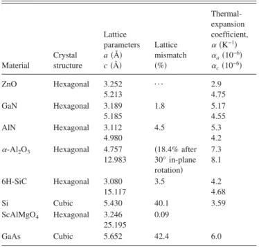
tions. Table II shows a comparison of measured and calcu-lated lattice parameters, c / a ratio, and u parameter reported by several groups for ZnO crystallized in wurtzite, zinc-blende, and rocksalt structures.
For the wurtzite ZnO, lattice constants at room tempera-ture determined by various experimental measurements and theoretical calculations are in good agreement. The lattice constants mostly range from 3.2475 to 3.2501 Å for the a parameter and from 5.2042 to 5.2075 Å for the c parameter. The data produced in earlier investigations reviewed by Reeber9are also consistent with the values given in Table II. The c / a ratio and u parameter vary in a slightly wider range, from 1.593 to 1.6035 and from 0.383 to 0.3856, respectively. The deviation from that of the ideal wurtzite crystal is prob-ably due to lattice stability and ionicity. It has been reported that free charge is the dominant factor responsible for ex-panding the lattice proportional to the deformation potential of the conduction-band minimum and inversely proportional to the carrier density and bulk modulus. The point defects such as zinc antisites, oxygen vacancies, and extended de-fects, such as threading dislocations, also increase the lattice constant, albeit to a lesser extent in the heteroepitaxial layers. For the zinc-blende polytype of ZnO, the calculated lat-tice constants based on a modern ab initio technique are predicted to be 4.60 and 4.619 Å. Ashrafi et al.72
character-ized the zinc-blende phase of ZnO films grown by plasma-assisted metal-organic molecular-beam epitaxy using reflec-tion high-energy electron-diffraction 共RHEED兲, x-ray-diffraction共XRD兲, transmission electron microscope 共TEM兲, and atomic-force microscope 共AFM兲 measurements. They have found that using a ZnS buffer layer led to the growth of the zinc-blende ZnO films. The lattice constants of the epil-ayer were estimated as 4.463, 4.37, and 4.47 Å by using the spacing of the RHEED pattern, albeit spotty, comparing the XRD peak position, and examining the TEM, respectively. These values are far from that of the wurtzite phase, indicat-ing the formation of zinc-blende ZnO. The lattice constant measured with the RHEED technique is in very good agree-ment with the theoretical prediction.
A high-pressure phase transition from the wurtzite to the rocksalt structure decreases the lattice constant down to the range of 4.271– 4.294 Å. The experimental values obtained by x-ray diffraction are in close agreement. The predicted lattice parameter of 4.058– 4.316 Å using various calculation techniques, such as the HF-PI, GGA, and HF, are about 5% smaller or larger than the experimental values. The discrep-ancy in the calculated values is larger than the measured ones.
Desgreniers64 has investigated whether the u parameter and the ideal correlation between u and c / a are affected by the compression of the ZnO wurtzite lattice. The change in c / a axial ratio was measured up to⬃10 GPa, and a pressure coefficient of d共c/a兲/dP=−0.0005±0.0001 GPa−1 was ob-tained from a linear fit 共giving c/a=1.6021 at atmospheric pressure兲 to the experimental data. Even though the variation with pressure seems within the experimental error, this pres-sure coefficient is in agreement with previously published experimental 关−0.0007 GPa−1 共Ref. 65兲兴 and predicted 关−0.0005 GPa−1 共Ref. 56兲兴 values. The effect of pressure-induced change of the axial ratio on the u parameter versus a possible breakdown of the ideal relationship between the axial ratio and u was isolated by recording the pressure-dependence variation of x-ray-diffraction intensity. It has been concluded that the ideal relationship between the c / a axial ratio and the u oxygen positional parameter is pre-served as the wurtzite lattice becomes denser while ap-proaching the structural transition pressure.
C. Electronic band structure
The band structure of a given semiconductor is pivotal in determining its potential utility. Consequently, an accurate knowledge of the band structure is critical if the semiconduc-tor in question is to be incorporated in the family of materials considered for device applications. Several theoretical ap-proaches of varying degrees of complexity have been em-ployed to calculate the band structure of ZnO for its wurzite, zinc-blende, and rocksalt polytypes. Besides, a number of experimental data have been published regarding the band structure of the electronic states of wurtzite ZnO. X-ray- or UV reflection/absorption or emission techniques have con-ventionally been used to measure the electronic core levels in solids. These methods basically measure the energy differ-ence by inducing transitions between electronic levels 共for
TABLE II. Measured and calculated lattice constants and u parameter of ZnO. Wurtzite a共Å兲 c共Å兲 c / a u Ref. 3.2496 5.2042 1.6018 0.3819 65a 3.2501 5.2071 1.6021 0.3817 59b 3.286 5.241 1.595 0.383 660c 3.2498 5.2066 1.6021 64d 3.2475 5.2075 1.6035 61e 3.2497 5.206 1.602 9f 1.593 0.3856 56g 1.600 0.383 661h Zinc blende 4.619,c4.60,g4.463,i4.37,i4.47i Rocksalt 4.271,a4.283,d4.294,e4.30,g4.280,j4.275,k 4.058,k4.316,k4.207,k4.225l
aMeasured by using x-ray diffraction. bMeasured by using x-ray diffraction.
cCalculated by using ab initio periodic linear combination of atomic orbitals 共LCAO兲 methods, based mainly on the Hartree-Fock Hamiltonian, with an all-electron Gaussian-type basis set.
dMeasured by using EDXD. eMeasured by using x-ray diffraction. fMeasured by using x-ray powder diffraction.
gCalculated by using first-principles periodic Hartree-Fock共HF兲 linear com-bination of atomic orbitals共LCAO兲 program.
hCalculated by using ab initio quantum-mechanical level through the Berry-phase scheme applied to delocalized crystalline orbitals and through the definition of well-localized Wannier functions.
iMeasured by using RHEED, XRD, and TEM共Ref. 72兲. jMeasured by using x-ray diffraction共Ref. 60兲.
kMeasured by using EDXD, and calculated using Coulomb-Hartree-Fock pertubed ion, GGA, and LDA methods共Ref. 62兲.
lCalculated by using first-principles periodic Hartree-Fock共Ref. 67兲.
example, transitions from the upper valence-band states to the upper conduction-band states, and from the lower valence-band states兲 or by exciting collective modes 共for ex-ample, the upper core states to the lower edge of the conduc-tion band and to excitaconduc-tions of plasmons兲. Another important method for the investigation of the energy region is based on the photoelectric effect extended to the x-ray region, namely, photoelectron spectroscopy 共PES兲. The peaks in emission spectrum correspond to electron emission from a core level without inelastic scattering, which is usually accompanied by a far-less-intense tail region in the spectrum. More recently, angle-resolved photoelectron spectroscopy 共ARPES兲 tech-nique has started to be used. This techtech-nique together with synchrotron radiation excitation has been recognized as a powerful tool that enables experimental bulk and surface electronic band-structure determinations under the assump-tions of k conservation and single nearly-free-electron-like final band.75After the theoretical work on band-structure cal-culation of ZnO proposed by Rössler using Green’s function 关Korringa-Kohn-Rostoker 共KKR兲 method兴76
in 1969, there have been several experimental works77–80performed on the wurtzite ZnO which proved Rössler’s predicted bulk elec-tronic structure to be far from satisfactory. Langer and Vesely77 have reported experimental data related to the en-ergy levels of core electrons in ZnO using x-ray-induced photoemission spectroscopy. They have drawn two conclu-sions from their studies:共i兲 the location of the Zn 3d level in ZnO has been unambiguously determined and 共ii兲 the dis-crepancy between the measured values and the theoretically determined energy values was angular momentum depen-dent. Powell et al.78,79 have carried out UV photoemission measurements on hexagonal ZnO cleaved in vacuum. Those authors have placed the Zn 3d core level at about 7.5 eV below the valence-band maximum, which is 3 eV lower than the value predicted by Rössler’s band calculation. This as-signment also showed good agreement with x-ray photo-emission results reported by Vesely et al.81共8.5 eV兲 and Ley et al.80 共8.81 eV兲. In the following years, LDA and tight-binding methods were employed82–85by considering the Zn 3d states as core levels to ease calculations. Satisfactory agreement with qualitative valence-band dispersions was achieved with this assumption. However, quantitative dis-agreements remained and the location of the Zn 3d states could not be predicted. Most recently, with the advent of computer capabilities, theoretical works have taken to in-clude the effect of the Zn 3d level in the calculations and thus to consider them as valence-band states.86–89 These methods enable an estimation of the position of the Zn 3d states and also take into account their non-negligible influ-ence on the s- and p-derived valinflu-ence bands.
Recently, Girard et al.90 have studied the electronic structure of the ZnO 共0001兲 surface by angle-resolved pho-toelectron spectroscopy. They recorded both normal and off-normal-emission spectra, which give valuable information about bulk and surface states as well as the Zn 3d states. Figure 6 shows some of the normal-emission spectra re-corded at photon energies ranging from 20 to 50 eV and the information extracted from these data for bulk-band struc-ture. In these measurements, the binding energies were
re-ferred to the Fermi level and the intensities were normalized to the photon flux. Among all the spectra displayed, seven features were seen, labeled from A to G. The dispersions of the four valence bands observed in the共0001兲 direction were compared with theory based on LDA calculations, which consider the Zn 3d electrons as part of the valence band,86 and good agreement was realized. It should also be noted that the Zn 3d states were observed to separate into two groups of four and six bands, which show dispersion with k, which is in agreement with theoretical results, but the loca-tion of these states 共about 10.5 eV below Fermi level兲 were not accurately predicted.
FIG. 6. 共a兲 Normal-emission spectra for photon energies ranging from 20 to 50 eV. The spectra were normalized with respect to the photon flux. 共b兲 The bulk-band structure of ZnO, ⌫A corresponding to 0.6 Å−1. 关Re-printed from R. T. Girard, O. Tjernberg, G. Chiaia, S. Söderholm, U. O. Karlsson, C. Wigren, H. Nylèn, and I. Lindau, Surf. Sci. 373, 409共1997兲, Copyright 1997, with permission from Elsevier.兴 The dashed lines are the LDA calculation results reproduced from Schröer et al.共Ref. 86兲.
The polar共0001兲-Zn and 共0001¯兲-O surfaces and the non-polar共101¯0兲 surface 共m plane兲 have also been the object of experimental and theoretical investigations. Of these sur-faces, the nonpolar 共101¯0兲 surface is of particular interest from the viewpoint of surface chemistry, because the surface is terminated with the same number of O and Zn atoms. The low-energy electron-diffraction 共LEED兲 studies have re-vealed that the surface undergoes relaxation, which is char-acterized by downward shift 共spatially兲 of both surface Zn and O atoms, with a greater shift for the Zn atom than the O atom, resulting in the Zn–O bond rotation by 6.2°共Ref. 91兲 or 11.5° 共Ref. 92兲 with respect to the ideal surface plane. Such a surface relaxation should influence the energetic po-sition as well as the dispersion width of the surface dangling-bond bands of the occupied O 2p and unoccupied Zn 4s states. Besides, several theoretical studies have indicated that, upon relaxation, the O 2p dangling-bond state is stabi-lized while the Zn 4s dangling-bond state shifts up in energy.84,88,93The theoretically determined position of these dangling-bond bands, especially the occupied O 2p dangling-bond band, relative to the bulk bands projected onto the共101¯0兲 surface varies depending on the method em-ployed in the calculations.
A detailed experimental study applied to both polar and nonpolar surfaces of ZnO has been carried out by Göpel et al.94using ARPES. They have identified two surface-induced features at the ⌫, M, and X points of the surface Brillouin zone共BZ兲 and have assigned these states to the O 2p-derived dangling-bond state and the Zn–O back-bond state. Zwicker and Jacobi95 have also performed the ARPES study on the ZnO 共101¯0兲 surface and have revealed the valence-band structure along the ⌫M axis of the bulk BZ. In this experi-ment, however, a surface-related state was not identified and all the observed peaks were attributed to the bulk-band tran-sitions. Recently, the off-normal ARPES spectra in the ⌫¯M¯ , ⌫¯K¯, and K¯M¯ directions were recorded for 20, 34, and 44 eV photon energies at emission angles ranging between 0° and 30° by Girard et al.90From these measurements, two surface states were observed on the 共0001兲 surface. One state, at 7.5 eV binding energy, which was also predicted by theory, was interpreted as arising from the “backbonding” of the Zn 4s-O 2p mixed bulk states. The other one, at 4.5 eV below Fermi level, which was not predicted by theoretical calculations, was related to Zn 4p-O 2p derived states.
More recently, detailed ARPES studies were performed to investigate the two-dimensional band structure of the O 2p dangling-bond state on the ZnO 共101¯0兲 surface along the selected high-symmetry axes of the surface BZ, i.e., the⌫¯X¯ and ⌫¯X¯
⬘
axes.96 The energetic position relative to the pro-jected bulk bands and the dispersion width of the dangling-bond band were determined and compared with the calcu-lated band structures by Wang and Duke93and by Schröer et al.88 Figure 7 shows off-normal-emission spectra taken at various detection angles along the 关12¯10兴 共⌫¯X¯兲 and 关0001兴 共⌫¯X¯⬘
兲 azimuths and measured dispersion of the O 2pFIG. 7. 共a兲 Off-normal-emission spectra of the clean surface recorded at h= 22.5 eV and i= 55° along the 关12¯10兴 共⌫¯X¯兲 direction and at h
= 27 eV andi= 55° along the关0001兴 共⌫¯X¯⬘兲 direction. The incidence plane
of the light was parallel to the关12¯10兴 direction for both detection directions. The spectra are shown with 2° interval. The peak positions, indicated by the vertical bars, were determined from the second derivative of the spectra. The position of the valence-band maximum was determined from the normal-emission spectrum taken at h= 17 eV by extrapolating the onset of the valence-band emission as shown in the inset of the right panel. 共b兲 The measured dispersion of the O 2p dangling-bond state共open circles兲 and the bulk-band-related states 共filled circles兲 along the ⌫¯X¯ and ⌫¯X¯⬘ axes. The hatched area corresponds to the projected bulk-band region and the bold dashed line indicates the O 2p dangling-bond bands, both of which have been calculated using the sp3model by Wang and Duke共Ref. 93兲. The thin dashed lines which are located above the projected bulk bands are the dangling-bond bands obtained from the LDA calculations.关Reprinted with permission from K. Ozawa, K. Sawada, Y. Shirotori, K. Edamoto, and M. Nakatake, Phys. Rev. B 68, 125417共2003兲. Copyright 2003 by the Ameri-can Physical Society.兴
dangling-bond state and the bulk-band-related states along the⌫¯X¯ and ⌫¯X¯
⬘
axes together with theoretical calculation for comparison.From photon-energy-dependent measurements and K and O2adsorption studies it has been found that the surface-localized O 2p dangling-bond state exists at 3.7 eV below the Fermi level at the ⌫¯ point in the surface Brillouin zone and shifts to the higher-binding-energy side by 0.8 and 0.5 eV along the ⌫¯X¯ and ⌫¯X¯
⬘
axes, respectively. Measure-ments on K- and O2-exposed ZnO共101¯0兲 surfaces helped to identify which peaks in the angle-resolved photoelectron spectra were associated with the states localized at the sur-face. The O 2p dangling-bond band was found to be located below the upper edge of the projected bulk bands along these two high-symmetry axes. The empirical tight-binding calcu-lations performed by Ivanov and Pollmann84 and by Wang and Duke,93which emphasize the ionic and covalent charac-ters of the Zn–O bonds, respectively, predict that the gap state by the O 2p dangling bond is not formed at least along the⌫¯X¯ and ⌫¯X¯⬘
axes. On the other hand, Schröer et al. have found in their LDA study that the dangling-bond band is formed within the gap above the upper edge of the projected bulk bands along the major high-symmetry axes of the sur-face BZ. Therefore, it has been concluded that the experi-mental study is consistent qualitatively with the band struc-ture given by the two empirical tight-binding approaches.The theoretical calculation of the band structure of ZnO mostly involve the LDA,86,97–99 which is very demanding because of the cationic d electrons. If the d electrons are treated as core electrons, the calculated lattice constant un-derestimates the experimental values by as much as 18% for wurtzite ZnO, while inclusion of the d electrons in the va-lence band yields very accurate lattice constants. However, even if the d electrons are properly taken into account, the results of standard LDA calculations show distinct shortcom-ings, such as strongly underestimated band gap and overes-timated occupied cationic d bands, which roughly reside 3 eV high in energy as compared to experiment. In addition, their interactions with the anion p valence bands are artifi-cially enlarged, resulting in overestimated dispersion and bandwidth of the latter and shifting them unphysically close to the conduction bands. For example, the LDA underesti-mates the ZnO band gap to be as low as EgLDA= 0.23 eV, as
opposed to Egexp= 3.37 eV. Zakharov et al.
100
have recently reported plane-wave GW method for a number of II-VI com-pounds. They simply treated the d electrons as core electrons and deliberately carried out their GW calculation at the ex-perimental lattice constants. They obtained very good results for the anion p valence bands and for the band-gap energies but no assertion concerning the d-band positions could be made. Recently, Vogel et al.89 suggested an alternative ap-proach to treat the II-VI semiconductor compounds, which approximately incorporates dominant self-interaction correc-tions. It has been shown that self-interaction corrections to LDA can be very important for a quantitative description of a system with strongly localized states such as 3d electrons. Their results along with the previous LDA calculations and the O 2p valence bands are shown in Fig. 8 in more detail
with the ARPES data for comparison. The left panel in 共a兲 shows the standard LDA result, which reveals the above-mentioned shortcomings. The right panel shows the band structure as calculated with the self—interaction corrected pseudopotential 共SIC-PP兲 approach included in the LDA. It has been observed that the d bands are shifted down in en-ergy considerably and concomitantly the band gap is opened drastically. The dispersion and bandwidth of the O 2p are also changed. As compared to experimental data, the stan-dard LDA result is obscured by the artificially high-lying bands leading to strong p-d interactions with the O 2p bands. The SIC-PP results are in better agreement with experiments. The calculated and measured energy gaps, the position of the cation d band, and anion valence bandwidths of ZnO are given in Table III. Based on this table, the LDA-SIC-PP approximation gives close agreement with the experimental results for band gap and bandwidth compared to the standard LDA method. However, the d bands result in energy roughly 1 eV too low as compared to the experimental value. This
FIG. 8. 共a兲 LDA bulk-band structure of ZnO as calculated using a standard pseudopotential共PP兲 共left panel兲 and using SIC-PP 共right panel兲. The hori-zontal dashed lines indicate the measured gap energy and d-band width.共b兲 Comparison of the calculated and measured valence bands of ZnO. The left panel shows the standard LDA, while the right panel shows the SIC-PP results.关Reprinted with permission from D. Vogel, P. Krüger, and J. Poll-mann, Phys. Rev. B 52, R14316共1995兲. Copyright 1995 by the American Physical Society.兴
deviation was attributed to the measured exciton energies influenced by electronic relaxations, which is expected to be mostly pronounced for the highly localized cationic semicore d states.
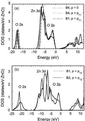
The electronic band structure of the other phases of ZnO has also been studied by a number of researchers.56,57,101,102 For example, recently, Jaffe et al.57 utilized both the LDA and the PBE96 form of the GGA together with optimized Gaussian basis sets to expand the crystal orbitals and peri-odic electron density in order to calculate the electronic structure for ZnO in the B4共wurtzite兲, B3 共zinc blende兲, B1 共rocksalt兲, and B2 共CsCl兲 crystal structures over a range of unit-cell volumes. Figures 9 and 10 show the calculated band structure and the total density of states 共DOS兲 of ZnO for different phases. When wurtzite ZnO is compressed, it has been observed that the peak at the top of the upper valence band is slightly reduced in height and shifted down in en-ergy, the O 2s- and Zn 3d-derived peaks are slightly broad-ened and shifted up in energy, and a splitting appears in the Zn 3d states. While transforming to the B1 structure at the transition pressure pT1, significant changes have been ob-served, in particular, the peak near the valence-band maxi-mum is greatly reduced in height. The Zn 3d peak also be-comes narrower, and the O 2s-derived states drop slightly in energy. Upon compression of the B1-phase ZnO through the wide pressure range from pT1 to pT2, it has been observed that the upper valence band broadens greatly, the splitting of the Zn 3d peak in the DOS shows a large increase, and the O 2s-derived band moves down in energy and broadens. The fundamental band gap also increases with increasing pres-sure in this range. With the B1→B2 transition, the upper valence bandwidth remains almost unchanged but the peak near the valence-band maximum reappears. The structure of
the Zn 3d states changes radically with the O 2p-derived states because of heavy hybridization, and the O 2s-derived states broaden further and shift up in energy. From these observations of ZnO band structure with compression and changed atomic coordination it has been argued that the key features are共a兲 changes in nearest-neighbor bond lengths as they affect overlaps and bandwidths and共b兲 changes in sym-metry as they affect p-d hybridization and band repulsion. As the neighboring atoms approach each other with compression of the solid, basis functions 共and orbitals in a Hückel-like picture103兲 overlap more strongly, producing increased dis-persion of the electron bands in k space and consequently increased bandwidths along the energy axis. However, it has also been considered that when there is a phase transition to a structure of increased coordination, the nearest-neighbor bonds lengthen even though the density is increased. The behavior of the bandwidths up to pT2reflects these consider-ations. The band structures reveal further qualitative changes that occur with the change of symmetry at the structural tran-sitions. Where the symmetry permits hybridization of O 2p-and Zn 3d-derived b2p-ands, there is an effective repulsion be-tween them, which pushes the anion 2p states upwards. In the tetrahedrally coordinated B4 phase this repulsion is present throughout the Brillouin zone, but in the cubic B1 and B2 structures it is suppressed near the⌫ point as a result of the inversion symmetry through the atomic center. Conse-quently, the highest valence bands are repelled upwards near the zone boundaries but not at the zone center, so that the valence-band maximum now occurs at the zone boundary. This accounts for the change in shape of the band edge seen in the total DOS plots. There is also a change in the form of
TABLE III. Calculated and measured energy gaps Eg, cation d-band
posi-tions Ed, and anion p valence bandwidths Wp共in eV兲 of ZnO 关Vogel et al.
共Ref. 89兲兴. PP, local-density approximation pseudopotential; LDA-SIC-PP, local-density approximation self-interaction-corrected pseudopoten-tial.
LDA-PP LDA-SIC-PP Expt.
Eg 0.23 3.77 3.4
Ed −5.1 −8.9 −7.8
Wp −3.99 −5.2 −5.3
FIG. 9. Band structures for ZnO:共a兲 B4 structure at p=0, 共b兲 B1 structure at p = pT1, and共c兲 B2 structure at p=pT2.关Reprinted with permission from J. E. Jaffe, J. A. Snyder, Z. Lin, and A. C. Hess, Phys. Rev. B 62, 1660共2000兲. Copyright 2000 by the American Physical Society.兴
FIG. 10. Total density of states共DOS兲 for ZnO in the 共a兲 B4 structure at p = 0 and p = pT1, B1 structure at p = pT1, and共b兲 B1 and B2 structures at p = pT2.关Reprinted with permission from J. E. Jaffe, J. A. Snyder, Z. Lin, and
A. C. Hess, Phys. Rev. B 62, 1660共2000兲. Copyright 2000 by the American Physical Society兴.
the Zn 3d-derived bands, which are now narrowest near the ⌫ point as a result of the suppressed hybridization there. In the B2 structure the Zn 3d and O 2p states are completely hybridized and cannot be disentangled.
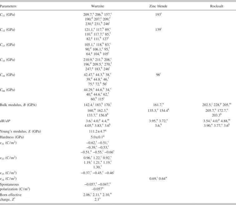
D. Mechanical properties
The mechanical properties of materials involve various concepts such as hardness, stiffness, and piezoelectric con-stants, Young’s and bulk moduli, and yield strength. In hex-agonal crystals, there exist five independent elastic constants: C11, C33, C12, C13, and C44. Elastic constants C11 and C33 correspond to longitudinal modes along the 关1000兴 and 关0001兴 directions, respectively. Elastic constants C44 and
C66=共C11− C12兲/2 共owing to symmetry兲 can be determined from the sound velocity of transverse modes propagating along the关0001兴 and 关1000兴 directions, respectively. The re-maining constant C13 is present in combination with four other moduli in the velocity of modes propagating in less-symmetrical directions, such as关0011兴. The bulk modulus is related to the elastic constants by104
B = 共C11+ C12兲C33− 2C13
2
C11+ C12+ 2C33− 4C13. 共3兲
Although the wurtzite ZnO crystal is acoustically aniso-tropic, there is only a very small difference between the shear sound velocitiesTA1 andTA2 propagating along the 关001兴 and 关100兴 directions, respectively 共TA2/TA1⬵0.98兲. In the isotropic approximation, the Young modulus E and shear modulus G can also be evaluated using the relations E = 3B共1−2兲 and G=E/2共1+兲, respectively. The termis the Poisson ratio and is given by= C13/共C11+ C12兲.
It has been argued that the most precise technique used to determine the elastic moduli of compound materials is ultrasonic measurement, which requires thick single-crystalline samples, about 1 cm thick, to enable precise mea-surement of the time required for the plane-wave acoustic pulses to propagate through the crystal.105The quasilongitu-dinal and quasishear wave velocities can be used in the fol-lowing equation to calculate C13:105
C13= 1
cos␣sin␣关共22−V兲共33−V
2兲兴1/2− C
44, 共4兲 where, for hexagonal symmetry,
22= C11cos2␣+ C44sin2␣,
共5兲 33= C44cos2␣+ C33sin2␣.
Here ␣ is the angle between the propagation direction and the c axis,is the mass per unit volume, and V is either the quasilongitudinal or the quasishear velocity.
As an optical technique, Brillouin scattering allows the determination of the elastic constants and hence of the bulk moduli through the interaction of light with thermal excita-tion in a material, in particular, acoustic phonons in a crystal. In this technique, the elastic constants C11 and C66 can be directly obtained from measurement of the phase velocity of the longitudinal mode and of the shear horizontal mode trav-eling parallel to the crystal surface. The remaining constants,
C13, C33, and C44, can be evaluated from measurement of the phase velocity of the Rayleigh surface wave and of the lon-gitudinal bulk acoustic wave propagating at different angles from the surface normal. Various forms of x-ray diffraction, such as energy-dispersive x-ray diffraction 共EDX兲 , angular dispersive x-ray diffraction 共ADX兲 , and x-ray-absorption spectroscopy共XAS兲, can also be employed to determine the pressure dependence of the lattice parameters. From that, ex-perimental equation of state共EOS兲, a widely used approach being the Murnaghan equation of state and hence directly the bulk modulus, which is based on the assumption that the bulk modulus has a linear dependence on pressure P, can be deduced as106 V = V0
冉
1 + B⬘
P B冊
1/B⬘ , 共6兲where B and V0represent the bulk modulus and unit volume at ambient pressure, respectively, and B
⬘
is the derivative of B with respect to pressure. X-ray diffraction leads to the determination of the isothermal bulk modulus, whereas Bril-louin scattering leads to the adiabatic one. Nevertheless in solids other than molecular solids there is no measurable difference between the two thermodynamic quantities. Be-sides the experimental investigations, many theoretical cal-culations have also been employed to determine the struc-tural and mechanical properties of ZnO. Most of the calculations are based on density-functional theory within the LDA using various types of exchange-correlation func-tionals, and either plane-wave expansion for the pseudopo-tentials or the LMTO method.Among the tetrahedrally bonded semiconductors, it has been stated that ZnO has the highest piezoelectric tensor or at least one comparable to that of GaN and AlN.107This prop-erty makes it a technologically important material for many applications, which require a large electromechanical cou-pling. The piezoelectric tensor has three independent compo-nents in hexagonal wurtzite phase and one共e14兲 in the cubic zinc-blende phase, which characterize the full piezoelectric tensors of such crystals.108 Two of these components in wurtzite phase measure the polarization induced along the c axis, at zero electric field, by a uniform strain either along the c axis or in the basal plane. The relevant relationship is109
Pz
piezo
= e33z+ e31⬜, 共7兲
where z and⬜ are the strain along the c axis and in the
basal plane, respectively. e33 and e31 are the piezoelectric coefficients. The third independent component of the piezo-electric tensor, e15, describes the polarization induced by a shear strain which is usually neglected for simplicity. The sign of the piezoelectric tensor is generally fixed assuming that the positive direction along the c axis goes from the cation to the anion.
The natural structure of ZnO is wurtzite, which has a low symmetry, resulting in the existence of spontaneous po-larization along the c direction. However, the absolute value of the spontaneous polarization in a nonferroelectric material has never been directly measured, while one invariably mea-sures the polarization derivatives. In semiconductors, the
spontaneous polarization may be deduced by investigating the two-dimensional electron gas and the redshift of the tran-sitions in quantum wells albeit indirectly. From the theoreti-cal point of view, there have been some efforts in determin-ing the value of the spontaneous polarization in ZnO. One conventional approach is to define the spontaneous polariza-tion of a low-symmetry crystal共wurtzite兲 as the polarization difference with respect to a high-symmetry structure 共zinc blende兲 of the same material.
The micro- and nanoindentation methods are widely used in the determination of hardness of ZnO over a wide range of size scales and temperatures. Hardness measure-ments are usually carried out on the 共0001兲 surface of the crystal using the conventional pyramidal or spherical dia-mond tip, or alternatively, with a sharp triangular indenter. The depth-sensing indentation measurements provide the complete information on the hardness and pressure-induced phase transformation of semiconductor materials. Table IV shows the measured and calculated mechanical parameters reported by several groups for ZnO crystallized in the form of wurtzite, zinc-blende, and rocksalt.
For ZnO, it seems that theoretical predictions are in good agreement with experimental findings for certain bulk mate-rial properties. The quality of the crystals and theoretical approximations are of primary importance for the precise determination of the physical properties. In regard to the elastic constants, theory and experiments seem capable of producing data which are quite consistent for wurtzite-phase ZnO. Bulk modulus and its rate of change with pressure for all phases are in good agreement within the various experi-mental findings as well as the theoretical predictions with a few exceptions. Any dispersion might be due to the sample quality, the accuracy of each experimental method, and pho-non dispersion. Each calculation method also has its own limitations related to the basic material parameters, basis sets, and the precisions used in addition to the approxima-tions of the method itself, leading to variaapproxima-tions in the calcu-lated parameters. As compared to group-III-nitrides共e.g., for GaN, C11= 296 GPa, C12= 130 GPa, C13= 120 GPa, C33 = 395 GPa, C44= 241 GPa, and B = 190– 245 GPa兲,110 the elastic and bulk moduli of ZnO are small. Recent ultrasonic experiments on single-crystal specimens of the wurtzite共B4兲 phase of ZnO have shown that, under pressure, this material becomes softer against shear-type acoustic distortions.
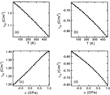
Decremps et al.111have studied the pressure behavior of both longitudinal共C11and C33兲 and transverse 共C44and C66兲 elastic moduli for the wurtzite phase of single-crystal ZnO using ultrasonic wave velocity measurements up to 10 GPa at three different temperatures. As shown in Fig. 11, it has been observed that all the moduli exhibit a linear dependence on pressure up to the phase-transition pressures, with posi-tive values for the room-temperature longitudinal moduli 共dC11/ dP = 5.32 and dC33/ dP = 3.78兲 but negative values for the shear moduli共dC44/ dP = −0.35 and dC66/ dP = −0.30兲. At high temperatures, the pressure derivatives of the elastic shear modes become more negative. Thus, the elastic shear softening observed at room temperature is enhanced at el-evated temperatures. The effect of phonons and the role of bond-bending forces as a function of pressure in causing the
elastic softening were investigated. It has been observed that the pressure at which the phase transition 共B4–B1兲 com-mences decreases to about 6 GPa at 600 ° C as compared to 7.5 GPa at room temperature.
In an earlier study, similar pressure dependence was also reported by Soga and Anderson112 who measured the pres-sure derivatives of the room-temperature longitudinal 共L兲 and transverse 共T兲 sound velocities of polycrystalline ZnO. They obtained 共L/P兲T= 3.643 310 23 km/ s kbar and
共T/P兲T= 23.193 310 23 km/ s kbar, corresponding to
共B /P兲T= 4.8 and共G /P兲T=−0.71 共B is the bulk modulus
and G is the shear modulus兲. On the theoretical side, a linear evolution under pressure was calculated for the two longitu-dinal modes, C11 and C33, with pressure derivatives of 3.18 and 1.72, respectively, using atomistic calculations based on an interatomic pair potential within the shell-model approach.70The shear moduli C44and C66exhibited negative pressure dependence with pressure derivatives of −0.30 and −0.84, respectively. The experimental and calculated values slightly disagreed. The unusual negative values for both shear modes were attributed to two simultaneous effects:111 共i兲 a major contribution of the second-nearest-neighbor inter-actions to the transverse-acoustic-phonon modes and 共ii兲 an enhancement of the Coulomb forces screening between an atom and its second-nearest neighbor. Another explanation for the observed shear softening of ZnO was related to the decrease of bond-bending forces.
The deformation behavior of bulk ZnO single crystals was studied by a combination of spherical nanoindentation and atomic-force microscopy.113ZnO exhibited plastic defor-mation for relatively low loads 共⬎4–13 mN with an ⬃4.2-mm radius spherical indenter兲. The average contact pressure hardness H and Young’s modulus E as a function of indenter penetration were determined by analysis of partial load-unload data. The hardness value of ZnO is measured as 5.0± 0.1 GPa at a plastic penetration depth of 300 nm. The Young modulus remains essentially constant over the in-denter penetration depth, with E = 111.2± 4.7 GPa. Previous indentation studies performed mostly on polycrystalline ZnO have reported a wide range of H 共⬃1.5–12 GPa兲 and E 共⬃40–120 GPa兲 values. However, it should be noted from these results that ZnO is significantly softer than GaN, where H 共GaN兲=15.5±0.9 GPa and E 共GaN兲=210±23 GPa.113 The lower value of H for ZnO is, in fact, expected due to a lower melting point共1975 °C兲 and larger ionicity 共0.616兲 as compared to that of GaN共2500 °C and 0.500兲.114
The spontaneous and piezoelectric polarization in ZnO have been studied theoretically by a number of groups and compared with a few available indirect experimental results. Dal Corso et al.107demonstrated the feasibility of ab initio studies of piezoelectricity within an all-electron scheme. A comparative analysis was performed in order to understand the microscopic origin of the peculiar behavior of ZnO. They have concluded that the piezoelectric effect results from two different contributions of opposite signs, which were referred to as the “clamped ion” and “internal strain.” It has been shown that the large piezoelectric tensor of ZnO is due to the low value of its clamped-ion contribution共reducing the can-celation effect兲; besides, the piezoelectric tensor is