Interaction of Adatoms and Molecules with Single-Layer Arsenene
Phases
Fatih Ersan,
†Ethem Aktürk,
*
,†,‡,§and Salim Ciraci
*
,§†Department of Physics and‡Nanotechnology Application and Research Center, Adnan Menderes University, Aydın 09010, Turkey §Department of Physics, Bilkent University, Ankara 06800, Turkey
ABSTRACT: Recent studies have shown that arsenic can form single-layer phases in buckled honeycomb as well as symmetric washboard structures, named as arsenene. These structures are stable even in freestanding form and are nonmagnetic semiconductors in the energy range which is suitable for various electronic applications. In this study we investigated the adsorption of selected adatoms (H, Li, B, C, N, O, Al, Si, P, Cl, Ti, Ga, Ge, As, Se, and Sb) and physisorption of molecules (H2, O2, and H2O) to these two arsene phases. Since the interaction of these adspecies with arsenene are studied using large supercells, the coupling between adspecies is minimized, and hence our results can be interpreted to mimic the effects of isolated adatom or physisorbed molecule. It is found that the adatoms form strong chemisorption bonds and hence modify the atomic structure and physical properties locally. Some of the adatoms give rise to significant local reconstruction of the atomic structure. Electronic states of some adatoms become spin polarized and attain net magnetic moments; they may even
display half-metallic character at high coverage. A majority of adsorbed atoms give rise to localized states in the fundamental band gap. We showed that the interactions between H2, O2, and H2O molecules and single-layer arsenene are rather weak and do not
cause any significant changes in the physical properties of these molecules, as well as those of arsenene phases. However, some of these molecules can be dissociated at the edges of theflakes of arsenene structures; their constituents are adsorbed to the edge atoms and cause local reconstructions.
■
INTRODUCTIONRecently, single-layer (SL) structures of group V elements or pnictogens (N, P, As, Sb, Bi) have been the subject of active theoretical and experimental research.1−6On the basis of first-principles density functional theory7(DFT) calculations it has been shown that arsenic can form SL two-dimensional (2D) structures, named as arsenene.4 These are a buckled honey-comb structure (b-arsenene or b-As), where As atoms at the corners of the hexagon rise and lower alternatingly to make two As atomic planes like SL silicene,8,9and a symmetric washboard structure (w-arsenene or w-As) as shown inFigure 1a and1b. These new SL structures of arsenic with semiconducting properties have attracted considerable interest in flexible 2D electronics, photocatalytic applications, and nanomaterial fabrication. Now efforts have focused to synthesize these phases.10
Earlier, it has been shown experimentally and theoretically that bare SL structures can be functionalized through adsorption of adatoms to attain crucial physical and chemical properties for diverse applications.11−18 For example, while graphene is inert to H2 molecule, each Ti, Li, or Ca adatom adsorbed to graphene can hold 4−5 H2molecules, providing an excellent high-capacity medium of hydrogen storage.12,14Those properties have been shown to be strongly dependent on the coverage of adatoms to lead to tunable electronic properties. Accordingly, these unusual electronic, magnetic, and chemical
properties achieved through the adsorption of foreign atoms to SL honeycomb structures have provided important applications and hence have augmented the interest in bare structures. In this respect, while bare arsenene phases are predicted to be semiconducting nanostructures, their physical properties are expected to be modified to a large extent by the adsorption of adatoms. Similarly, physisorption of molecules followed by their dissociation at the edges or defect sites have resulted in interesting hydrogen evolution reactions19,20 and reversible oxidation−deoxidation reactions.21 Interplay between applied electric field and desorption has been another interesting feature revealed in the study of the interaction between SL structures and adatoms.21,22More recently, functionalization or doping of one of two arsenene structures, namely, only b-As or w-As, by adsorption23or substitution24−26of a relatively smaller number of selected atoms has been investigated.
This paper presents an extensive analysis of the effects of chemisorbed adatoms (H, Li, B, C, N, O, Al, Si, P, Cl, Ti, Ga, Ge, As, Se, and Sb) and physisorbed molecules (H2, O2, and
H2O) on the physical properties of two SL arsenene phases. In
earlier studies, these adatoms have been shown to engage in chemical interactions with various SL structures, like graphene,
Received: March 8, 2016
Revised: June 15, 2016
Published: June 15, 2016
Article pubs.acs.org/JPCC
Downloaded via BILKENT UNIV on December 23, 2018 at 08:04:30 (UTC).
silicene, BN, MoS2, etc., and give rise to novel chemical and physical functional properties. Additionally, one-half of these adatoms by themselves form SL honeycomb structures. Also, most of these elements are constituents of a 3D crystal in diamond and zincblende structure showing well-known electronic and optical properties. Titanium can be an important element in high-capacity H2 storage when adsorbed on SL
structures. Owing to a large number of atoms and molecules included in our analysis, we treated only the effects of adsorption of single (isolated) adatoms and physisorbed single molecules on the atomic structure and electronic properties of arsenene. Coverage-dependent properties with different cover-age and induced overlayer structure are beyond the scope of the present paper.
We found that (i) H2, O2, and H2O molecules neither form strong chemical bonds with SL arsenene nor dissociate; they are physisorbed with a weak binding energy without affecting the properties of arsenene significantly. However, H2and O2
molecules strongly interact with 2-fold-coordinated active sites at the edges of arseneneflakes and subsequently are dissociated into constituent atoms. (ii) On the other hand, single adatoms, H, Li, B, C, N, O, Al, Si, P, Cl, Ti, Ga, Ge, As, Se, and Sb, are adsorbed with significant binding energy ranging from 1.03 to 4.58 eV. While some of these adatoms, namely, C and B, substitute a host As atom of arsenene by pushing it downward, some of them, namely, Si, P, Ti, and As, create massive local reconstruction in 2D SL arsenene. Some adatoms attain significant magnetic moments, while a majority of them exchange a significant amount of charge with arsenene. (iii) Most of the adatoms treated here have localized states near the band edges and attribute crucial electronic properties to arsenene.
■
COMPUTATIONAL DETAILSWe carried out calculations within supercell geometry using periodic boundary condition. Each supercell is constructed from (n× n) primitive cells of b-As and w-As. One adatom is placed at the same position of each supercell, so that adsorbed adatoms formed a regular array. The coupling between adjacent adatoms decreases with increasing n. The size of the supercell, namely, n, is determined by calculating the binding energy of selected adatoms, C, P, and Al, adsorbed on n = 3, 4, and 5 supercells. The average difference between the binding energies for n = 4 and 5 was smaller than 17 meV. In view of this analysis, we performed all calculations using (4× 4) supercell for b-As and (3× 4) supercell for w-As. Physisorbed molecules also are treated using similar supercells. In these supercells smallest separations between adatoms or physisorbed mole-cules on the b-As and w-As phases attained distances of lb = 14.39 Å and lw = 14.16 Å, respectively. The vacuum spacing
between SL structures, i.e., the lattice constant of the supercell perpendicular to b-As as well as w-As, is taken as 20 Å. Supercell geometry is also used in the calculations using small flakes of arsenene, where a vacuum spacing of 20 Å is taken between adjacentflakes.
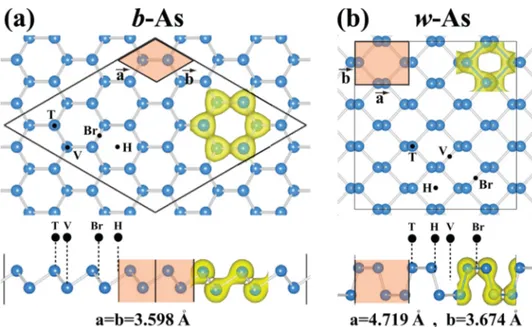
Figure 1describes our models of supercells for b-As and w-As phases and possible adsorption sites. For b-As, the adatom on top of the host As atoms is specified as the top (T) site. The bridge (Br) site is above the center of the As−As bond. The hollow (H) site is located above the center of hexagons of the host As atoms. At the valley (V) site, the adatom is placed on top the low-buckled host As atoms. For the w-site, similar sites are also indicated inFigure 1. The equilibrium structure of each adspecies and the corresponding atomic configuration including the substrate are determined following a comprehensive optimization process. First, each adatom or molecule is placed to all possible sites described in Figure 1 at a distant height from the SL substrate. Subsequently, all atomic positions Figure 1.(a) Top and side views of the optimized atomic configuration of the (4 × 4) supercell of b-As phase used to treat the adsorbed single adatom. Two-dimensional hexagonal primitive unit cell with lattice constants a = b is shaded and delineated by thick lines. Possible adsorption sites are the top site (T), where the adatom is on top of the host As atoms, the bridge site (Br), where the adatom is above the center of the As−As bond, the hollow site (H), where the adatom is located above the center of hexagons of the host As atoms, and the valley site (V), where the adatom is placed on top the low-buckled host As atoms. Total charge density isosurfaces show bonds between nearest As atoms. (b) Top and side views of the atomic configuration of the (3 × 4) supercell of w-As used to treat the adsorbed single adatom. Two-dimensional rectangular primitive unit cell, lattice constants and isosurfaces of the total charge density are also shown.
including the height of the adatom or molecule and atomic positions of substrate atoms are relaxed to attain the minimum total energy, ET[substrate + A(M)]. Here A(M) denotes
adatom (molecule). Then the binding energy Eb (or
physisorption energy, Ea) is obtained from the expression
Eb(Ea) = ET[subs] + ET[A(M)]− ET[subs + A(M)] in terms of the total spin-polarized energies of the free adatom (molecule) of bare substrate and of the system of adatom adsorbed (molecule physisorbed) to the substrate. The positive value of Eb(Ea) indicates that the binding of adatom (physisorption of
molecule) to arsenene is favorable for a given geometry. Since the initial configuration relative to the substrate is crucial for physisorbed molecules, various orientations have been also tested to achieve the highest physisorption energy. It should be noted that adatoms which have minute couplings with nearest adatoms in adjacent supercells for large n can mimic the chemisorption of a single atom on a large arsenene substrate (or dilute coverage Θ ≪ 1). On the other hand, adatoms treated using small n lead to high coverage,Θ ≈ 1, resulting in a specific decoration, whereby the interaction between single adatom and substrate and hence the physical properties thereof are modified significantly depending on the coverage Θ. For example, at high coverage the localized electronic states originated from adatoms can form energy bands. In the present case, small adatom−adatom coupling lets us interpret our results as if a single, isolated impurity (or dilute doping).
We performed first-principles, pseudopotential plane wave calculations based on the spin-polarized DFT7 within the generalized gradient approximation including van der Waals (vdW) corrections.27Here we used projector-augmented wave (PAW) potential,s28and the exchange-correlation potential is
approximated with the Perdew−Burke−Ernzerhof (PBE)
functional.29 Numerical calculations were carried out using the VASP software.30On the basis of the convergence analysis on kinetic energy cutoff and k-point sampling, a plane-wave basis set with kinetic energy cutoff is taken to be ℏ2|k + G|2/2m
= 500 eV and the Brillouin zone (BZ) was sampled in the
k-space within the Monkhorst−Pack scheme31by (7 × 7 × 1) mesh. Atomic positions were optimized using the conjugate gradient method, where the total energy and atomic forces were minimized. The energy convergence value between two consecutive steps was chosen as 10−5 eV, and a maximum force of 0.002 eV/Å was allowed on each atom. A Gaussian-type Fermi-level smearing method is used with a smearing width of 0.01 eV. The total energies and energy bands of bare and adatom adsorbed (molecule physisorbed) SL, b-As, and w-As structures are calculated by using PBE. In view of the fact that energy band gaps are underestimated by DFT, we corrected band energies using the HSE06 (HSE) method32−34 The magnetic ground states of adatom + substrate systems revealed by the optimization based on spin-polarized DFT are further elaborated. To this end, calculations are performed by optimizing the total energy for preset magnetic moments to prevent the system from pinning erroneously at a magnetic moment. Then the magnetic moment of the system corresponding to the minimum total energy has been taken as the magnetic moment of the system. This is the well-known and most rigorous method used in the calculation of magnetic states. To prevent the system from pinning erroneously at a magnetic moment, charge transfer between adatom and SL arsenene phasesρ* is calculated by using Bader analysis.35We assigned a negative sign to the calculated value ofρ* when the charge is transferred from substrate to the adatom and a positive sign for vice versa. The difference charge density, Δρ = ρT[A + subs]− ρ[subs] − ρ[A], is calculated by subtracting the
charge density of bare substrateρ[subs] and that of free adatom ρ[A] from the total charge density of the optimized adatom + substrate structure. Here the positions of host As atoms in the bare substrate are taken as those in optimized adatom + substrate structureρ[A + subs].
■
RESULTS AND DISCUSSIONSingle-Layer Arsenene Phases. An understanding of the electronic structure of bare arsenene phases is essential in the Figure 2.(a) Electronic energy band structure of the bare SL b-As antimonene phase and the total and orbital projected densities of states (PDOS). Electronic energy bands calculated by PBE are shown by solid lines; bands corrected by HSE are indicated by dashed lines. The indirect band gap calculated by PBE is shown by an arrow; band gap value corrected by HSE is given in parentheses. (b) Same for the bare w-As phase. The zero of energy is taken at the top of the valence band. Brillouin zones and major symmetry points are given by inset.
analysis of their interaction with adatoms and molecules. Atomic configuration and primitive cells of b-As and w-As phases together with total charge density isosurfaces are shown inFigure 1.
The present PBE calculations predict that SL b-As is a semiconductor with an indirect band gap of Eg,i = 1.57 eV
between the maximum of the valence band at Γ and the
minimum of the conduction band occurring betweenΓ and M points. The HSE correction increases this band gap to Eg,i =
2.23 eV. Earlier PBE calculations4find also an indirect band gap of 1.66 eV, which was increased to 2.49 eV after HSE correction.6As for w-As, it has a relatively smaller indirect band gap, Eg,i = 0.77 eV calculated by using PBE. This gap occurs between the maximum of the valence band near X-point and the minimum of the conduction band atΓ-point. The indirect band gap increases to Eg,i= 1.36 eV upon HSE correction. Our
calculated gap value using PBE is in fair agreement with previous similar calculations of the indirect band gap4 of 0.92 eV. Apparently, these two SL arsenene phases have band gaps suitable for various electronic applications. In view of these predictions, we note that recently synthesized arsenene phase with a measured band gap of∼2.3 eV10may be identified as b-As phase.
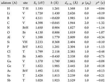
The electronic band structures of b-As and w-As phases near the fundamental band gap region and the total and orbital projected densities of states are shown inFigure 2. Notably, the total densities of states of these two phases display critical differences, which can be revealed by optical absorption and UV photoemission experiments. While states originated from p orbitals of As dominate the edges of valence and conduction bands, d orbitals appear in the conduction band. The carrier mobility at the top of the valence and at the bottom of the conduction bands of w-As near X-point is expected to be large. Adsorption of Adatoms. The adsorption of adatoms to b-As and w-b-As structures is analyzed by calculation of the equilibrium adsorption site, optimized atomic structure and energetics, which results in local electronic and magnetic states, charge transfer between adatom, and substrate. Our calculated results are presented inTable 1for the adatoms adsorbed to SL b-As substrate and inTable 2 for the adatoms adsorbed to SL w-As substrate. In the following sections we examine the details of the adsorption for each adatom.
Optimized Structure and Energetics of Adsorbed Ada-toms. At the optimized equilibrium site, all adatoms treated in this paper form chemical bonds with SL b-As and w-As substrates. Upon the chemisorption of these adatoms, local deformations even reconstructions in the 2D crystal structure of the substrate can occur. In the case of reconstruction, regular honeycomb or washboard structures are destroyed locally; host atom is pushed away from its position by substitution of adatoms like B and C.
First, we consider the adsorption of adatoms to the b-As substrate. The optimized atomic structures of adsorbed adatoms are shown in Figure 3, where local modifications in the atomic configurations around the adatom are described. The adatoms like H and Sb has binding energies≈ 1.0 eV. The binding energies of adatoms like Li, N, Al, Si, P, Cl, Ga, Ge, As, and Se are in the range of 1.5−2.5 eV. Some of these adatoms, like N, Si, P, and As, lead to local reconstruction. On the other hand, adatoms B, C, and O from thefirst row of the Periodic Table and Ti have binding energies ranging from 3.4 to 4.6 eV and give rise to strong local reconstructions. In particular, B and C adatoms substitute the lower lying As host atom by pushing
it down. It appears that the stronger the binding, the more severe the reconstruction. While host As atoms are three-fold-coordinated in arsenene phases, B and C adatoms become four-fold coordinated. Notably, adsorption of Ga does not cause any dramatic reconstruction leading to cluster formation in spite of the fact that Ga and As form tetrahedrally coordinated, 3D ionic compound GaAs. According to the Bader analysis,35Li, Al, Ge, and As donate charge to b-As substrate; the rest of the Table 1. Values Calculated by Using PBE for an Adatom (A) Adsorbed to Each (4× 4) Supercell of the SL b-As Substratea
adatom (A) site Eb(eV) h (Å) dA−As(Å) μ (μB) ρ* (e)
H T-H 1.185 1.261 1.568 1.0 −0.84 Li V 1.720 1.430 2.626 0.0 +0.19 B V 4.511 −0.620 1.985 1.0 −0.84 C V 4.398 −0.645 1.944 2.0 −1.32 N BrH 1.650 0.904 1.827 0.0 −1.14 O Br 4.130 0.806 1.819 0.0 −1.07 Al V 1.598 1.779 2.809 0.0 +0.34 Si VH 2.233 0.368 2.404 0.0 −0.10 P BrV 1.812 1.281 2.304 1.0 −1.13 Cl T 1.799 2.158 2.385 1.0 −0.48 Ti Br 3.405 −0.450 2.338 0.0 −0.75 Ga V 1.570 1.780 2.865 0.0 −0.08 Ge T 1.622 1.985 2.445 2.0 +0.18 As BrV 1.492 1.531 2.425 1.0 +0.13 Se T 2.428 1.813 2.239 0.0 −0.21 Sb T 1.028 1.923 2.529 1.0 −0.02
aAdsorption site A; the binding energy E
b; the height (distance) of the
adatom from the original, high-lying As atomic plane of the substrate h; the smallest distance between the adatom and As atom of the substrate dA−As; the local magnetic moment μ; the charge transfer
between the adatom and the substrateρ* with positive sign indicating the donation of electrons to the substrate.
Table 2. Values Calculated by Using PBE for an Adatom (A) Adsorbed to Each (3× 4) Supercell of the SL w-As Substratea
adatom (A) site Eb(eV) h (Å) dA−As(Å) μ (μB) ρ* (e)
H T 1.315 1.739 1.565 1.0 −0.79 Li T-H 2.021 1.519 2.587 0.0 +0.32 B T-H 4.575 −0.061 2.022 1.0 −0.81 C T-H 4.304 0.142 1.863 0.0 −0.83 N BrH 2.968 0.676 1.787 1.0 −1.43 O T-H 4.201 0.798 1.697 0.0 −1.40 Al T-H 2.226 1.726 2.597 0.0 +0.66 Si BrH 2.788 1.316 2.394 0.0 −0.02 P T-H 2.045 1.181 2.336 1.0 −0.49 Cl T 2.064 2.382 2.367 1.0 −0.41 Ti T-H 3.235 1.463 2.487 2.0 −0.72 Ga T-H 2.053 1.659 2.674 0.0 +0.41 Ge V 2.432 1.434 2.484 0.0 +0.07 As V 1.706 1.493 2.410 1.0 −0.06 Se T-H 2.341 1.641 2.266 0.0 −0.23 Sb V 1.376 1.731 2.573 1.0 +0.03
aAdsorption site A; the binding energy E
b; the height (distance) of the
adatom from the original, high-lying As atomic plane of the substrate h; the smallest distance between the adatom and the As atom of the substrate dA−As; the local magnetic moment μ; the charge transfer
between the adatom and the substrateρ* with positive sign indicating the donation of electrons to the substrate.
adatoms receive charge from the substrate. In Figure 4, the isosurfaces of the total charge density and the difference charge density Δρ are presented for Ti, Ge, and As adatoms, where bond formation, charge accumulation, and depletion regions are clearly seen.
Optimized atomic configurations of adatoms adsorbed to the w-As phase are shown inFigure 5. All adatoms except B and C are located above the upper atomic plane of w-As. B and C adatoms are implemented into the w-As layer. Due to changes in the optimized adsorption geometry, the binding energies and also the charge transfers between adatoms and substrate undergo changes. The atomic structure of w-As appears to be more robust under adsorption of adatoms; severe reconstruc-tions as in b-As do not take place except the cases of B and C. Accordingly, calculated binding energies of a majority of adatoms range between 1.4 and 2.4 eV. The rest of the adatoms, B, C, N, O, Si, and Ti, have relatively stronger binding in the energy range from 2.8 to 4.6 eV. As Li, Al, and Ga donate electrons to w-substrate, H, B, C, N, O, P, Cl, and Ti receive a significant amount of electronic charge from the substrate. These differences in the adsorption geometries of adatoms between b-As and w-As give rise to changes in the local electronic and magnetic properties, which will be discussed in forthcoming subsections.
Figure 3.Top and side views of the equilibrium (optimized) atomic structure of the adsorbed adatom and SL b-As phase. While host As atoms are shown by blue (dark) balls, adsorbed adatoms are indicated by balls of different colors and sizes.
Figure 4.TotalρT and difference Δρ charge density isosurfaces of
selected adatoms adsorbed to b-As. Isosurface value is 0.02 electrons/ Å3. Charge depletion and accumulation regions are indicated by
red-dark and gray-light isosurfaces.
In view the calculated atomic configurations and binding energies, one deduces the following trends in addition to those discussed above: The binding energies of Group V, Group IV, and Group III elements increase with increasing row number. Only N adatom on b-As becomes an exception. Also, light adatoms like Li, B, and C and Group III adatoms prefer to adsorb at the V-site. The distance between the adatom and the host As, dA−As, increases with increasing row number of the adatom.
Electronic and Magnetic Properties. The prime objective of doping of SL structures has been to modify their electronic and magnetic properties. Adsorbed adatoms can modify the electronic and magnetic structure of the b-As and w-As phases locally. In the doping at very low coverage, single adsorbed or substituted foreign atoms give rise to localized states in the fundamental band gap or resonance states in the band continua of the b-As and w-As phases.
The present analysis uses a scheme to deduce the effects of adsorption, in particular, energy shifts of adatom induced localized states relative to the“bare” extended substrate. To this end, rather than the energy bands of the supercells, here the total and adatom projected densities of states are examined to reveal the energy locations of dopant states relative to the fundamental band gap of the bare extended substrate as shown inFigures 6and7. The density of states of the bare extended substrate and the energy position of its fundamental band gap is retrieved from the local density of states LDOS (i.e., the
projected total density of states) calculated at As atom of the substrate, which is farthest from the adatom. This way, the energy positions of adatom-induced localized states can be determined relative to the band edges of the bare extended substrate with reasonable accuracy. The common Fermi level,36 which separates filled states from the empty states of the adatom + supercell system, is normally within the fundamental band gap; it can move toward the band edges depending on the character of the localized states. We note that because of the finite size of the supercell the coupling between farthest host As atom and a few specific adatoms can give rise to small uncertainties of in the exact position of band edges. Nevertheless, these uncertainties do not affect our discussion here. In Figures 6 and 7, the densities of states of the bare extended substrate and the fundamental band gap Egbetween its valence and conduction band edges are indicated. In what follows, we examine the features of calculated electronic and magnetic properties.
Important features of the electronic structure associated with the single adatom adsorbed to b-As are presented inFigure 6. States derived from hydrogen adatom adsorbed to b-As are spin polarized and appear near the edge of the valence band. Spin-up states occur below the Fermi level and hence become occupied. The spin-down states are located in the gap. Lithium adatom donates part of its valence charge to the states which overlaps with the bottom of the conduction band of the extended substrate. This situation implies that the adatom + Figure 5.Top and side views of the equilibrium (optimized) atomic structure of the adsorbed adatom and SL As phase. While As atoms of the w-As structure are shown by blue (dark) balls, adsorbed adatoms are indicated by balls of different colors and sizes.
substrate system is metallized at high coverage of Li. Spin-polarized unoccupied localized states induced by B are located near the valence and conduction band edges of the extended substrate. Carbon adatom displays a similar situation; while the spin-polarized, occupied localized state induced by C adatom is ∼0.2 eV above the valence band edge, the unoccupied one is ∼0.3 eV below the edge of the conduction band edge. This way the fundamental band gap is locally reduced by 0.5 eV. Nitrogen induces partially occupied, localized states in the band gap, empty localized states at the edge of conduction band, and resonance states in band continua.
Oxygen, which is strongly electronegative, has a high binding energy and receives a significant amount of electronic charge from the b-As substrate. Oxygen-induced states occurring below the valence band edge keep the fundamental band gap clean from localized states. Aluminum has an odd number of electrons and gives rise to occupied states at the valence band edge and donor states just below the conduction band edge. Similar to Al, Si has occupied states above the valence band edge and empty states just below the conduction band edge. Hence, the band gap is locally reduced to∼0.9 eV. While the occupied, localized spin-up states of P occur above the edge of the valence band, the empty spin-down state is localized at mid gap leaving only a 0.3 eV local band gap. In the case of Cl, a localized and occupied state at the midgap pins the Fermi level, whereas the next empty Cl localized state in the fundamental gap occurs∼0.3 eV above it. Titanium adatom, which leads to
significant local reconstruction, has occupied localized states above the edge of the valence band. Unoccupied Ti-derived
states in the fundamental gap occur ∼0.5 eV above the
occupied states. Gallium adatom having an odd number of valence electrons pins the Fermi level near the edge of the conduction band. Owing to the even number of valence electrons, the localized gap states derived from Ge arefilled, but empty localized states occur below the edge of the conduction band. Occupied spin-up states of As adatom pin the Fermi level near the edge of the valence band. Empty spin-down states occur at mid gap. All states derived from Se are located near the edge of the valence band and arefilled. Filled spin-up states and partially occupied spin-down states of Sb are located in the fundamental band gap. As seen, the adatoms add diversity of electronic features to b-As depending on their valence electrons and chemical interaction with the substrate.
The density of states related with the chemisorption of single adatoms adsorbed to the w-As substrate is illustrated inFigure 7. The bare extended substrate has a relatively small band gap, almost one-half of the band gap of bare b-As. The details of adsorption of adatoms can be seen in Table 2. Comparing
Figure 7 with Figure 6 corresponding to the adsorption of adatoms to b-As some trends are common, except that the splitting of adatom-derived occupied and unoccupied localized states in the fundamental band gap is smaller in w-As. Crucial differences associated with the magnetic state of adatoms are also recognized. For example, Ti (Ge) is spin polarized Figure 6.Calculated total densities (shown by thin light green lines) and adatom projected densities (shown by thin red-black lines) of states for a single-adatom adsorbed to each (4× 4) supercell of SL b-As substrate. The density of states of the bare extended b-As substrate shown in light blue is obtained from the local density of states calculated at a host As atom which is farthest from the adatom; its band gap is shown by the light blue zones. The zero of the energy is set at the common Fermi level shown by the dashed vertical line. For clarity, the projected densities of states of specific adatoms H and Li are shown by insets.
(unpolarized) on w-As, while it is spin unpolarized (polarized) on b-As. Additionally, curvatures of band edges of w-As differ from those of b-As, and hence, the Fermi level is prone to be affected from the finite size of the supercell. For example, the Fermi level can move out from the edges of the fundamental band gap. In what follows we discuss the adatom-induced features of the electronic structure.
The spin-up state of the adsorbed H adatom occurs near the edge of the valence band and is occupied. The empty spin-down state is near the midgap. A small, local gap of∼0.25 eV occurs between these localized states of H adatom. Adsorbed Li donates electrons to the states overlapping with the edge of the conduction band of w-As substrate. This situation causes the reduction of the photoelectric threshold of w-As substrate at high Li coverage. Boron-adsorbed b-As substrate is spin polarized with empty spin-down states at the midgap region. In contrast to b-As, states derived from the adsorbed C adatom are spin unpolarized; whilefilled states are below the edge of the valence band, empty states occur at the midgap. Similar to B, N-derived spin-up, localized states are below the edge of the valence band and spin-down, unoccupied states occur in the fundamental band gap. In the case of adsorbed O adatom, the fundamental band gap is clean from localized states; all O-derived states occur in the valence band. While the occupied states are derived from adsorbed Al at the edge of the conduction band, similar states of Si adatom are at midgap but empty ones are in the conduction band. Both occupied and empty spin-down states derived from P are in the fundamental
band gap and separated by a ∼0.4 eV local gap, whereas the occupied spin-up states occur near the edge of the valence band and attribute one-half metallic character to the system. A similar situation is found in the Ti-adsorbed w-As substrate having an integer number of Bohr magneton per supercell. Ga displays features similar to those of Al adatom. Thefilled states of Ge adatom at the midgap is separated from the empty states by a local gap of∼0.35 eV. Interestingly, Sb like other pnictogens N, P, and As gives rise to localized and occupied spin-up states and empty spin-down states, all having 1.0μBmagnetic moment per
supercell.
We note that the band energies of excited states of b-As and w-As, in particular, the fundamental band gap, are under-estimated by∼0.5 eV in calculations using PBE. For example, the PBE band gap of b-As is increased from 1.57 to 2.23 eV upon HSE correction.33Under these circumstances, the energy positions of unoccupied adatom derived states relative to the actual conduction band edge can be affected slightly. This effect can be even smaller if the same scissor operation of bare arsenene substrates is also applicable to the adatom + As substrate system. However, the energies of those states below the Fermi level corresponding to the ground state of adatom− substrate system and resulting charge exchange can be predicted by PBE calculations with reasonable accuracy.
Finally, we note that a recent study23 has treated the adsorption of B, C, and O to b-As using a similar method and predicted binding energies in fair agreement with the present paper, except C adatom, whose binding energy is less than one-Figure 7.Calculated total densities (shown by thin light green lines) and adatom projected densities (shown by red-black lines) of states for a single-adatom adsorbed to each (3× 4) supercell of SL w-As structure. The density of states of the bare extended w-As substrate shown in light blue is obtained from the local density of states calculated at a host As atom farthest from the adatom; its band gap is shown by the light blue zones. The zero of the energy is set at the common Fermi level shown by the dashed vertical line.
third of the value inTable 1. Also, we found that the magnetic ground state of the N + b-As system23is actually 54 meV less favorable relative to a nonmagnetic state.
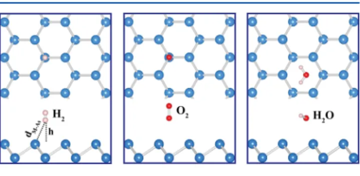
Physisorption of Molecules to SL Arsenene Phases. Three molecules, H2, O2, and H2O, interact weakly with b-As
and w-As substrates; they do not engage in notable chemical interaction. The physisorption of these three molecules is investigated by placing them in their different possible configurations above various sites of these substrates at large distances. Then the atomic positions of the whole system, namely, molecule and substrate atoms, are optimized to attain minimum total energy as well as atomic forces. The optimized structures corresponding to minimum total energy are presented inFigures 8and 9. Calculated values regarding the binding energies and molecule−substrate distances are listed in
Tables 3and4.
Weak vdW interaction between molecules and SL arsenene substrates reflects the optimized atomic configuration and corresponding energetics. The binding energy of H2is 69 and
81 meV on b-As and w-As, respectively, which is rather low and typical for vdW interaction. The situations for O2and H2O are
also similar to binding energies of 103 and 171 meV on b-As and 78 and 104 meV on w-As, respectively. As for the distances between molecules and As atom of the substrate, they are rather large in compliance with low binding energies.
Accordingly, SL arsenene phases are rather inert to H2, O2,
and H2O molecules, and hence, their dissociation of the
constituents is not expected in normal conditions. Also, the electronic properties of arsenene phases cannot be affected through the physisorption of these molecules.
Earlier, edges of flakes, vacancy defects, or specific adatoms adsorbed to SL graphene and MoS2were shown to be active
sites, where dissociations of molecules can be mediated.19,20 Notably, specific adatoms are expected to form relatively stronger bonds with some of these molecules. Here we examine edges of arsenene phases, which can either strongly bind or dissociate molecules. To this end we consider rectangular b-As and w-As flakes with different edge geometries as shown in
Figures 10and11.
In Figure 10one sees that H2, O2, and H2O molecules are
situated near the zigzag, armchair edges and their corners. Upon relaxation, H2O remains intact as a molecule, but near
the armchair edge H2 and O2 are dissociated spontaneously into their constituents saturating nearest, two-fold host As atoms. At the corner one of theflake, the dissociated O atoms change the 6-fold ring to a 5-fold by saturating host As. Similar processes are taking place at the edges of w-As as illustrated in
Figure 11. H2and O2molecules are dissociated spontaneously
at specific sites, and two constituent atoms are chemisorbed to the adjacent host atoms. Briefly, edges of the arsenene flakes form active sites to dissociate the constituents of H2 and O2
molecules. Earlier, it was found that while O2 molecule is
dissociated at the graphene vacancy, H2O remained intact.20
On the other hand, Mo atoms at the edges of vacancies in single-layer MoS2 were shown to mediate the dissociation of
H2O by forming strong Mo−H and S−OH bonds.
19 Apparently, since the binding of H2O is 5.63 and 3.93 eV
stronger than those of H2and O2molecules, respectively, the
reactivity of two-fold As atoms at the edges is not sufficient to dissociate H2O molecule.
■
CONCLUSIONSIn this paper we presented an extensive analysis of the chemical interaction between selected single adatoms and molecules with buckled b-As and symmetric washboard w-As phases of arsenene. Even if our analysis is focused on the single, isolated adatoms adsorbed and molecules physisorbed to single-layer arsenene, our results provide valuable information pertaining the functionalization and doping of arsenene in various applications.
Selected adatoms can form rather strong bonds with arsenene by exchanging electronic charges and cause local reconstructions. Also, the electronic states derived from these adatoms give rise to diversity of electronic structure with localized states in the fundamental band gap. Some of the adatoms acquire local magnetic moments through their spin-Figure 8.Top and side views of the atomic configurations of H2, O2,
and H2O molecules physisorbed to each (4× 4) supercell of b-As.
Figure 9.Top and side view of the atomic configurations of H2, O2,
and H2O molecules physisorbed to each (3× 4) supercell of w-As.
Table 3. Values Calculated by PBE for the Optimized Structure of the Single Molecule (M) Physisorbed to (4× 4) Supercell ofb-As Substratea
molecule (M) Ea(eV) h (Å) dM−As(Å)
H2 0.069 2.450 3.211
O2 0.103 2.630 3.367
H2O 0.171 2.615 3.275
aE
a, the physisorption energy of the molecule; h, the height of the
molecule from the original atomic plane of substrate; dM−As, the
minimum distance between the molecule and the substrate As atom.
Table 4. Values Calculated by PBE for the Optimized Structure of the Single Molecule (M) Physisorbed to (3× 4) Supercell of thew-As Phasea
molecule (M) Ea(eV) h (Å) dM−As(Å)
H2 0.081 2.185 3.024
O2 0.078 2.402 3.243
H2O 0.104 2.972 3.203
aE
a, the physisorption energy of the molecule; h, the height of the
molecule from the original atomic plane of substrate; dM−As, the
minimum distance between the molecule and the substrate As atom.
polarized electronic states even though arsenene phases are nonmagnetic semiconductors. Some adatoms can acquire half-metallic character at higher coverage.
Even though the interaction of molecules like H2, O2, and
H2O with nanomaterials is crucial for hydrogen storage, hydrogen evolution reaction, and oxidation−deoxidation processes, these molecules weakly interact with arsenene; their binding energies are very small and have predominantly vdW character. However, H2 and O2 can dissociate into its
constituent atoms at the edges of thefinite size flakes of b-As and w-As phases. The constituent atoms by themselves are chemisorbed to the low-coordinated As atoms and cause reconstruction at the edges.
■
AUTHOR INFORMATIONCorresponding Authors
*E-mail: [email protected]. Phone: +902562130835-1894. Fax: +902562135379.
*E-mail:[email protected]: +903122901216. Fax: +902562135379.
Notes
The authors declare no competingfinancial interest.
■
ACKNOWLEDGMENTSThe computational resources are provided by TUBITAK ULAKBIM, High Performance and Grid Computing Center (TR-Grid e-Infrastructure). E.A. and S.C. acknowledgefinancial support from the Academy of Sciences of Turkey (TÜBA). This study has been performed while E.A. was visiting the Department of Physics, Bilkent University.
■
REFERENCES(1) Özçelik, V. O.; Aktürk, O. Ü; Durgun, E.; Ciraci, S. Prediction of a Two-Dimensional Crystalline Structure of Nitrogen Atoms. Phys. Rev. B: Condens. Matter Mater. Phys. 2015, 92, 125420.
(2) Li, L.; Yu, Y.; Ye, G. J.; Ge, Q.; Ou, X.; Wu, H.; Feng, D.; Chen, X. H.; Zhang, Y. Black Phosphorus Field-Effect Transistors. Nat. Nanotechnol. 2014, 9, 372−377.
(3) Zhu, Z.; Tománek, D. Semiconducting Layered Blue Phosphorus: A Computational Study. Phys. Rev. Lett. 2014, 112, 176802.
(4) Kamal, C.; Ezawa, M. Arsenene: Two-Dimensional Buckled and Puckered Honeycomb Arsenic Systems. Phys. Rev. B: Condens. Matter Mater. Phys. 2015, 91, 085423.
(5) Aktürk, O. Ü; Özçelik, V. O.; Ciraci, S. Single-Layer Crystalline Phases of Antimony: Antimonenes. Phys. Rev. B: Condens. Matter Mater. Phys. 2015, 91, 235446.
(6) Zhang, S.; Yan, Z.; Li, Y.; Chen, Z.; Zeng, H. Atomically Thin Arsenene and Antimonene: Semimetal-Semiconductor and Indirect-Direct Band-Gap Transitions. Angew. Chem., Int. Ed. 2015, 54, 3112− 3115.
(7) Kohn, W.; Sham, L. J. Self-Consistent Equations Including Exchange and Correlation Effects. Phys. Rev. 1965, 140, A1133− A1138.
(8) Durgun, E.; Tongay, S.; Ciraci, S. Silicon and III-V Compound Nanotubes: Structural and Electronic Properties. Phys. Rev. B: Condens. Matter Mater. Phys. 2005, 72, 075420.
(9) Cahangirov, S.; Topsakal, M.; Aktürk, E.; Şahin, H.; Ciraci, S. Two- and One-Dimensional Honeycomb Structures of Silicon and Germanium. Phys. Rev. Lett. 2009, 102, 236804.
(10) Tsai, H. S.; Wang, S. W.; Hsiao, C. H.; Chen, C. W.; Ouyang, H.; Chueh, Y. L.; Kuo, H. C.; Liang, J. H. Direct Synthesis and Practical Bandgap Estimation of Multilayer Arsenene Nanoribbons. Chem. Mater. 2016, 28, 425−429.
Figure 10.Side and top views of atomic configurations of H2, O2, and H2O molecules interacting with the zigzag and armchair edges of b-Asflake.
While H2and O2dissociate at specific edges into constituent atoms, which, in turn, are adsorbed to host As atoms, H2O remains intact.
Figure 11.Side and top views of atomic configurations of H2, O2, and H2O molecules interacting with different edges of w-As flake. While H2and O2
dissociate at specific edges into constituent atoms, which, in turn, are adsorbed to host As atoms, H2O remains intact. The Journal of Physical Chemistry C
(11) Chan, K. T.; Neaton, J. B.; Cohen, M. L. First-Principles Study of Metal Adatom Adsorption on Graphene. Phys. Rev. B: Condens. Matter Mater. Phys. 2008, 77, 235430.
(12) Ataca, C.; Aktürk, E.; Ciraci, S.; Ustunel, H. High-Capacity Hydrogen Storage by Metallized Graphene. Appl. Phys. Lett. 2008, 93, 043123.
(13) Sevinçli, H.; Topsakal, M.; Durgun, E.; Ciraci, S. Electronic and Magnetic Properties of 3D Transition-Metal Atom Adsorbed Graphene and Graphene Nanoribbons. Phys. Rev. B: Condens. Matter Mater. Phys. 2008, 77, 195434.
(14) Durgun, E.; Ciraci, S.; Yildirim, T. Functionalization of Carbon-Based Nanostructures with Light Transition-Metal Atoms for Hydrogen Storage. Phys. Rev. B: Condens. Matter Mater. Phys. 2008, 77, 085405.
(15) Ersan, F.; Arslanalp, Ö.; Gökoğlu, G.; Aktürk, E. Effects of Silver Adatoms on the Electronic Structure of Silicene. Appl. Surf. Sci. 2014, 311, 9−13.
(16) Ding, Y.; Wang, Y. Structural, Electronic, and Magnetic Properties of Adatom Adsorptions on Black and Blue Phosphorene: A First-Principles Study. J. Phys. Chem. C 2015, 119, 10610−10622.
(17) Ersan, F.; Gökoğlu, G.; Aktürk, E. Adsorption and Diffusion of Lithium on Monolayer Transition Metal Dichalcogenides (MoS2(1−x)Sex) Alloys. J. Phys. Chem. C 2015, 119, 28648−28653.
(18) Aktürk, O. Ü; Aktürk, E.; Ciraci, S. Effects of Adatoms and Physisorbed Molecules on the Physical Properties of Antimonene. Phys. Rev. B: Condens. Matter Mater. Phys. 2016, 93, 035450.
(19) Ataca, C.; Ciraci, S. Dissociation of H2O at the Vacancies of
Single-Layer MoS2. Phys. Rev. B: Condens. Matter Mater. Phys. 2012,
85, 195410.
(20) Topsakal, M.; Şahin, H.; Ciraci, S. Graphene Coatings: An Efficient Protection from Oxidation. Phys. Rev. B: Condens. Matter Mater. Phys. 2012, 85, 155445.
(21) Topsakal, M.; Gürel, H. H.; Ciraci, S. Effects of Charging and Electric Field on Graphene Oxide. J. Phys. Chem. C 2013, 117, 5943− 5952.
(22) Gürel, H. H.; Ciraci, S. Enhanced Reduction of Graphene Oxide by Means of Charging and Electric Fields Applied to Hydroxyl Groups. J. Phys.: Condens. Matter 2013, 25, 435304.
(23) Li, Y.; Xia, C.; Wang, T.; Tan, X.; Zhao, X.; Wei, S. Light Adatoms Influences on Electronic Structures of the Two-Dimensional Arsenene Nanosheets. Solid State Commun. 2016, 230, 6−1.
(24) Li, Z.; Xu, W.; Yu, Y.; Du, H.; Zhen, K.; Wang, J.; Luo, L.; Qiu, H.; Yang, X. Monolayer Hexagonal Arsenene with Tunable Electronic Structures and Magnetic Properties via Impurity Doping. J. Mater. Chem. C 2016, 4, 362−370.
(25) Wang, Y. P.; Zhang, C. W.; Ji, W. X.; Wang, P. J. Unexpected Band Structure and Half-Metal in Non-Metal-Doped Arsenene Sheet. Appl. Phys. Express 2015, 8, 065202.
(26) Du, J.; Xia, C.; Wang, T.; Zhao, X.; Tan, X.; Wei, S. First-Principles Studies on Substitutional Doping by Group IV and VI Atoms in the Two-Dimensional Arsenene. Appl. Surf. Sci. 2016, 378, 350−356.
(27) Grimme, S. Semiempirical GGA-Type Density Functional Constructed with a Long-Range Dispersion Correction. J. Comput. Chem. 2006, 27, 1787−1799.
(28) Blöchl, P. E. Projector Augmented-Wave Method. Phys. Rev. B: Condens. Matter Mater. Phys. 1994, 50, 17953−17979.
(29) Perdew, J. P.; Burke, K.; Ernzerhof, M. Generalized Gradient Approximation Made Simple. Phys. Rev. Lett. 1996, 77, 3865−3868.
(30) Kresse, G.; Furthmüller, J. Efficient Iterative Schemes for Ab Initio Total-Energy Calculations Using a Plane-Wave Basis Set. Phys. Rev. B: Condens. Matter Mater. Phys. 1996, 54, 11169−11186.
(31) Monkhorst, H. J.; Pack, J. D. Special Points for Brillouin-Zone Integrations. Phys. Rev. B 1976, 13, 5188−5192.
(32) Heyd, J.; Scuseria, G. E.; Ernzerhof, M. Hybrid Functionals Based on a Screened Coulomb Potential. J. Chem. Phys. 2003, 118, 8207.
(33) Heyd, J.; Scuseria, G. E.; Ernzerhof, M. Hybrid Functionals Based on a Screened Coulomb Potential [J. Chem. Phys. 118, 8207 (2003)]. J. Chem. Phys. 2006, 124, 219906.
(34) Paier, J.; Marsman, M.; Hummer, K.; Kresse, G.; Gerber, I. C.; Ángyán, J. G. Erratum: Screened Hybrid Density Functionals Applied to Solids [J. Chem. Phys. 124, 154709 (2006)]. J. Chem. Phys. 2006, 125, 249901.
(35) Henkelman, G.; Arnaldsson, A.; Jónsson, H. A Fast and Robust Algorithm for Bader Decomposition of Charge Density. Comput. Mater. Sci. 2006, 36, 354−360.
(36) In our discussion, the Fermi level is the energy level, which separates the filled states from the empty states of the adatom +supercell system. Notably, for the systems containing very dilute adatoms or dopants Fermi level has to be determined through the chemical potential of the Fermi−Dirac distribution.