ThAA3
4:15pm-4:30pm .
25 Pair InAlAs / InAlGaAs DBR
InP Substrate
High-speed InGaAs Based Resonant
Enhanced p-i-n Photodiodes
25x None (121/112)
600 pm Semi Insulating
Ibrahim Kimukin, Necmi BiyiMi,
Ekmel
OzbayDepartment of Physics, Bilkent University, Ankara 06533, Turkey kimukinG;fsn.bilkent.edu.tr, Tel: +90 312 290 2305, Fax: +90 312 266 4579
Cavity
High-speed, high-efficiency photodetectors play an important role in optical communication and measurement systems. The photodiode performance is measured by the bandwidth-efficiency product (BWE) and is limited for conventional vertically illuminated photodiodes (VPDs) due to the bandwidth- efficiency tradeoff [ I]-[3]. This tradeoff arises from the fact that the quantum efficiency and bandwidth of a conventional VPD, have inverse dependencies on the photoabsorption layer thickness. To overcome the BWE limitation for such conventional VPDs, two alternative detection schemes were offered: edge-coupled photodiodes and resonant-cavity-enhanced photodiodes (RCE-PDs). Both PD structures have demonstrated excellent performances and are potential candidates as photodetectors for future high bitrate optical communication systems [4]-[8]. The ease of fabrication, integration, and optical coupling makes the RCE-PD more attractive for high-performance photodetection.
We used the transfer matrix method to design the epilayer structure and to simulate the optical properties of the photodiode. The details of the epitaxial structure we have used is given in Table 1. The bottom Bragg mirror is made of 25 pair quarter-wave stacks (InAIAs / Ino.aAlo.13Gao.34As) centered at 1550 nm. The structure was grown by solid-source MBE on semi insulating InP substrate. The reflectivity measurements showed that the thickness of the epilayers were 4% thicker than our design. This shifted the high reflectivity center of the bottom mirror to 1610 nm.
The samples were fabricated by a microwave-compatible process. First ohmic contact to n+ layer was formed by recess etch with a phosphoric acid based etchant that was followed by a self-aligned Au-Ge-Ni liftoff. The pf ohmic contact was achieved by Au/Ti lifioff. The samples were then rapid thermal annealed at 400 "C. Using .an isolation mask, we etched away all of the epilayers down to the undoped layer except the active areas. Then we
evaporated TilAu interconnect metal which formed the coplanar waveguide (CPW) transmission lines on -top of the semi-insulating substrate. The next step was the deposition of silicon nitride layer using PECVD. Finally, a 0.7 pm Au layer was evaporated as an airbridge to connect the center of the CPW to the p+ ohmic metal.
70 3 1
1450 1500 ,1550 1600 1650 1700
Wavelength (nm)
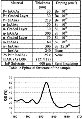
Figure 1: Spectral quantum efficiency (QE) measurement of the photodiode with resonance tuned to 1570 nm.
Photo response measurements were camed out in the 1450-1700 nm range, by using a tungsten-halogen projection lamp as the light source and a single pass monochromator. Output of the monochromator was coupled to a multimode fiber. The monochromatic light was
delivered to the devices by a lightwave fiber probe, and the electrical characterization was carried on a probe station. Large area diodes were chosen to ensure all the optical power was incident on the active area. We etched the top InGaAs and InAlAs layers in small steps and measured the quantum efficiency (QE) of the detectors. The peak efficiency at the resonance wavelength remained above 60% between 1570 and 1600 nm. Figure 1 shows the spectral QE of a photodetector whose resonance has been tuned to 1570 nm. We also measured similar quantum efficiencies from small area diodes (1 00 pm2) using a tunable laser.
We then measured the responses of the photodiodes under high incident optical powers. At the resonance wavelength of the detector, we changed the incident optical power and measured the resulting photocurrent. The photoresponse increases linearly with the input optical power up to 0.5 mW. The photoresponse deviated from linearity above 0.5 mW, and saturated near 1.2 mW. Figure 2 shows the measured photocurrent as a function of the optical power.
0.6 i
I I I t
0.0 0.2 0.4 0.6 0.8 1.0 1.2 Incident Power (mw)
Figure 2: Photocurrent versus incident optical power.
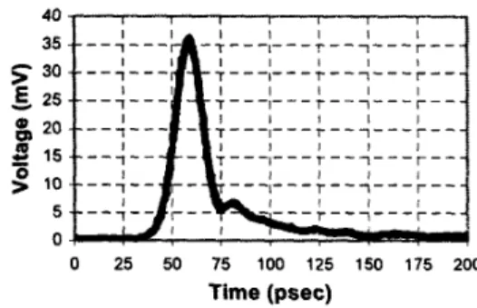
High-speed measurements were made with 1 ps FWHM optical pulses obtained from an erbium doped fiber laser operating at 1550 nm. Below 2 V reverse bias, the response of the diode had a long tail due to the diffusion of the holes. Above 2 V, the temporal response improved significantly. Figure 3 shows the temporal response of a small area photodiode
measured with 50 GHz sampling scope at 7 V biased with a 40 GHz bias-tee. Apart from a small tail, the shape of the response is a Gaussian with a 16 psec FWHM. When the 40
GHz limit due to the bias-tee was taking into account, the deconvolved fourier transform of the data had a 3-dB bandwidth of 3 1 GHz. The corresponding bandwidth efficiency product was 19 GHz for these diodes.
This work is supported by Turkish Department of Defense Grant No. KOBRA- 001, NATO Grant No. S P 9 7
Science Foundation Grant No. and Thales JP8.04. 4 0 ,
,
,,
970, National INT-9906220, 1 - - - r - - - - 1 - - - r - - 1 1 - -- -
0 25 50 75 100 125 150 175 200 Time (psec) Figure 3: Pulse response of a photodiode.References
[I] K. Kato, IEEE Trans.Microwave Theory Tech.,
(21 Y . G . Wey, et. al., J. Lightwave Technol., vol. 13, pp. 1490-1499, (1995).
[3] I. H. Tan, et. al., IEEE Photon. Technol.Lett.,
(41 G . S. Kinsley, et.al, IEEE Photonics Technology Letters, Vol. 12, pp. 416-418, (2000). [SI Jin-Wei Shi, et. al., IEEE Photonics Technology Letters, Vol. 13, pp. 623-625, (2001). [6] C. Lennox, et. al., IEEE Photon.Techno1. Lett.,
[7] E. Ozbay, et. al., Appl. Phys. Lett., vol. 74, no. [SI N. Biyikli, et. al., IEEE Photon. Technol. Lett., vol. 47, pp. 1265-1281, (1998). vol. 7, pp. 1477-1479, (1995). vol. 11,pp. 1162-1164,(1999). 8, pp. 1072-1074, (1999). vol. 13, pp. 705-707, (2001). 890