High performance multimaterial fibers and devices
Tam metin
Şekil

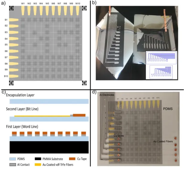
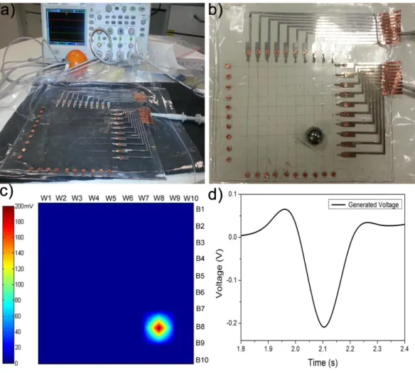
![Figure 10. Examples of pressure sensitive electronic skins, model hands and sensors. a) [62], b) [59], f) [68], g) [53].](https://thumb-eu.123doks.com/thumbv2/9libnet/5778556.117273/31.892.195.776.131.774/figure-examples-pressure-sensitive-electronic-skins-model-sensors.webp)


Benzer Belgeler
STATA istatistik programının kullanıldığı analiz sonucuna göre kişi başı ortalama ödeme istekliliği 84,69 TL olarak hesaplanmıştır.. Kişi başı ortalama
Araştırma sonucuna göre bir şekilde Sürdürülebilirlik Endeksi’nde yer alan yani BİST 50 ve Sürdürülebilirlik, Kurumsal Yönetim ve Sürdürülebilirlik Endeksleri ya
As shown in Figures 4 and 5, the audiovisual association had different effects on the subsequent perceived directions of regular and reverse-phi motions [three-way repeated-measures
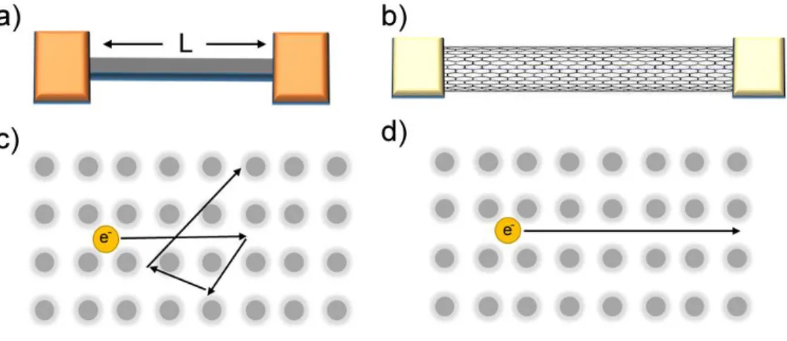
Highly-doped silicon has a very high attenuation coefficient (1.61µm −1 at plasma wavelength, λ = 9.42µm), therefore almost no power is transmitted through the structure beyond
The objectives of the present study were to: 1) evalu- ate, in vitro, the intracellular properties of MGd, spe- cific to atherosclerotic plaques, by confirming the inter- nalization
^ Variables are: 1) commercial bank debt; 2) concessional debt; 3) variable-rate debt; 4) short-term debt; 5) FDI; 6) public sector debt; 7) multilateral debt; 8) the ratio
Nüket Esen, “Ahmet Mithat: Hayat ve Külliyat” adlı makalesinde, yazarın kül- liyatı bir bütün olarak ele alındığında, şahsi macerasının ortaya döküldüğünü
In this approach, since there is no interaction between the MPLS and WDM layer control planes during the design phase, some lightpaths in the designed logical topology may not
